EP0062235A2 - Device for converting information from an electrical to an optical shape and vice versa - Google Patents
Device for converting information from an electrical to an optical shape and vice versa Download PDFInfo
- Publication number
- EP0062235A2 EP0062235A2 EP82102442A EP82102442A EP0062235A2 EP 0062235 A2 EP0062235 A2 EP 0062235A2 EP 82102442 A EP82102442 A EP 82102442A EP 82102442 A EP82102442 A EP 82102442A EP 0062235 A2 EP0062235 A2 EP 0062235A2
- Authority
- EP
- European Patent Office
- Prior art keywords
- optical
- information
- light
- modulator
- electrical
- Prior art date
- Legal status (The legal status is an assumption and is not a legal conclusion. Google has not performed a legal analysis and makes no representation as to the accuracy of the status listed.)
- Withdrawn
Links
Images


Classifications
-
- G—PHYSICS
- G02—OPTICS
- G02F—OPTICAL DEVICES OR ARRANGEMENTS FOR THE CONTROL OF LIGHT BY MODIFICATION OF THE OPTICAL PROPERTIES OF THE MEDIA OF THE ELEMENTS INVOLVED THEREIN; NON-LINEAR OPTICS; FREQUENCY-CHANGING OF LIGHT; OPTICAL LOGIC ELEMENTS; OPTICAL ANALOGUE/DIGITAL CONVERTERS
- G02F1/00—Devices or arrangements for the control of the intensity, colour, phase, polarisation or direction of light arriving from an independent light source, e.g. switching, gating or modulating; Non-linear optics
-
- G—PHYSICS
- G11—INFORMATION STORAGE
- G11C—STATIC STORES
- G11C11/00—Digital stores characterised by the use of particular electric or magnetic storage elements; Storage elements therefor
- G11C11/21—Digital stores characterised by the use of particular electric or magnetic storage elements; Storage elements therefor using electric elements
- G11C11/42—Digital stores characterised by the use of particular electric or magnetic storage elements; Storage elements therefor using electric elements using opto-electronic devices, i.e. light-emitting and photoelectric devices electrically- or optically- coupled or feedback-coupled
Definitions
- the invention relates to an arrangement for converting information from the electrical form into the optical form and / or vice versa according to the preamble of claim 1.
- xy matrices which are connected to IC circuits (integrated circuits) for addressing and multiplexing.
- IC circuits integrated circuits
- 1024 electrical connections between the IC circuits and the display are required.
- the invention has for its object to develop an arrangement of the type mentioned, with which it is possible to do without the large number of electrical connections in the aforementioned addressing of displays.
- the invention creates a new addressing technique in which only two connections are required for addressing.
- still images can be generated with liquid crystals without an inherent memory effect, and the display can also be used to digitize the movement of an optical pen, for example.
- the display can also be used for measurements, whereby the display works like a photodiode or CCD matrix.
- the most important elementary part of the invention is the electro-optically fed back memory elements which can be connected in series to shift registers.
- the shift register can be made up of photoresistor elements or photodiodes, which, for example, with thin film technology together with an electrical conductor arrangement on a substrate, e.g. a large glass plate.
- the optical modulators which give rise to the electro-optical feedback can, for example, be liquid crystals which lie between the substrate and a cover plate made of, for example, glass and which are coated on the inside with a light-polarizing layer and a transparent film.
- the shift register can be controlled electrically and / or optically.
- the information between the memory cells in the shift register is shifted in that two or more light-emitting or laser diodes with different emission wavelengths are switched on in a specific order, whereby one-phase, two-phase or three-phase optical control can be obtained.
- the invention relates to a new type of arrangement with which primarily optical displays can be modulated and optical digitizers can be scanned.
- electrical information can be fed serially or in parallel into a one- or two-dimensional optical modulator, which in display applications has the task of providing image information to the viewer.
- An optical pen can be used to transmit information from man to machine, which supplies the optical modulator with optical information which can be read electrically in serial or parallel form by electro-optical means.
- optical modulators which enter the electro-optical circuits as active elements, can also be used for light modulation in, for example, a display.
- FIG. 1 shows a basic electro-optical circuit with an optical modulator 2 and a photodetector 4.
- the optical modulator can be of different types. For example, it can be a liquid crystal, a Kerr cell, an electrically controlled Fabry-Perrot filter, an electrically controlled birefringent filter Franz-Keldysh modulator or an electrostatic light modulator.
- the function of the modulator 2 is to modulate the light from the light source 3 so that one can control with the voltage U in the power of the light reaching the photodetector.
- the photodetector 4, which is a photoresistor, lies in an electrical circuit consisting of the voltage source 5 and the fixed resistor 6. An output voltage U out can be tapped at the resistor 6.
- Resistor 1 describes the input resistance of modulator 2. If modulator 2 is a liquid crystal, for example, a high input resistance for the circuit is obtained, and at the same time the output resistance can be chosen to be relatively low. A transmission characteristic (voltage amplification, current amplification, impedance conversion, etc.) is obtained between the input and the output of the electro-optical circuit according to FIG. 1, which can be compared with a field effect transistor. In principle, this makes it possible to build amplifiers, active electronic filters, oscillators, non-linear elements, switches, logic circuits, delay elements, flip-flops, shift registers, memories, etc. with the aid of EG circuits (electro-optical circles) according to FIG. 1. The invention relates in particular to arrangements for electro-optical shift registers and memories which can be used for addressing and / or modulating light in one- or two-dimensional modulators and for scanning and / or reading in digitizers.
- FIG. 2 shows a circle with a photodiode which is important for the invention.
- the input stage is the same as in FIG. 1, but in this case the output stage consists of a photo diode 7, whereby the voltage source can be dispensed with.
- the circuit according to FIG. 2 works like a voltage / current converter, in which the degree of amplification can be controlled by the light intensity of the light source 3.
- FIG. 3a the input part of the circuit from FIG. 1 is simply connected to the output of the circuit.
- FIG. 3b the same applies to FIG. 3b, but with the difference that the voltage across the resistor forms the output. If an increased voltage on the optical modulator 2 causes less light attenuation and thus more illumination of the photoresistor 4, thereby reducing its resistance, positive feedback is obtained in FIG. 3a and negative feedback in FIG. 3b.
- a further photo resistor 4b is provided in the circuits according to FIGS. 3c and 3d, which is provided with a further optical modulator 2b. Because the modulators are cross-connected, stronger nonlinear relationships can be generated, which, however, is not necessary according to FIG. 4b.
- FIG. 4c shows an example of a bridge circuit with photodiodes
- FIG. 4d shows the possibility of connecting photodiodes in series in order to increase the modulation voltage for modulator 2.
- 7, 7a to 7d are photodiodes
- 8, 9, 9a to 9b are fixed resistors
- 2, 2a to 2b are optical modulators and 3a to 3b are light sources.
- FIGS. 3 and 4 Various types of memory elements and flip-flops can be constructed with the aid of the electro-optical feedback according to FIGS. 3 and 4.
- Figure 5a shows a simple memory element with a photo resistor. With the help of the switch 10 the element is activated and with the help of the switches 11 or 12 the element is set to zero. It is assumed that the light source 3 lights up because the switch 12 is closed and the voltage source 13 is thus connected to the light source 3. If both switches 10 and 11 are open, there is no voltage across resistor 6 and if the electro-optical modulator has a characteristic as shown in FIG. 5c, which can be achieved, for example, with liquid crystals, we are in point A of the transmission curve in FIG. 5c. When the switch 11 is closed, the voltage U.
- FIG. 5b shows a corresponding memory element which works with a photodiode instead of with a photo resistor.
- a sufficiently high voltage is applied via the switch 15 placed on the modulator 2 so that its operating point reaches the ascending branch of the characteristic curve (to the right of C in FIG. 5c).
- the storage element is thereby placed in the logical position 1 (position D in FIG. 5 c) and held in this position by the voltage of the photodiode 7.
- the memory element is set to the logical position 0, in that the operating point of the modulator 2 changes to the position B in FIG. 5c.
- the storage properties of the elements in FIG. 5 are obtained from two stable states of the electro-optical feedback, which were caused by a non-linearity in the transmission curve of the optical modulator.
- An alternative feedback option for obtaining a memory property is the cross circuit shown in FIG. 6, the circuit in FIG. 6a working with photo resistors and that in FIG. 6b working with photo diodes.
- FIG. 6b shows an electro-optical SR flip-flop with photodiodes.
- optical modulators 20a and 20b with negated characteristics are used here, which means that an increase in the voltage at the modulator causes a reduction in light transmission.
- switch 12 When switch 12 is closed, switch 19 is closed for a shorter or longer period of time; the voltage at modulator 20a is low, the light transmission through modulator 20a is high, the voltage at photodiode 7a is high, the voltage across modulator 20b is high, the light transmission through modulator 20b is low, the voltage at photodiode 7b is low, etc. It can thus be defined that the photodiode 7a is set to one and the photodiode 7b is set to zero. If, instead, the switch 18 is closed, the SR flip flip flip flips so that the photodiode 7a is set to zero and the photodiode 7b is set to one.
- a shift register is obtained by cascading the SR flip-flops, which is shown in FIG. 7 with photoresistor circuits.
- the first SR multivibrator operates in the manner described with reference to FIG. 6a. It is assumed that the switch 19 has set the photoresistor 4a1 to one and thus the photoresistor 4b1 to zero. If the switch 21 is now closed for a moment, the light transmission through the modulator 2c1 increases and the resistance of the photoresistors 17a1 and 17b1 decreases during the time the switch is closed.
- both flip-flop 1 (4a1) and flip-flop 2 (4a2) are set to one.
- the flip-flop 1 can be set to zero by closing the switch 18 is posed.
- the switch 24 can then be closed for a moment, as a result of which the logic one stored in the flip-flop 2 is transferred to the flip-flop 3, which is therefore set to one.
- the flip-flops can be isolated from one another in pairs during the information transmission, whereby the risk of information degradation is considerably less than if the isolating stages were connected to one and the same switch.
- the flip-flops in Figure 7 are controlled by two-phase control pulses. Of course, apart from a single-phase or two-phase control, a three-phase control can also be carried out.
- a shift register according to FIGS. 8, 9 and 10a is obtained when using a one, two or three-phase control. If, in FIG. 8a, the light source 3 illuminates the optical modulators 2a, 2b, etc., the switch 11 is closed and the switch 10 is closed for a brief moment, the optical modulator 2a has - as can be seen from the explanations for FIG. 5a a large light transmission, and the photo resistors 4a and 23a have small resistance values.
- the switch 21 If the switch 21 is then closed for a short time interval corresponding to the time constant of the optical modulators, a pulse reaches the modulator 2b which is large enough to set the memory element b to one. By repeated actuations of the switch 21 ones ' in the shooting incrementally shifted register to the right. In order to shift zeros, an interaction between the switches 21 and 11 is necessary in such a way that first switch 21 is closed, then switch 11 is opened, then switch 11 is closed and then switch 21 is opened. As a result, the switch 21 sets all elements to the right of an element set to one to one, while the switch 11 sets all other elements to zero.
- FIG. 8b shows a shift register with two-phase control, in which the information is transferred between the memory elements with the aid of the electro-optical isolating stages described with reference to FIG. If the element to the left of a separation stage is set to one, when the switches 21a or 21b are closed, the element to the right is set to one, and if the element to the left is set to zero, the element to the right is set to zero .
- the isolators are made up of optical modulators (2a1, 2b1, etc.) connected to switches 21a and 21b, and photo-resistors (17a, 17b, 17c, etc.) placed between the connection points of resistors 6 and 14 of two adjacent elements are connected.
- FIG. 9 shows a shift register with two-phase control, which corresponds to the embodiment according to FIG. 8a.
- a switch 24 has been added to the circuit in FIG. 8a.
- the photoresistor 23 for information transmission between the elements is connected to the switch 21 for every second element and to the switch 24 for the other elements. As a result, the information transmission takes place within isolated pairs, which is related to the control pulse time (the time during which the switches 21 and 24 are closed) puts.
- a three-phase control according to FIG. 10a can be used.
- the memory elements are constructed and connected to one another in the same way as those in FIG. 8a, but the photo resistors have a different supply here.
- the photo resistors 23a and 4a are connected to the switch 25, the photo resistors 23b and 4b to the switch 26, the photo resistors 23c and 4c to the switch 27 and the photo resistors 23d and 4d to the switch 25, etc. every third memory element receives the same control pulse.
- the following control pulse sequence is required: 25 is closed, 10 is closed, 10 is opened (a is set to one), 26 is closed (b is set to one), 25 is opened (b is from a isolated), 27 is closed (c is set to one), 26 is opened (c is isolated from b), 25 is closed (a is set to zero, d is set to one) etc.
- the whole shift register can be opened Be zeroed that all switches 25 to 27 are opened simultaneously or that the light source is extinguished for a moment.
- FIG. 12 An alternative to the use of electrical switches 21, 24, 25, 26, 27, 30, etc. for controlling the electro optical shift register is an optical controller illustrated by Figures 12 and 13.
- the electrical switches can be replaced by photo resistors which are actuated by light, which is shown in FIG. 12 for the two-phase control (see FIG. 9).
- Figure 12 has a simpler electrical wiring system, but a more complex optical system.
- the switches 10, 12a and 12b are operated in the following switching sequence (it is assumed that the light source 3a through the optical filter 43 and the optical filters 40a, b, c etc. modulators 2a, b, c etc.
- 11 is closed, 10 is closed for a moment (a is set to one), 12b is closed for a moment (b is set to one via 23a and 37a).
- 23a is illuminated by light source 3a via 43, 40a and 2a, and 37a is illuminated by 3c via 41 and 38a when 12b is switched on, 12a is closed for a moment (c is set to one via 23b and 37b, where 37b illuminated by 3b) etc.
- the optical filters 38a, b, c, etc. only let light that has passed through the filter 41, the filters 39a, b, c, etc. only let light from the filter 42 through, and the filters 40a, b, c, etc. Allowing only light from filter 43 to pass through can optically address photoresistors 37a, b, c, these photoresistors not being affected by light from light source 3a.
- FIG. 14 shows how the memory element b in FIG. 13a can be implemented if the optical modulators are a liquid crystal.
- FIG. 14b shows the element in section along the section line AA in FIG. 14a.
- a Substrate 67 is coated with a reflective layer 66, photoresist material 4b, light-polarizing insulator material 65, electrically conductive layers 50, 51, resistance material 6b, a transparent electrically conductive layer 53 and an interference filter layer 45a.
- the liquid crystal 64 is applied between the base substrate 67 and a transparent pane 61, which is covered on the underside with a transparent, electrically conductive layer 62 and a light-polarizing layer 63.
- the direction of polarization of the liquid crystal 64 relative to the direction of polarization of the polarizing layers 63 and 65 is chosen such that the voltage 0 between the layers 62 and 53 causes a certain light transmission, while a somewhat higher voltage at the layer 53 causes a lower transmission. If, however, the voltage across layer 53 is increased above a certain value, the transmission increases again.
- the lowest transmission can be due to the fact that the direction of polarization of the light that passes through the crystal 64 and the direction of polarization of the insulating material 65 differ by 90 °.
- the fine adjustment of the position of the operating points on the transmission curve according to FIG. 5c can be done by applying a suitable pretension to the layer 62.
- the individual electrical components in the memory element b in FIG. 13a can easily be identified on the basis of FIG. 14a and to some extent on the basis of FIG. 14b.
- the electrical supply occurs through the conductive strips 50 and 51, which are connected at points 55, 56 and 57 to the resistors 23b, 4b and 6b, respectively.
- the electrical contact of these connections comes about because there is no insulating layer 65.
- the same technique is used to exclude 4b and 6b from the liquid crystal electrode in points 52 and 53b to the electrode of the next memory element in points 58, corresponding to point 59 in the memory element b, to connect.
- FIG. 15 shows an example for the production of a memory element which is constructed using photodiodes according to FIG. 13b.
- the photodiodes consist of a p-layer 77 and an n-layer 78.
- the photodiode 7b is connected at 70 to the electrode 69 and at 71 to the conductor 73.
- the photodiode 33b is at point 75 to the electrode of the next storage element and at point 74 to the conductor 73 through an electrically conductive arm 72.
- FIG. 15b which is a section along the line AA in FIG. 15a represents.
- the base substrate 67 is provided with a reflecting layer 66, n-conducting semiconductor material 78, p-conducting semiconductor material 77, light-polarizing insulating material 65, a transparent electrical conductor 69, an interference filter 45a, a liquid crystal 64, a light-polarizing layer 63, and a transparent electrical conductor 62 and a transparent pane 61.
- the element is illuminated from the top side. If the substrate 67 is semiconductor material, the photodiode element can be manufactured according to known technology.
- FIGS. 16 and 17 show two-dimensional displays with memory elements according to FIG. 13a and FIG. 14.
- the memory element 60a can be set to one when inputting information, and with the switches 12a, b and c, the information in the shift register with the memory cells 60a, b, c, d and e can be white be pushed.
- ⁇ 1 , ⁇ 2 and ⁇ 3 define the center wavelengths for the interference filters in the memory elements and in front of the light sources.
- the memory cells 60a-60e pass on information to the horizontal shift registers which represent the display.
- the information transfer from the vertical shift register to the horizontal shift registers takes place via the photoresistors 80a-80d, which are provided with the interference filters 79a-79d with the central wavelengths ⁇ 4 and ⁇ 5 , alternately every second with ⁇ 4 and ⁇ 5 . Since the filters 81 and 82 in front of the light sources 3d and 3e have the central wavelengths ⁇ 4 and ⁇ 5 , the switches 12d and 12e can be used to control the information in the display.
- the photo resistors 80 (FIG. 16b) are connected between the points 58 (FIG. 14a) of the elements in the vertical shift register and the point 59 of the respective first element in the horizontal shift registers.
- ⁇ 1 , 1 2 and for the three main colors are selected, a certain color rendering can be achieved by suitable selection of the switching sequence.
- the size of the storage elements can be adapted to the information density such that a large display element is followed by two small storage elements before the next large display element in the shift register follows. If both plates 61 and 67 in FIG. 14b are transparent, the display can be made transparent, as a result of which the light sources 3a-3e are arranged behind the display when viewed by the viewer.
- the shift register 60a-60e in Figure 16 can be viewed as a y address register.
- FIG. 17 shows how xy addressing can be carried out by providing the plate 67 (FIG. 14b) with a shift register 6a-f, which is connected to the horizontal electrodes 81a-e, and the plate 61 with another shift register 60g - 601 provides that is connected to the vertical electrodes 81g - k. If the two plates 61 and 67, the liquid crystal forms an optical modulator for both the memory elements 60a-1 and for the display, which is controlled by the voltage between the transparent electrodes 81a-e and 81g-k.
- the shift register 61a-f is controlled by light sources arranged in a panel on the top of the plates 61, 67 and the shift register 60g-1 is controlled by light sources arranged under the plates 61, 67.
- the photo resistors 80a-k serve to read the voltage state of the memory elements of the shift registers between the control cycles.
- the resistors 82a-k and 80a-k are selected so that the liquid crystal, for example when the memory elements 60d and 60h are set to one, assumes a transmission state deviating from the environment at the cross point between 81d and 81h. If the liquid crystal has a usable stereoscopic effect, the circuit according to FIG. 17 can be used to program still images into the display using suitable switching sequences for the light sources 10a, b. If the liquid crystal does not have a memory effect, the usual scanning technique can be used.
- FIG. 18 shows how the shift register in FIG. 13a can be supplemented for reversible operation.
- FIG. 13a only one photo resistor 83 has been added per storage element. With this resistor, the information can be pushed back to the previous storage element by controlling the light sources in reverse order.
- FIG. 20 shows a shift register which, in addition to the input of electrical information in a series representation by means of the switch 10, can also be used for the parallel input of optical information, which is an electrical series representation for the amplifier 88 and the electronics unit 89, which are, for example, a computer can be directed.
- the shift register is a modification of the shift register shown in FIG. 10a, but a corresponding modification can also be carried out for the other shift registers described.
- the modification is that the memory elements are provided with a third photoresistor 87, which can set the memory element to one when the switch 85 is closed and light in the range of wavelength ⁇ 1 which is passed through the filter 86 illuminates the photoresistor .
- the light for illuminating the modulators 2a, b, c etc. in the shift register is selected so that it does not contain any wavelengths in the range around ⁇ 1 .
- a light wavelength ⁇ 2 can be used to reset (erase) a memory element. (see the storage element d with the additional fetus resistor 108).
- FIG. 21 shows how a memory element can be realized in FIG. 21.
- 61 is an upper transparent plate
- 62 a transparent, electrically conductive layer
- 63 a light-polarizing layer
- 64 a liquid crystal
- 53 a transparent electrically conductive layer
- 51, 90, 91, 92 and 93 electrically conductive strips
- 65 an insulating layer
- 4c a photoresist layer
- 6c a resistance layer and 67 a base plate.
- Figure 21a shows the memory element from above.
- the strips 90, 91 and 92 are the control pulse lines which are controlled by the switches 27, 26 and 25, respectively (cf. FIG. 20).
- 93 is the line for controlling the writing of the optical information.
- the photoresistor 4c is connected at point 94 to the strip 90 and at point 52 to the electrode 53 and the resistance element 6c, which is connected at its other end to the conductor 51 common to all memory elements at point 57.
- the photoresistor 23c is connected at one end via the point 94 to the strip 90 and the supply line to the resistor 4c and at the other end to the electrode of the next memory element at point 58.
- the electrode 53 is connected at point 96 to the photoresistor 87c, which is connected at its other end to the strip 93 at point 95.
- 87c is covered with an interference filter 86c, which filters out the light that is used for the electro-optical feedback of the memory element.
- a combined display and digitizer can be constructed with the aid of memory elements of the type shown in FIGS. 20 and 22, which is shown in FIG.
- a long shift register is obtained which is electrically controlled by switches 25 to 27 and into which electrical information (ones and zeros) can be fed with the aid of switch 10.
- the information After passing through the shift register (97a, b, c, etc.), the information can be output again using the amplifier 88.
- the function of the storage elements is ensured by the light from the light source 3a, which passes through the filter 98, the task of which is to light in the area around the Filter out wavelength ⁇ 1 .
- the light from the light source 3b passes through the filter 99, which filters out the light in the range around the wavelength ⁇ 1 , and is used for the optical input of information into the memory element.
- the optically entered information is output via the amplifier 88 with the help of the switches 25-27.
- optical information can be entered using an optical pen.
- electro-optical memory elements, flip-flops and shift registers dealt with in this description can be combined in a large number of ways in order to obtain displays and digitizers with different properties.
Landscapes
- Physics & Mathematics (AREA)
- Engineering & Computer Science (AREA)
- Computer Hardware Design (AREA)
- Nonlinear Science (AREA)
- General Physics & Mathematics (AREA)
- Optics & Photonics (AREA)
- Liquid Crystal (AREA)
- Optical Modulation, Optical Deflection, Nonlinear Optics, Optical Demodulation, Optical Logic Elements (AREA)
- Optical Communication System (AREA)
- Liquid Crystal Display Device Control (AREA)
Abstract
Die Erfindung betrifft eine Anordnung zur Umwandlung von Informationen aus der elektrischen Form in die optische Form (und umgekehrt), wobei die optische Informationsform eine in einer, zwei oder drei Richtungen zeitlich variierende Lichtintensität ist und wobei die Umwandlung der Information aus der elektrischen in die optische Form durch optische Modulatoren, z. B. Flüssigkristalle, erfolgt und die Umwandlung aus der optischen Form in die elektrische Form durch Fotodetektoren erfolgt. Die optischen Modulatoren und die Fotodetektoren werden zeitlich von einem oder mehreren elektrooptisch rückgekoppelten Kreisen gesteuert oder abgetastet, in denen sich mindestens ein optischer Modulator 2 im Strahlengang zwischen mindestens einer Lichtquelle 3, z. B. einer Leuchtdiode oder Laserdiode, und mindestens einem Fotodetektor 4, z. B. einem Fotowiderstand oder einer Fotodiode, befindet. Der Fotodetektor 4 ist in mindestens einen elektrischen Kreis 4, 5, 6 eingeschaltet, an welchen der optische Modulator 2 derart angeschlossen ist, daß man über einen Rückkopplungskreis, dessen Verhalten - in Kreisrichtung gesehen - bestimmt wird durch die Lichttransmission des optischen Modulators 2, die elektrische Eigenschaft des Fotodetektors und das elektrische Eingangssignal des optischen Modulators 2, eine positive und negative Rückkopplung erhält. Die elektrooptisch rückgekoppelten Kreise können auch mehr als einen optischen Modulator und Fotodetektor enthalten, aus denen eine elektrooptisch rückgekoppelte Kreuzschaltung aufgebaut wird.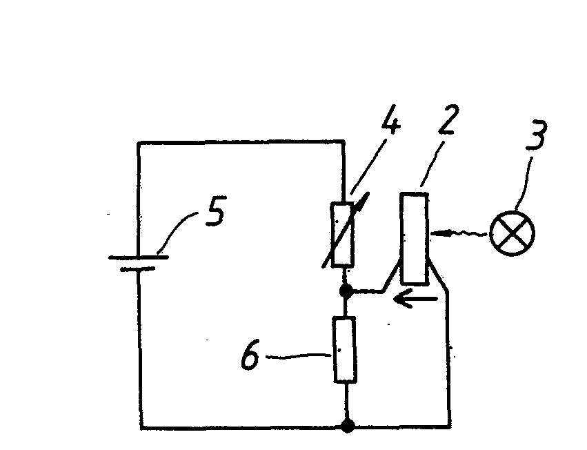
Description
Die Erfindung betrifft eine Anordnung zur Umwandlung von Informationen aus der elektrischen Form in die optische Form und/oder umgekehrt gemäß dem Oberbegriff des Anspruches 1.The invention relates to an arrangement for converting information from the electrical form into the optical form and / or vice versa according to the preamble of
Zur Adressierung von flachen Displays werden z.Zt. im wesentlichen xy-Matrizen benutzt, die an IC-Schaltkreise (integrierte Schaltkreise) zur Adressierung und Multiplexierung angeschlossen werden. Bei beispielsweise 512 x 512 Bildelementen sind dabei 1024 elektrische Verbindungen zwischen den IC-Schaltkreisen und dem Display erforderlich.For addressing flat displays, currently essentially used xy matrices, which are connected to IC circuits (integrated circuits) for addressing and multiplexing. For example, with 512 x 512 picture elements, 1024 electrical connections between the IC circuits and the display are required.
Der Erfindung liegt die Aufgabe zugrunde, eine Anordnung der eingangs genannten Art zu entwickeln, mit der es möglich ist, bei der vorstehend beispielsweise genannten Adressierung von Displays ohne die große Zahl von elektrischen Verbindungen auszukommen.The invention has for its object to develop an arrangement of the type mentioned, with which it is possible to do without the large number of electrical connections in the aforementioned addressing of displays.
Zur Lösung dieser Aufgabe wird eine Anordnung nach dem Oberbegriff des Anspruches 1 vorgeschlagen, die erfindungsgemäß die im kennzeichnenden Teil des Anspruches 1 genannten Merkmale hat.To solve this problem, an arrangement according to the preamble of
Vorteilhafte Weiterentwicklungen der Erfindung sind in den Unteransprüchen genannt.Advantageous further developments of the invention are mentioned in the subclaims.
Hinsichtlich der eingangs genannten Adressierung von Displays wird durch die Erfindung eine neue Adressiertechnik geschaffen, bei der nur zwei Verbindungen für die Adressierung notwendig sind. Außerdem können stillstehende Bilder mit Flüssigkristallen ohne innewohnenden Speichereffekt erzeugt werden, und das Display kann auch zur Digitalisierung der Bewegung beispielsweise eines optischen Schreibstiftes verwendet werden. Das Display kann auch für Messungen verwendet werden, wobei das Display wie eine Fotodiode oder CCD-Matrize arbeitet.With regard to the addressing of displays mentioned at the outset, the invention creates a new addressing technique in which only two connections are required for addressing. In addition, still images can be generated with liquid crystals without an inherent memory effect, and the display can also be used to digitize the movement of an optical pen, for example. The display can also be used for measurements, whereby the display works like a photodiode or CCD matrix.
Wichtigster elementarer Teil der Erfindung sind die elektrooptisch rückgekoppelten Speicherelemente, die zu Schieberegistern in Reihe geschaltet werden können. Das Schieberegister kann aus Fotowiderstandselementen oder Fotodioden.aufgebaut sein, die mit beispielsweise Dünnfilmtechnologie zusammen mit einer elektrischen Leiteranordnung auf einem Substrat, z.B. einer großen Glasplatte, integriert werden. Bei den optischen Modulatoren, die Anlaß zu der elektrooptischen Rückkopplung geben, kann es sich beispielsweise um Flüssigkristalle handeln, die zwischen das Substrat und einer Deckscheibe aus beispielsweise Glas liegen, die auf der Innenseite mit einer lichtpolarisierenden Schicht und einem transparenten Film belegt sind. Das Schieberegister kann elektrisch und/oder optisch gesteuert werden. Im letztgenannten Fall wird die Information zwischen den Speicherzellen im Schieberegister dadurch verschoben, daß zwei oder mehrere Leucht- oder Laserdioden mit verschiedenen Emissionswellenlängen in einer bestimmten Reihenfolge eingeschaltet werden, wodurch man eine einphasige, zweiphasige oder dreiphasige optische Steuerung erhalten kann.The most important elementary part of the invention is the electro-optically fed back memory elements which can be connected in series to shift registers. The shift register can be made up of photoresistor elements or photodiodes, which, for example, with thin film technology together with an electrical conductor arrangement on a substrate, e.g. a large glass plate. The optical modulators which give rise to the electro-optical feedback can, for example, be liquid crystals which lie between the substrate and a cover plate made of, for example, glass and which are coated on the inside with a light-polarizing layer and a transparent film. The shift register can be controlled electrically and / or optically. In the latter case, the information between the memory cells in the shift register is shifted in that two or more light-emitting or laser diodes with different emission wavelengths are switched on in a specific order, whereby one-phase, two-phase or three-phase optical control can be obtained.
Die Erfindung betrifft eine neue Anordnungsart, mit der in erster Linie optische Displays moduliert und optische Digitizer abgetastet werden können. Mit den in der Erfindung beschriebenen Anordnungen können elektrische Informationen seriell oder parallel in einen ein- oder zweidimensionalen optischen Modulator eingespeist werden, der bei Displayanwendungen die Aufgabe hat, Bildinformation an den Betrachter zu geben. Zur Informationsübertragung vom Menschen zur Maschine kann ein optischer Schreibstift verwendet werden, der dem optischen Modulator optische Informationen zuführt, die auf elektrooptischem Wege elektrisch in serieller oder paralleler Form abgelesen werden können.The invention relates to a new type of arrangement with which primarily optical displays can be modulated and optical digitizers can be scanned. With the arrangements described in the invention, electrical information can be fed serially or in parallel into a one- or two-dimensional optical modulator, which in display applications has the task of providing image information to the viewer. An optical pen can be used to transmit information from man to machine, which supplies the optical modulator with optical information which can be read electrically in serial or parallel form by electro-optical means.
Die Anordnungen, welche die Erfindung umfaßt, basieren auf elektrooptischen Kreisen,die in verschiedener Weise mit optischen Modulatoren integriert werden können. In einigen Fällen können auch die optischen Modulatoren, die als aktive Elemente in die elektrooptischen Kreise eingehen, zur Lichtmodulation in beispielsweise einem-Display verwendet werden.The arrangements which the invention encompasses are based on electro-optical circuits which can be integrated in various ways with optical modulators. In some cases, the optical modulators, which enter the electro-optical circuits as active elements, can also be used for light modulation in, for example, a display.
Zum näheren Verständnis soll die Erfindung anhand von Ausführungsbeispielen erläutert werden. Es zeigen
- Figur 1 - 8 elektrooptische Grundelemente gemäß der Erfindung, die durch verschiedene Kombinationen zum Aufbau der für die Erfindung wichtigen elektrooptischen Kreise verwendet werden können,
- Figur 9 - 23 Beispiele solcher aus den Grundelementen aufgebauten elektrooptischen Kreise.
- FIGS. 1-8 basic electro-optical elements according to the invention, which can be used by various combinations to build up the electro-optical circles important for the invention,
- Figures 9-23 examples of such electro-optical circles constructed from the basic elements.
Figur 1 zeigt eine elektrooptische Grundschaltung mit einem optischen Modulator 2 und einem Fotodetektor 4. Der optische Modulator kann unterschiedlicher Art sein. Beispielsweise kann es sich handeln um einen Flüssigkristall, eine Kerr-Zelle, ein elektrisch gesteuertes Fabry-Perrot-Filter, ein elektrisch gesteuertes doppelbrechendes Filter, ein Franz-Keldysh-Modulator oder einen elektrostatischen Lichtmodulator. Die Funktion des Modulators 2 besteht darin, das Licht von der Lichtquelle 3 so zu modulieren, daß man mit der Spannung Uin die Leistung des Lichtes steuern kann, das den Fotodetektor 4 erreicht. Der Fotodetektor 4, der ein Fotowiderstand ist, liegt in einem elektrischen Kreis, der aus der Spannungsquelle 5 und dem festen Widerstand 6 besteht. Am Widerstand 6 kann eine Ausgangsspannung Uout abgegriffen werden. Der Widerstand 1 beschreibt den Eingangswiderstand des Modulators 2. Wenn der Modulator 2 beispielsweise ein Flüssigkristall ist, so erhält man einen hohen Eingangswiderstand für den Kreis, und gleichzeitig kann der Ausgangswiderstand verhältnismäßig niederohmig gewählt werden. Zwischen dem Eingang und dem Ausgang des elektrooptischen Kreises gemäß Figur 1 erhält man eine übertragungscharakteristik (Spannungsverstärkung, Stromverstärkung, Impedanzumwandlung usw.), die mit einem Feldeffekttransistor verglichen werden kann. Hierdurch wird es im Prinzip möglich, mit Hilfe von EG-Kreisen elektrooptischen Kreisen)nach Figur 1 Verstärker, aktive elektronische Filter, Oszillatoren, nichtlineare Glieder, Schalter, logische Schaltkreise, Verzögerungselemente, Kippstufen, Schieberegister, Speicher usw. aufzubauen. Die Erfindung bezieht sich insbesondere auf Anordnungen für elektrooptische Schieberegister und Speicher, die zur Adressierung und/oder Modulation von Licht in ein- oder zweidimensionalen Modulatoren und zur Abtastung und/oder Auslesung in Digitizern verwendet werden können.FIG. 1 shows a basic electro-optical circuit with an
Durch Verwendung anderer Arten von Fotodetektoren als Fotowiderstände (Fotoleiter), wie z.B. Fotodioden, Fototransistoren, Fotozellen, Fotomultiplikatoren, Foto-Feldeffekttransistoren oder Fotokapazitäten kann eine andere übertragungscharakteristik erreicht werden. Einen für die Erfindung wichtigen Kreis mit einer Fotodiode zeigt Figur 2. Die Eingangsstufe ist die gleiche wie in Figur 1, doch hesteht die Ausgangsstufe in diesem Fall aus einer Fotodiode 7, wodurch auf die Spannungsquelle verzichtet werden kann. Im Prinzip arbeitet der Kreis nach Figur 2 wie ein Spannungs-/Strom-Wandler, bei dem der Verstärkungsgrad durch die Lichtintensität der Lichtquelle 3 gesteuert werden kann.By using other types of photo detectors than photo resistors (photo conductors), such as photo diodes, photo transistors, photo cells, photo multipliers, photo field effect transistors or photo capacities, a different transmission characteristic can be achieved. FIG. 2 shows a circle with a photodiode which is important for the invention. The input stage is the same as in FIG. 1, but in this case the output stage consists of a
Für die Schieberegister und Speicher, welche die Erfindung behandelt, ist die Möglichkeit, mit den elektrooptischen Kreisen gemäß Figur 1 und 2 elektrooptische Rückkopplungen vornehmen zu können, von entscheidender Bedeutung. Figur 3 zeigt sechs verschiedene Beispiele für elektrooptische Rückkopplung mit Fotowiderständen, während Figur 4 vier verschiedene Beispiele für elektrooptische Rückkopplung mit Fotodioden zeigt.For the shift registers and memories which the invention deals with, the possibility of being able to carry out electro-optical feedbacks with the electro-optical circuits according to FIGS. 1 and 2 is of crucial importance. Figure 3 shows six different examples of electro-optical feedback with photo resistors, while Figure 4 shows four different examples of electro-optical feedback with photo diodes.
In Figur 3a ist der Eingangsteil des Kreises aus Figur 1 einfach an den Ausgang des Kreises geschaltet. Für Figur 3b gilt das Gleiche, jedoch mit dem Unterschied, daß die Spannung am Widerstand den Ausgang bildet. Wenn eine erhöhte Spannung am optischen Modulator 2 eine geringere Lichtdämpfung und somit eine stärkere Beleuchtung des Fotowiderstandes 4 bewirkt, wodurch dessen Widerstand verkleinert wird, so erhält man in Figur 3a eine positive Rückkopplung und in Figur 3b eine negative Rückkopplung. In den Schaltungen nach Figur 3c und 3d ist ein weiterer Fotowiderstand 4b vorhanden, der mit einem weiteren optischen Modulator 2b versehen ist. Dadurch, daß die Modulatoren kreuzgeschaltet sind, kann man stärkere nichtlineare Zusammenhänge erzeugen, was jedoch gemäß Figur 4b nicht erforderlich ist. Negative Rückkopplungen kann man durch Umpolung des Modulators 2 erzielen. Figur 4c zeigt ein Beispiel einer Brückenschaltung mit Fotodioden, und Figur 4d zeigt die Möglichkeit, Fotodioden in Reihe zu schalten, um die Modulationsspannung für den Modulator 2 zu erhöhen. 7, 7a bis 7d sind Fotodioden, 8, 9, 9a bis 9b sind feste Widerstände, 2, 2a bis 2b sind optische Modulatoren und 3, 3a bis 3b sind Lichtquellen.In FIG. 3a, the input part of the circuit from FIG. 1 is simply connected to the output of the circuit. The same applies to FIG. 3b, but with the difference that the voltage across the resistor forms the output. If an increased voltage on the
Mit Hilfe der elektrooptischen Rückkopplungen gemäß Figur 3 und 4 können verschiedene Arten von Speicherelementen und Kippstufen aufgebaut werden. Figur 5a zeigt ein einfaches Speicherelement mit einem Fotowiderstand. Mit Hilfe des Schalters 10 wird das Element aktiviert, und mit Hilfe der Schalter 11 oder 12 wird das Element auf Null gestellt. Es wird angenommen, daß die Lichtquelle 3 deshalb leuchtet, weil der Schalter 12 geschlossen und die Spannungsquelle 13 somit an der Lichtquelle 3 liegt. Wenn beide Schalter 10 und 11 offen sind, ist am Widerstand 6 keine Spannung vorhanden und wenn der elektrooptische Modulator eine Charakteristik gemäß Figur 5c hat, was z.B. mit Flüssigkristallen erreichbar ist, befinden wir uns im Punkt A der Transmissionskurve in Figur 5c. Wenn der Schalter 11 geschlossen wird, steigt die Spannung U. am Widerstand 6 an, wodurch gemäß Figur 5c die Lichttransmission durch den Modulator 2 verringert wird, und folglich der Widerstandswert des Fotowiderstandes 4 erhöht und Uin verringert wird, was eine negative Rückkopplung bedeutet, die dem Modulator einen Transmissionwert gibt, welche dem Punkt B der Kurve in Figur 5c entspricht. Dieser Lage wird eine logische Null zugeordnet. Wenn der Schalter 11 nun für einen kurzen Augenblick geschlossen wird, so daß die Spannung am Modulator 2 den Wert Utrigg zu überschreiten gezwungen wird, dann än- dert sich die Rückkopplung von einer negativen in eine positive, und die Spannung Uinsteigt schnell auf ihren oberen Höchstwert U max Dieser Lage wird eine logische Eins zugeordnet. Wird dann der Schalter 11 oder 12 für einen kurzen Augenblick geöffnet, so rutscht der Arbeitspunkt auf der Transmissionskurve schnell wieder in die Lage B, in der er so lange liegen bleibt, bis der Schalter 10 wieder kurzfristig geschlossen wird. Die Schaltung nach Figur 5a stellt also ein logisches Speicherelement dar.Various types of memory elements and flip-flops can be constructed with the aid of the electro-optical feedback according to FIGS. 3 and 4. Figure 5a shows a simple memory element with a photo resistor. With the help of the
Figur 5b zeigt ein entsprechendes Speicherelement, das statt mit einem Fotowiderstand mit einer Fotodiode arbeitet. über den Schalter 15 wird eine ausreichend hohe Spannung an den Modulator 2 gelegt, damit dessen Arbeitspunkt auf den ansteigenden Ast der Kennlinie (rechts von C in Figur 5c) gelangt. Das Speicherelement wird dadurch in die logische Lage 1 gestellt (Lage D in Figur 5c) und in dieser Lage durch die Spannung der Fotodiode 7 gehalten. Durch kurzes Öffnen des Schalters 12 wird das Speicherelement in die logische Lage 0.gestellt, indem der Arbeitspunkt des Modulators 2 in die Lage B in Figur 5c übergeht.FIG. 5b shows a corresponding memory element which works with a photodiode instead of with a photo resistor. A sufficiently high voltage is applied via the
Die Speichereigenschaften der Elemente in Figur 5 erhält man durch zwei stabile Zustände der elektrooptischen Rückkopplungen, die durch eine Nichtlinearität in der Transmissionskurve des optischen Modulators verursacht wurden. Eine alternative Rückkopplungsmöglichkeit zur Gewinnung einer Speichereigenschaft ist die in Figur 6 gezeigte Kreuzschaltung, wobei die Schaltung in Figur 6a mit Fotowiderständen und-die in Figur 6b mit Fotodioden arbeitet.The storage properties of the elements in FIG. 5 are obtained from two stable states of the electro-optical feedback, which were caused by a non-linearity in the transmission curve of the optical modulator. An alternative feedback option for obtaining a memory property is the cross circuit shown in FIG. 6, the circuit in FIG. 6a working with photo resistors and that in FIG. 6b working with photo diodes.
Wenn in Figur 6a die Schalter 12 und 19 geschlossen sind und der Schalter 18 offen ist, hat der Modulator 2b eine hohe Lichttransmission, der Fotowiderstand 4b einen niedrigen Widerstandswert, der Modulator 2a eine niedrige Spannung und geringe Transmission und der Fotowiderstand 4a einen hohen Widerstandswert. Wenn der Schalter 19 geöffnet wird, gibt der hohe Widerstand des Fotowiderstandes 4a eine beibehaltene hohe Spannung über dem Modulator 2b, und der Modulator 2b behält seine hohe Transmission und der Modulator 2a seine niedrige Transmission. Dieser Zustand kann so definiert werden, daß der Fotowiderstand 4b auf Null und der Fotowiderstand 4a auf Eins gestellt ist. Wenn nun der Schalter 18 kurz geschlossen wird, so wird der Fotowiderstand 4b auf Eins und der Fotowiderstand 4a auf Null gestellt. Man erhält somit eine elektrooptische SR-Kippstufe. Die Stabilität der Kippstufe in ihren beiden Lagen hängt von der gegenseitigen Anpassung (Matching) der Komponenten 2a, 4a und 2b, 4b (Verstärkungsfaktor, Nullpunktswert) sowie von der Nichtlinearität dieser Komponenten ab.In Figure 6a, when the
Figur 6b zeigt eine elektrooptische SR-Kippstufe mit Fotodioden. Um negative elektrooptische Rückkopplungen zu erhalten, werden hier optische Modulatoren 20a und 20b mit negierter Charakteristik verwendet, was bedeutet, daß eine Erhöhung der Spannung am Modulator eine Senkung der Lichttransmission bewirkt. Ist der Schalter 12 geschlossen, und wird der Schalter 19 während einer kürzeren oder längeren Zeitspanne geschlossen; so ist die Spannung am Modulator 20a niedrig, die Lichttransmission durch den Modulator 20a groß, die Spannung an der Fotodiode 7a groß, die Spannung über dem Modulator 20b groß, die Lichttransmission durch den Modulator 20b niedrig, die Spannung an der Fotodiode 7b niedrig usw. Man kann also definieren, daß die Fotodiode 7a auf Eins und die Fotodiode 7b auf Null gestellt ist. Wenn stattdessen der Schalter 18-geschlossen wird, schlägt die SR-Kippstufe um, so daß die Fotodiode 7a auf Null und die Fotodiode 7b auf Eins gestellt wird.FIG. 6b shows an electro-optical SR flip-flop with photodiodes. In order to obtain negative electro-optical feedback,
Durch Kaskadenschaltung der SR-Kippstufen erhält man ein Schieberegister, welches in Figur 7 mit Fotowiderstandsschaltungen dargestellt ist. Wenn sämtliche optischen Modulatoren beleuchtet und die Schalter 21 und 24 offen sind, so arbeitet die erste SR-Kippstufe in der Weise, wie es anhand von Figur 6a beschrieben wurde. Es wird angenommen, daß der Schalter 19 den Fotowiderstand 4a1 auf Eins und damit den Fotowiderstand 4b1 auf Null gestellt hat. Wenn nun der Schalter 21 für einen Augenblick geschlossen wird, wird während der Zeit, während welcher der Schalter geschlossen ist, die Lichttransmission durch den Modulator 2c1 größer und der Widerstand der Fotowiderstände 17a1 und 17b1 kleiner. Hierdurch sinkt, die Spannung am Fotowiderstand 4b2, da dieser Fotowiderstand zu den Fotowiderständen 17a1 und 4d1 parallelgeschaltet ist, welche durch die unter Spannung gesetzten Modulatoren 2c1 bzw. 2b1 beleuchtet werden. Somit ist sowohl die Kippstufe 1 (4a1) als auch die Kippstufe 2 (4a2) auf Eins gestellt. In der nächsten Phase kann durch Schließen des Schalters 18 die Kippstufe 1 auf Null gestellt wird. Danach kann der Schalter 24 für einen Augenblick geschlossen werden, wodurch die in der Kippstufe 2 gespeicherte logische Eins auf die Kippstufe 3 übertragen wird, die also auf Eins gestellt wird. Wenn dann der Schalter 21 wieder für einen kurzen Augenblick geschlossen wird, wird die Null von der Kippstufe 1 auf die Kippstufe 3 übertragen, und die ursprüngliche logische Eins ist also um drei Stufen nach rechts verschoben worden-. Durch Verwendung von Trennstufen 17a1, 17b1, 2c1, 17a3, 17b3, 2c3 usw., die von dem Schalter 21 betätigt werden, und Trennstufen 17a2, 17b2, 2c2, 17a4, 17b4, 2c4 usw., die von dem Schalter 24 betätigt werden, können die Kippstufen bei der Informationsübertragung paarweise voneinander isoliert werden, wodurch die Gefahr einer Informationsdegradation erheblich geringer wird, als wenn die Trennstufen an ein und denselben Schalter angeschlossen wären. Man kann sagen, daß die Kippstufen in Figur 7 von zweiphasigen Steuerimpulsen gesteuert werden. Natürlich kann außer einer einphasigen oder zweiphasigen Steuerung auch eine dreiphasige Steuerung vorgenommen werden.A shift register is obtained by cascading the SR flip-flops, which is shown in FIG. 7 with photoresistor circuits. When all the optical modulators are illuminated and the
Wenn das Schieberegister aus Speicherelementen nach Figur 5a statt aus Kippstufen nach Figur 6a aufgebaut wird, so erhält man ein Schieberegister gemäß den Figuren 8, 9 und 10a bei Anwendung einer ein-, zwei- oder dreiphasigen Steuerung. Wenn in Figur 8a die Lichtquelle 3 die optischen Modulatoren 2a, 2b usw. beleuchtet, der Schalter 11 geschlossen ist und der Schalter 10 für einen kurzen Augenblick geschlossen wird, so hat - wie sich aus den Erläuterungen zu Figur 5a ergibt - der optische Modulator 2a eine große Lichttransmission, und die Fotowiderstände 4a und 23a haben kleine Widerstandswerte. Wenn dann der Schalter 21 für ein kurzes der Zeitkonstante der optischen Modulatoren entsprechendes Zeitintervall geschlossen wird., so gelangt ein Impuls an den Modulator 2b, der groß genug ist, das Speicherelement b auf Eins zu stellen. Durch wiederholte Betätigungen des Schalters 21 werden Einsen 'im Schieberegister schrittweise nach rechts verschoben. Um Nullen zu verschieben, ist ein Zusammenspiel zwischen den Schaltern 21 und 11 in der Weise erforderlich, daß zuerst Schalter 21 geschlossen wird, worauf Schalter 11 geöffnet, dann Schalter 11 geschlossen und dann Schalter 21 geöffnet wird. Dadurch stellt der.Schalter 21 alle Elemente, die rechts von einem auf Eins gestellten Element liegen, auf Eins, während der Schalter 11 alle übrigen Elemente auf Null stellt.If the shift register is built up from memory elements according to FIG. 5a instead of from flip-flops according to FIG. 6a, a shift register according to FIGS. 8, 9 and 10a is obtained when using a one, two or three-phase control. If, in FIG. 8a, the
Figur 8b zeigt ein Schieberegister mit zweiphasiger Steuerung, bei welchem die Informationsübertragung zwischen den Speicherelementen mit Hilfe der anhand von Figur 7 beschriebenen elektrooptischen Trennstufen geschieht. Wenn das links von einer Trennstufe liegende Element auf Eins gestellt ist, so wird beim Schließen der Schalter 21a oder 21b das rechts liegende Element auf Eins gestellt, und wenn das links liegende Element auf Null gestellt ist, so wird das rechts liegende Element auf Null gestellt. Die Trennstufen sind aus optischen Modulatoren (2a1, 2b1 usw.), die an die Schalter 21a und 21b angeschlossen sind, sowie aus Fotowiderständen (17a, 17b, 17c usw.) aufgebaut, die zwischen den Verbindungspunkten der Widerstände 6 und 14 zweier benachbarter Elemente angeschlossen sind. Die Schalter 21a und 21b werden abwechselnd geschlossen (zweiphasige Steuerung), damit bei der Informationsübertragung zwischen den Speicherelementen diese paarweise isoliert werden. Figur 9 zeigt ein Schieberegister mit zweiphasiger Steuerung, das der Ausführung gemäß Figur 8a entspricht. Gegenüber der Schaltung in Figur 8a ist ein Schalter 24 hinzugekommen. Der Fotowiderstand 23 zur Informationsübertragung zwischen den Elementen ist für jedes zweite Element an den Schalter 21 angeschlossen und für die übrigen Elemente an den Schalter 24. Hierdurch erfolgt die Informationsübertragung innerhalb isolierter Paare, was die an die Steuerimpulszeit (die Zeit, während welcher die Schalter 21 und 24 geschlossen sind) gestellten Ansprüche herabsetzt.FIG. 8b shows a shift register with two-phase control, in which the information is transferred between the memory elements with the aid of the electro-optical isolating stages described with reference to FIG. If the element to the left of a separation stage is set to one, when the
Um das Verschieben von Nullen nach dem in Figur 8a gezeigten Prinzip zu erleichtern, kann eine dreiphasige Steuerung gemäß Figur 10a angewendet werden. Die Speicherelemente sind in gleicher Weise wie die in Figur 8a aufgebaut und miteinander verbunden, doch haben die Fotowider< stände hier eine andere Speisung. Die Fotowiderstände 23a und 4a sind an den Schalter 25, die Fotowiderstände 23b und 4b an den Schalter 26, die Fotowiderstände 23c und 4c an den Schalter 27 und die Fotowiderstände 23d und 4d an den Schalter 25 angeschlossen usw., d.h. jedes dritte Speicherelement erhält denselben Steuerimpuls. Um eine Eins nach rechts zu verschieben, ist folgende Steuerimpulsfolge erforderlich: 25 wird geschlossen, 10 wird geschlossen, 10 wird geöffnet (a ist auf Eins gestellt), 26 wird geschlossen (b ist auf Eins gestellt), 25 wird geöffnet (b ist von a isoliert), 27 wird geschlossen (c ist auf Eins gestellt), 26 wird geöffnet (c ist von b isoliert), 25 wird geschlossen (a ist auf Null gestellt, d ist auf Eins gestellt) usw. Das ganze Schieberegister kann dadurch auf Null.gestellt werden, daß sämtliche Schalter 25 bis 27 gleichzeitig geöffnet werden oder daß die Lichtquelle für einen Augenblick gelöscht wird.In order to facilitate the shifting of zeros according to the principle shown in FIG. 8a, a three-phase control according to FIG. 10a can be used. The memory elements are constructed and connected to one another in the same way as those in FIG. 8a, but the photo resistors have a different supply here. The
Das Schieberegister kann auch aus Speicherelementen auf Fotodiodenbasis (Figur 5b) aufgebaut werden, wie dies Figur 10b zeigt. Die Speicherelemente können über die Steuerschalter 30 bis 32 und die Dioden 34a, b, c usw. auf Null gestellt werden, und die Informationsübertragung zwischen den Speicherelementen werden von den Fotodioden 33a, b, c usw. vorgenommen. Die Spannungsquelle 28 dient dazu, mit dem Schalter 29 das Speicherelement a bei der Informationseingabe auf Eins zu stellen. Die Schaltfolge für die Schalter 29 bis 32 beim Verschieben einer Eins durch das Register ist wie folgt:
- 31
und 32 werden geschlossen (b und c sind auf Null gestellt), 30 wird offen gehalten, 29 wird geschlossen, 29 wird geöffnet (a ist auf Eins gestellt), 31 wird geöffnet (b wirdvon 33a auf Eins gestellt), 30 wird geschlossen (a wird auf Null gestellt), 32 wird geöffnet (c wird auf Eins gestellt), 31 wird geschlossen (b wird auf Null gestellt) usw. Die bisher beschriebenen Schieberegister sind für digitale Informationen und können abwechselnd Einsen und Nullen verschieben, welche zwei verschiedenenLichttransmissionswerte der optischen Modulatoren entsprechen. Es besteht jedoch auch die Möglichkeit, analoge Information zu verschieben, was inFigur 11 veranschaulicht wird. Die analoge Information wird anden Kondensatoren 35a, b, c usw. aufgebaut, die einen gewissen Entladungswiderstand 36a, b, c usw. haben. Die folgende Schaltfolge kann verwendet werden: - 10 wird geschlossen, 25 wird geschlossen (35a wird auf die Spannung V. aufgeladen), 26 wird geschlossen (35b wird auf die Spannung Vin aufgeladen), 25 wird geöffnet, 27 wird geschlossen (35c erhält die Spannung Vin), 26 wird geöffnet, 10 wird geschlossen, 25 wird geschlossen, (35d erhält V. , 35a erhält einen neuen Wert für Vin) usw. Die Kondensatoren 35 werden über die
Fotowiderstände 4 aufgeladen, und wenn die Spannung anden Modulatoren 2 Null beträgt, hat die Transmission einen solchen Wert, daß der Stromüber den Fotowiderstand 4a denüber den Widerstand 36a fließenden Entladestrom ausgleicht. Wenn Vin größer als die Spannung am Kondensator ist, ist die Lichttransmission größer als der vorher genannte Wert, und der Kondensator 35 wird aufgeladen. Wenn Vin kleiner ist, wird der Kondensator überden Widerstand 36 entladen. Um die Degradation bei der Informationsübertragung zwischen den Speicherelementen zu verringern, können Trennstufen vorgesehen werden (siehe Figur 8b).
- 31 and 32 are closed (b and c are set to zero), 30 is kept open, 29 is closed, 29 is opened (a is set to one), 31 is opened (b is set from 33a to one), 30 becomes closed (a is set to zero), 32 is opened (c is set to one), 31 is closed (b is set to zero) etc. The shift registers described so far are for digital information and can alternately shift ones and zeros, which two correspond to different light transmission values of the optical modulators. However, there is also the possibility of shifting analog information, which is illustrated in FIG. 11. The analog information is built up on the
capacitors 35a, b, c etc., which have acertain discharge resistance 36a, b, c etc. The following switching sequence can be used: - 10 is closed, 25 is closed (35a is charged to voltage V.), 26 is closed (35b is charged to voltage V in ), 25 is opened, 27 is closed (35c receives voltage V in ), 26 is opened, 10 is closed, 25 is closed, (35d receives V., 35a receives a new value for V in ) etc. The capacitors 35 are charged via the
photoresistors 4, and if the voltage across themodulators 2 is zero, the Transmission is such a value that the current through thephotoresistor 4a compensates for the discharge current flowing through theresistor 36a. If V in is greater than the voltage across the capacitor, the light transmission is greater than the aforementioned value and the capacitor 35 is charged. If V in is less, the capacitor is discharged throughresistor 36. Separation stages can be provided in order to reduce the degradation in the information transmission between the storage elements (see FIG. 8b).
Eine Alternative gegenüber der Anwendung elektrischer Schalter 21, 24, 25, 26, 27, 30 usw. zur Steuerung der elektrooptischen Schieberegister ist eine optische Steuerung, die durch die Figuren 12 und 13 veranschaulicht wird. In dem einfachsten Fall können die elektrischen Schalter durch Fotowiderstände ersetzt werden, die durch Licht betätigt werden, was in Figur 12 für die zweiphasige Steuerung gezeigt ist (siehe Figur 9). Verglichen mit Figur 9 hat Figur 12 ein einfacheres elektrisches Leitungssystem, jedoch ein komplexeres optisches System. Bei der Verschiebung einer logischen Eins werden die Schalter 10, 12a und 12b in folgender Schaltfolge betätigt (es wird vorausgesetzt, daß die Lichtquelle 3a durch das optische Filter 43 und die optischen Filtern 40a, b, c usw. die Modulatoren 2a, b, c usw. kontinuierlich bestrahlt): 11 wird geschlossen, 10 wird für einen Augenblick geschlossen (a wird auf Eins gestellt), 12b wird für einen Augenblick geschlossen (b wird über 23a und 37a auf Eins gestellt). 23a wird von der Lichtquelle 3a über 43, 40a und 2a beleuchtet, und 37a wird von 3c über 41 und 38a beleuchtet, wenn 12b eingeschaltet ist), 12a wird für einen Augenblick geschlossen (c wird über 23b und 37b auf Eins gestellt, wobei 37b von 3b beleuchtet wird) usw.An alternative to the use of
Dadurch, daß die optischen Filter 38a, b,c usw. nur Licht durchlassen, das den Filter 41 passiert hat, die Filter 39a, b, c usw. nur Licht vom Filter 42 hindurchlassen und die Filter 40a, b, c, usw. nur Licht vom Filter 43 hindurchlassen, kann man die Fotowiderstände 37a, b, c optisch adressieren, wobei diese Fotowiderstände nicht durch Licht von der Lichtquelle 3a beeinflußt werden.Because the
Wenn man von der Speicherelementschaltung in Figur 10a ausgeht, kann man ein dreiphasiges optisch gesteuertes Schieberegister gemäß Figur 13a erhalten. Die Verschiebung einer Eins geschieht hier auf folgende Weise:
- 12c wird geschlossen, 10 wird für einen Augenblick geschlossen (das Speicherelemeht a wird auf Eins gestellt, indem
Spannungsquelle 5über 10 die Spannung an 6a erhöht und '3c über geöffneten 4a und 23a beleuchtet), 12b wird geschlossen (b wird auf Eins gestellt, daModulator 2a gleichzeitig3b über 2b 4b beleuchtet), 12c wird geöffnet (a wird auf Null gestellt), 12a wird geschlossen (c wird auf Eins gestellt, da3a über 46a und 2cwenn 10 geschlossen ist, andernfalls eine Null) usw.
- 12c is closed, 10 is closed for a moment (the memory element a is set to one by
Voltage source 5 over 10 increases the voltage at 6a and '3c over 47, 44a and themodulator 2a opened from '10 simultaneously illuminates 4a and 23a), 12b is closed (b is set to one, since 3b over 48, 45a and2b 4b illuminated), 12c is opened (a is set to zero), 12a is closed (c is set to one, since 3a is illuminated via 49, 46a and2c 4c), 12b is opened (b is set to zero), 12c is closed (d is set to one and at the same time a one is entered in a if 10 is closed, otherwise a zero) etc.
Optische Steuerung kann vorzugsweise auch für Speicherelemente mit Fotodioden (Figur 5b) verwendet werden, was in Figur 13b gezeigt ist. Eine Eins wird auf die folgende Weise verschoben:
- 12c wird geschlossen und 29 wird für einen Augenblick geschlossen (a wird dadurch auf Eins gestellt,
daß Schalter 29 das Element a aktiviert, und 3cüber die Komponenten 44a und 2a einen Fotostrom durch 7a erzeugt,der 2a auch dann geöffnet hält,wenn 29 nicht mehr geschlossen ist), 12b wird geschlossen (b wirdvom Fotostrom von 33a auf Eins gestellt undvon 7b, dievon 3b über45a und 2b beleuchtet wird, auf Eins gehalten), 12c wird geöffnet (a wird auf Null gestellt), 12a wird geschlossen (c wird von 33b auf Eins gestellt), 12b wird geöffnet (b wird auf Null gestellt) usw. Auch hier gilt, daß 3cnur 2a, d, g usw.,3b nur 2b, e, h usw. und 3a nur 2c, f, i usw. beleuchten kann. Dies kann dadurch erreicht werden, daß beispielsweise optische Bandpaßfilter mit verschiedenen Mittelwellenlängen λ1, λ2 und A 3 verwendet werden.
- 12c is closed and 29 is closed for a moment (a is set to one by
switch 29 activating element a, and 3c viacomponents
Figur 14 zeigt, wie das Speicherelement b in Figur 13a verwirklicht werden kann, wenn es sich bei den optischen Modulatoren um einen Flüssigkristall handelt. Figur 14b zeigt das Element im Schnitt längs der Schnittlinie A - A in Figur 14a. Mit bekannter Technologie für integrierte Dick-und Dünnfilmkreise und integrierte Halbleiterkreise wird ein Substrat 67 mit einer reflektierenden Schicht 66, Fotowiderstandsmaterial 4b, lichtpolarisierendem Isolatormaterial 65, elektrisch leitenden Schichten 50, 51, Widerstandsmaterial 6b, einer transparenten elektrisch leitenden Schicht 53 und einer Interferenzfilterschicht 45a belegt. Zwischen dem Grundsubstrat 67 und einer transparenten Scheibe 61, die auf der Unterseite mit einer transparenten, elektrisch leitenden Schicht 62 und einer lichtpolarisierenden Schicht 63 belegt ist, wird der Flüssigkristall 64 angebracht. Um die Transmissionscharakteristik gemäß Figur 5c zu erhalten, wird die Polarisationsrichtung des Flüssigkristalls 64 relativ zur Polarisationsrichtung der polarisierenden Schichten 63 und 65 so gewählt, daß die Spannung 0 zwischen den Schichten 62 und 53 eine gewisse Lichttransmission bewirkt, während eine etwas höhere Spannung an der Schicht 53 eine geringere Transmission bewirkt. Wenn die Spannung an der Schicht 53 jedoch über einen bestimmten Wert erhöht wird, wird die Transmission wieder größer. Die geringste Transmission kann darauf beruhen, daß die Polarisationsrichtung des Lichtes, das den Kristall 64 passiert, und die Polarisationsrichtung des Isoliermaterials 65 um 90° verschieden sind. Die Feineinstellung der Lage der Arbeitspunkte auf der Transmissionskurve nach Figur 5c kann dadurch geschehen, daß man an die Schicht 62 eine geeignete Vorspannung legt.FIG. 14 shows how the memory element b in FIG. 13a can be implemented if the optical modulators are a liquid crystal. FIG. 14b shows the element in section along the section line AA in FIG. 14a. With known technology for integrated thick and thin film circuits and integrated semiconductor circuits is a
Die einzelnen elektrischen Komponenten im Speicherelement b in Figur 13a können einfach anhand von Figur 14a und zum gewissen Teil anhand von Figur 14b identifiziert werden. Die elektrische Speisung geschieht durch die leitenden Streifen 50 und 51, die in den Punkten 55, 56 und 57 an die Widerstände 23b, 4b bzw. 6b angeschlossen sind. Der elektrische Kontakt dieser Anschlüsse kommt dadurch zustande, daß keine isolierende Schicht 65 vorhanden ist. Dieselbe Technik wird angewendet, um im Punkte 52 den Ausschluß von 4b und 6b an die Flüssigkristallelektrode.53 und im Punkte 58 den Widerstand 23b an die Elektrode des nächsten Speicherelementes, entsprechend Punkt 59 im Speicherelement b, anzuschließen. Natürlich bestehen viele Möglichkeiten, den Aufbau zu variieren, doch ist es von großer Bedeutung, daß der Aufbau gemäß Figur 14 keine sich kreuzenden Leiter, Widerstände oder Fotowiderstände erfordert.The individual electrical components in the memory element b in FIG. 13a can easily be identified on the basis of FIG. 14a and to some extent on the basis of FIG. 14b. The electrical supply occurs through the
Figur 15 zeigt ein Beispiel für die Herstellung eines Speicherelementes, das mit Fotodioden gemäß Figur 13b aufgebaut ist. Die Fotodioden bestehen aus einer p-Schicht 77 und einer n-Schicht 78. Die Fotodiode 7b ist im Punkte 70 an die Elektrode 69 und im Punkte 71 an den Leiter 73 angeschlossen. Die Fotodiode 33b ist im Punkte 75 an die Elektrode des nächsten Speicherelementes und im Punkte 74 an den Leiter 73 durch einen elektrisch leitenden Arm 72. Die verschiedenen Schichten im Speicherelemeht zeigt Figur 15b, die einen Schnitt längs der Linie A - A in ` Figur 15a darstellt. Das Grundsubstrat 67 ist mit einer reflektierenden Schicht 66, n-leitendes Halbleitermaterial 78, p-leitendes Halbleitermaterial 77, lichtpolarisierendem Isoliermaterial 65, einem transparenten elektrischen Leiter 69, einem Interferenzfilter 45a, einem Flüssigkristall 64, einer lichtpolarisierenden Schicht 63, einen transparenten elektrischen Leiter 62 und einer transparenten Scheibe 61 belegt. Das Element wird von der oberen Seite beleuchtet. Wenn es sich bei dem Substrat 67 um Halbleitermaterial handelt, kann das Fotodiodenelement entsprechend bekannter Technologie hergestellt werden.FIG. 15 shows an example for the production of a memory element which is constructed using photodiodes according to FIG. 13b. The photodiodes consist of a p-
Mit Hilfe von Schieberegistern, die gemäß den anhand der Figuren 7, 8, 9, 10, 11, 12, 13, 14, und 15 beschriebenen Prinzipien aufgebaut sind, können elektronisch modulierbare Displays aufgebaut werden, was in den Figuren 16 und 17 veranschaulicht ist, die zweidimensionale Displays mit Speicherelementen gemäß Figur 13a und Figur 14 zeigen. Mit dem Schalter 10 kann das Speicherelemeht 60a bei der Informationseingabe auf Eins gestellt werden, und mit den Schaltern 12a, b und c kann die Information im Schieberegister mit den Speicherzellen 60a, b, c, d und e weitergeschoben werden. λ1, λ2 und λ3 definieren die Mittelwellenlängen für die Interferenzfilter in den Speicherelementen und vor den Lichtquellen. Durch die Speicherzellen 60a - 60e wird Information an die horizontalen Schieberegister, die das Display darstellen, weitergegeben. Die Informationsübertragung von dem vertikalen Schieberegister zu den horizontalen Schieberegistern geschieht über die Fotowiderstände 80a - 80d, die mit den Interferenzfiltern 79a - 79d mit den Mittelwellenlängen λ4 und λ5 versehen sind, und zwar abwechselnd jedes zweite mit λ4 bzw. λ5. Da die Filter 81 und 82 vor den Lichtquellen 3d und 3e die Mittelwellenlängen λ4 bzw. λ5 haben, können die Schalter 12d und 12e dazu benutzt werden, die Information in das Display hineinzusteuern. Die Fotowiderstände 80 (Figur 16b) sind zwischen die Punkte 58 (Figur 14a) der Elemente in dem vertikalen Schieberegister und dem Punkt 59 des jeweiligen ersten Elementes in den horizontalen Schieberegistern geschaltet. Wenn λ1, 1 2 und für die drei Hauptfarben gewählt werden, kann man durch geeignete Wahl der Schaltfolge eine gewisse Farbwiedergabe erreichen. Bei dreiphasiger Steuerung kann die Größe der Speicherelemente der Informationsdichte derart angepaßt werden, daß einem großen Displayelement zwei kleine Speicherelemente folgen, bevor das nächste große Displayelement im Schieberegister folgt. Wenn beide Platten 61 und 67 in Figur 14b transparent sind, kann das Display durchsichtig ausgeführt werden, wodurch die Lichtquellen 3a - 3e vom Betrachter aus gesehen hinter dem Display angeordnet sind.With the aid of shift registers, which are constructed according to the principles described with reference to FIGS. 7, 8, 9, 10, 11, 12, 13, 14 and 15, electronically modulatable displays can be constructed, which is illustrated in FIGS. 16 and 17 which show two-dimensional displays with memory elements according to FIG. 13a and FIG. 14. With the
Das Schieberegister 60a - 60e in Figur 16 kann als ein y-Adressenregister betrachtet werden. Figur 17 zeigt, wie man eine xy-Adressierung vornehmen kann, indem man die Platte 67 (Figur 14b) mit einem Schieberegister 6a - f versieht, das an die horizontalen Elektroden 81a - e angeschlossen ist, und die Platte 61 mit einem anderen Schieberegister 60g - 601 versieht, das an die vertikalen Elektroden 81g - k angeschlossen ist. Wenn die beiden Platten 61 und 67 zusammengelegt werden, bildet der Flüssigkristall einen optischen Modulator sowohl für die Speicherelemente 60a - 1 als auch für das Display, der von der Spannung zwischen den transparenten Elektroden 81a - e und 81g - k gesteuert wird. Das Schieberegister 61a - f wird von Lichtquellen gesteuert, die in einem Paneel auf der Oberseite der Platten 61, 67 angeordnet sind, und das Schieberegister 60g - 1 wird von Lichtquellen gesteuert, die unter den Platten 61, 67 angeordnet sind. Die Fotowiderstände 80a - k dienen zur Ablesung des Spannungszustandes der Speicherelemente der Schieberegister zwischen den Steuerzyklen. Die Widerstände 82a - k und 80a - k sind so gewählt, daß der Flüssigkristall, wenn z.B. die Speicherelemente 60d und 60h auf Eins gestellt sind, im Kreuzpunkt zwischen 81d und 81h einen von der Umgebung abweichenden Transmissionszustand annimmt. Wenn der Flüssigkristall einen verwendbaren Hy.stereseneffekt besitzt, können mit der Schaltung nach Figur 17 durch geeignete Schaltfolgen für die Lichtquellen 10a, b stillstehende Bilder in das Display einprogrammiert werden. Wenn der Flüssigkristall keinen Speichereffekt besitzt, kann die übliche Absuchtechnik (scanning-Technik) angewandt werden.The
In vielen Zusammenhängen mit Displays kann ein Schieberegister, in dem die Information in beiden Richtungen verschoben werden kann, die Displayfunktionen erweitern. Figur 18 zeigt, wie das Schieberegister in Figur 13a für reversiblen Betrieb ergänzt werden kann. Gegenüber Figur 13a ist nur ein Fotowiderstand 83 pro Speicherelement hinzugekommen. Mit diesem Widerstand kann die Information zu dem vorhergehenden Speicherelement zurückgeschoben werden, indem die Lichtquellen mit umgekehrter Folge gesteuert werden.In many contexts with displays, a shift register, in which the information can be shifted in both directions, can expand the display functions. FIG. 18 shows how the shift register in FIG. 13a can be supplemented for reversible operation. Compared to FIG. 13a, only one
Mit reversiblen Schieberegistern können einfache linear-und kreisförmig angeordnete Displays zu Anzeigezwecken gemäß Figur 19 verwendet werden. Logische Einsen werden vom Schalter 10 nach rechts geschoben, wenn der anzuzeigende Wert steigt und wieder nach links zurückgeschoben, wenn der anzuzeigende Wert sinkt. 84a, b, c usw. beziehen sich auf das Speicherelement 84 in Figur 18, und λ1, λ2 und A3 beziehen sich auf die Mittelwellenlängen der Interferenzfilter 44a, b, c, 45a, b, c und 46a, b, c usw. Figur 19a zeigt ein Lineardisplay und Figur 19b zeigt ein Kreisbogendisplay.With reversible shift registers, simple linear and circular displays can be used for display purposes according to FIG. 19. Logical ones are shifted to the right by
Bisher ist nur die Eingabe elektrischer Information in ein Display beschrieben worden. Figur 20 zeigt ein Schieberegister, das außer zur Eingabe elektrischer Information in Seriendarstellung mittels des Schalters 10 auch zur parallelen Eingabe optischer Informationen verwendet werden kann, die in elektrischer Seriendarstellung zu dem Verstärker 88 und der Elektronikeinheit 89, bei der es sich beispielsweise um einen Computer handeln kann, geleitet werden können. Das Schieberegister ist eine Modifikation des in Figur 10a gezeigten Schieberegisters, doch kann eine entsprechende Modifikation auch bei den übrigen beschriebenen Schieberegistern durchgeführt werden. Die Modifikation besteht darin, daß die Speicherelemente mit einem dritten Fotowiderstand 87 versehen sind, der das Speicherelement auf Eins stellen kann, wenn der Schalter 85 geschlossen ist und Licht im Bereich der Wellenlänge λ1, welches durch das Filter 86 hindurchgelassen wird, den Fotowiderstand beleuchtet. Das Licht zur Beleuchtung der Modulatoren 2a, b, c usw. im Schieberegister wird so gewählt, daß es keine Wellenlängen im Bereich um λ1 enthält. Zur Nullstellung (Löschfunktion) eines Speicherelemehtes kann eine Lichtwellenlänge λ2 verwendet werden. (siehe das Speicherelemeht d mit dem zusätzlichen Fötowiderstand 108).So far, only the input of electrical information into a display has been described. FIG. 20 shows a shift register which, in addition to the input of electrical information in a series representation by means of the
Wie ein Speicherelement in Figur 20 realisiert werden kann, zeigt Figur 21. In Figur 21b ist 61 eine obere transparente Platte, 62 eine'transparente elektrisch leitende Schicht, 63 eine lichtpolarisierende Schicht, 64 ein Flüssigkristall, 53 eine transparente elektrisch leitende Schicht, 51, 90, 91, 92 und 93 elektrisch leitende Streifen, 65 eine Isolierschicht, 4c eine Fotowiderstandsschicht, 6c eine Widerstandsschicht und 67 eine Grundplatte. Figur 21a zeigt das Speicherelement von oben. Die Streifen 90, 91 und 92 sind die Steuerimpulsleitungen, die von den Schaltern 27, 26 bzw. 25 gesteuert werden (vgl. Figur 20). 93 ist die Leitung zur Steuerung des Einschreibens der optischen Information. Der Fotowiderstand 4c ist im Punkt 94 an den Streifen 90 und im Punkt 52 an die Elektrode 53 und.das Widerstandselement 6c angeschlossen, das an seinem anderen Ende an den für sämtliche Speicherelemente gemeinsamen Leiter 51 im Punkt 57 angeschlossen ist. Der Fotowiderstand 23c ist mit seinem einen Ende über den Punkt 94 an den Streifen 90 und die Zuführleitung zum Widerstand 4c angeschlossen und mit dem anderen Ende an die Elektrode des nächsten Speicherelementes im Punkte 58 angeschlossen. Zum Einschreiben optischer Informationen in das Speicherelement ist die Elektrode 53 im Punkt 96 mit dem Fotowiderstand 87c verbunden, der an seinem anderen Ende an den Streifen 93 im Punkt 95 angeschlossen ist. 87c ist mit einem Interferenzfilter 86c belegt, welches das Licht ausfiltert, das für die elektrooptische Rückkopplung des Speicherelementes verwendet wird.FIG. 21 shows how a memory element can be realized in FIG. 21. In FIG. 21b, 61 is an upper transparent plate, 62 a transparent, electrically conductive layer, 63 a light-polarizing layer, 64 a liquid crystal, 53 a transparent electrically conductive layer, 51, 90, 91, 92 and 93 electrically conductive strips, 65 an insulating layer, 4c a photoresist layer, 6c a resistance layer and 67 a base plate. Figure 21a shows the memory element from above. The
Mit Hilfe von Speicherelementen der in den Figuren 20 und 22 gezeigten Art kann ein kombiniertes Display und Digitizer aufgebaut werden, was in Figur 22 dargestellt ist. Durch eine Reihenschaltung der Speicherelemente erhält man ein langes Schieberegister, das von den Schaltern 25 bis 27 elektrisch gesteuert wird und in das elektrische Informationen (Einsen und Nullen) mit Hilfe des Schalters 10 eingespeist werden können. Die Information kann, nachdem sie das Schieberegister (97a, b, c usw.) passiert hat, mit Hilfe des Verstärkers 88 wieder ausgegeben werden. Die Funktion der Speicherelemente wird durch das Licht der Lichtquelle 3a sichergestellt, welches das Filter 98 passiert, dessen Aufgabe es ist, Licht im Bereich um die Wellenlänge λ1 auszufiltern. Das Licht von der Lichtquelle 3b passiert das Filter 99, welches das Licht im Bereich um die Wellenlänge λ1 ausfiltert, und wird zur optischen Eingabe von Information in die Speicherelemehte benutzt. Die optisch eingegebene Information wird über den Verstärker 88 mit Hilfe der Schalter 25 - 27 ausgegeben. Beispielsweise kann die optische Informationseingabe mit einem optischen Schreibstift erfolgen.A combined display and digitizer can be constructed with the aid of memory elements of the type shown in FIGS. 20 and 22, which is shown in FIG. By connecting the memory elements in series, a long shift register is obtained which is electrically controlled by
Figur 23 zeigt schließlich einen optischen xy-Detektor, der mit einem Schieberegister der in Figur 20 gezeigten Art abgetastet werden kann. Das vertikale Schieberegister links in der Figur dient zur Adressierung der Reihen in der Fotowiderstandsmatrize mit den Fotoelementen 10411, 10421 ... 10412, 10422 usw. Das horizontale Schieberegister im unteren Teil der Figur wird benutzt, um abzulesen, welche Fotowiderstände in der von dem vertikalen Schieberegister adressierten Reihe beleuchtet sind. Die beiden*Schieberegister werden optisch gesteuert. Die Adressierung der Reihen geschieht mit dem Schalter 10, und das Ablesen beleuchteter Fotowiderstände erfolgt durch einen in der Figur nicht dargestellten Verstärker, der an den Ausgang des horizontalen Schieberegisters angeschlossen ist. Die Arbeitsweise soll durch ein Beispiel beschrieben werden:
- Es wird angenommen, daß eine Eins um zwei Schritte in dem vertikalen Schieberegister verschoben worden ist.
Der optische Modulator 2b hat dann eine hohe Transmission und der Fotowiderstand 103b einen niedrigen Widerstand. Ferner wird angenommen, daß derFotowiderstand 10423 beleuchtet wird und daß das horizontale Schieberegister auf Null gestellt ist.Wenn der Schalter 102 jetzt für einen Augenblick geschlossen wird, wird über die niederohmigenFotowiderstände 103b und 10423 die Spannung am Modulator 2cu hoch genug, um dieses Speicherelement auf Eins zu stellen. Durch Auswechseln dieser Eins erhält man dann durch die Anzahl der Verschiebungsschritte die Position des beleuchteten Fotowiderstandes in.x-Richtung. Die Position in.y-Richtung erhält man als aus der Anzahl Schritte, um welche eine Eins in dem vertikalen Register verschoben wird.
- It is assumed that a one has been shifted by two steps in the vertical shift register. The
optical modulator 2b then has a high transmission and the photoresistor 103b has a low resistance. It is also assumed that thephoto resistor 104 23 is illuminated and that the horizontal shift register is set to zero. If theswitch 102 is now closed for a moment, the voltage across the modulator 2cu becomes high enough via the low-resistance photoresistors 103b and 104 23 to set this memory element to one. By changing this one, the position of the illuminated photo is then obtained from the number of moving steps resistance in the.x direction. The position in the y direction is obtained from the number of steps by which a one is shifted in the vertical register.
Die in dieser Beschreibung behandelten elektrooptischen Speicherelemente, Kippstufen und Schieberegister kann man in einer großen Anzahl von Möglichkeiten kombinieren, um Displays und Digitizer mit unterschiedlichen Eigenschaften zu erhalten.The electro-optical memory elements, flip-flops and shift registers dealt with in this description can be combined in a large number of ways in order to obtain displays and digitizers with different properties.
Die vorstehend beschriebenen Anordnungen können im Rahmen des offenbarten allgemeinen Erfindungsgedankens in vielfacher Weise variiert werden.The arrangements described above can be varied in many ways within the scope of the general inventive concept disclosed.
Claims (22)
Applications Claiming Priority (2)
| Application Number | Priority Date | Filing Date | Title |
|---|---|---|---|
| SE8102109 | 1981-04-02 | ||
| SE8102109A SE425822B (en) | 1981-04-02 | 1981-04-02 | DEVICE FOR CONVERTING INFORMATION IN ELECTRICAL FORM TO OPTICAL FORM AND / OR VICE VERSA |
Publications (2)
| Publication Number | Publication Date |
|---|---|
| EP0062235A2 true EP0062235A2 (en) | 1982-10-13 |
| EP0062235A3 EP0062235A3 (en) | 1983-06-29 |
Family
ID=20343502
Family Applications (1)
| Application Number | Title | Priority Date | Filing Date |
|---|---|---|---|
| EP82102442A Withdrawn EP0062235A3 (en) | 1981-04-02 | 1982-03-24 | Device for converting information from an electrical to an optical shape and vice versa |
Country Status (5)
| Country | Link |
|---|---|
| US (1) | US4577189A (en) |
| EP (1) | EP0062235A3 (en) |
| JP (1) | JPS57177194A (en) |
| KR (1) | KR830009508A (en) |
| SE (1) | SE425822B (en) |
Cited By (3)
| Publication number | Priority date | Publication date | Assignee | Title |
|---|---|---|---|---|
| EP0083900A3 (en) * | 1982-01-12 | 1985-05-22 | Asea Ab | Device for the conversion of information from the electric into the optical form and/or vice versa |
| AU571523B2 (en) * | 1983-05-19 | 1988-04-21 | Ciba-Geigy Ag | Pyridine derivatives with microbicidal properties |
| DE3929132A1 (en) * | 1989-09-01 | 1991-03-07 | Siemens Ag | NEURONAL NETWORK WITH OPTICAL PROGRAMMING IN THIN FILM TECHNOLOGY |
Families Citing this family (8)
| Publication number | Priority date | Publication date | Assignee | Title |
|---|---|---|---|---|
| US4961621A (en) * | 1988-12-22 | 1990-10-09 | Gte Laboratories, Inc. | Optical parallel-to-serial converter |
| US4985621A (en) * | 1989-04-11 | 1991-01-15 | Massachusetts Institute Of Technology | Electrooptical switch with separate detector and modulator modules |
| US4964687A (en) * | 1989-09-29 | 1990-10-23 | The Boeing Company | Optical latch and method of latching data using same |
| US5198656A (en) * | 1991-06-06 | 1993-03-30 | At&T Bell Laboratories | Dynamic optical logic using voltage pull up |
| JP3139134B2 (en) * | 1992-06-03 | 2001-02-26 | カシオ計算機株式会社 | Liquid crystal display |
| US5504497A (en) * | 1994-04-18 | 1996-04-02 | Li; Weicheng | Method and device using electron beam to scan for matrix panel display |
| JP3198058B2 (en) * | 1996-09-13 | 2001-08-13 | シャープ株式会社 | Image input integrated display device |
| CN109559674B (en) * | 2019-01-29 | 2021-08-17 | 合肥京东方显示技术有限公司 | Shift register unit and driving method thereof, gate driving circuit and display device |
Family Cites Families (18)
| Publication number | Priority date | Publication date | Assignee | Title |
|---|---|---|---|---|
| NL241603A (en) * | 1959-07-24 | |||
| US3073963A (en) * | 1960-10-21 | 1963-01-15 | Gen Telephone & Elect | Shift register |
| US3020410A (en) * | 1960-10-28 | 1962-02-06 | Gen Telephone & Elect | Shift register |
| US3226553A (en) * | 1961-07-24 | 1965-12-28 | Ibm | Photosensitive multiple state circuit for computing and data processing systems |
| US3353116A (en) * | 1965-01-25 | 1967-11-14 | Ncr Co | Electro-optical oscillator |
| GB1340456A (en) * | 1972-02-08 | 1973-12-12 | Mullard Ltd | Cathode ray display device |
| GB1425920A (en) * | 1972-11-09 | 1976-02-25 | Nat Res Dev | Optical intensity adjustment devices |
| GB1406131A (en) * | 1973-05-23 | 1975-09-17 | Meiling J | Production of wax patterns |
| GB1464876A (en) * | 1973-05-23 | 1977-02-16 | Secr Defence | Electro-optic display systems |
| US4051462A (en) * | 1975-07-16 | 1977-09-27 | Massachusetts Institute Of Technology | Computer memory |
| US4031552A (en) * | 1976-03-05 | 1977-06-21 | The United States Of America As Represented By The Secretary Of The Army | Miniature flat panel photocathode and microchannel plate picture element array image intensifier tube |
| US4085321A (en) * | 1976-06-08 | 1978-04-18 | Xerox Corporation | Multi-phase photoactivated switch |
| US4087687A (en) * | 1977-01-28 | 1978-05-02 | The United States Of America As Represented By The Secretary Of The Army | Temperature control device |
| US4147932A (en) * | 1977-09-06 | 1979-04-03 | Xonics, Inc. | Low light level and infrared viewing system |
| US4432611A (en) * | 1978-10-03 | 1984-02-21 | Northern Telecom Limited | Photoconductor control of electro-optically variable display cell |
| FR2449314A1 (en) * | 1979-02-13 | 1980-09-12 | Thomson Csf | ELECTRO-OPTICAL DISPLAY DEVICE |
| US4272157A (en) * | 1979-03-28 | 1981-06-09 | The Ohio State University | Multi-stable optical system |
| US4427888A (en) * | 1981-08-10 | 1984-01-24 | American District Telegraph Company | Infrared imaging system |
-
1981
- 1981-04-02 SE SE8102109A patent/SE425822B/en not_active IP Right Cessation
-
1982
- 1982-03-24 EP EP82102442A patent/EP0062235A3/en not_active Withdrawn
- 1982-03-26 KR KR1019820001308A patent/KR830009508A/en not_active Withdrawn
- 1982-03-30 US US06/363,598 patent/US4577189A/en not_active Expired - Fee Related
- 1982-03-31 JP JP57053656A patent/JPS57177194A/en active Pending
Cited By (3)
| Publication number | Priority date | Publication date | Assignee | Title |
|---|---|---|---|---|
| EP0083900A3 (en) * | 1982-01-12 | 1985-05-22 | Asea Ab | Device for the conversion of information from the electric into the optical form and/or vice versa |
| AU571523B2 (en) * | 1983-05-19 | 1988-04-21 | Ciba-Geigy Ag | Pyridine derivatives with microbicidal properties |
| DE3929132A1 (en) * | 1989-09-01 | 1991-03-07 | Siemens Ag | NEURONAL NETWORK WITH OPTICAL PROGRAMMING IN THIN FILM TECHNOLOGY |
Also Published As
| Publication number | Publication date |
|---|---|
| SE8102109L (en) | 1982-10-03 |
| JPS57177194A (en) | 1982-10-30 |
| KR830009508A (en) | 1983-12-21 |
| SE425822B (en) | 1982-11-08 |
| EP0062235A3 (en) | 1983-06-29 |
| US4577189A (en) | 1986-03-18 |
Similar Documents
| Publication | Publication Date | Title |
|---|---|---|
| DE68923460T2 (en) | Addressing structure that uses ionizable gas medium. | |
| DE69428638T2 (en) | Electro-optical device | |
| DE69914302T2 (en) | ELECTROLUMINESCENT DISPLAY DEVICES WITH ACTIVE MATRIX | |
| DE69224883T2 (en) | "Device for addressing data storage elements with an ionizable gas excited by an AC power source". | |
| DE3889171T2 (en) | Image display device. | |
| DE69122778T2 (en) | DEVICE FOR OPTICAL MODULATION WITH DEFORMABLE CELLS | |
| DE69124673T2 (en) | Addressable matrix device | |
| DE3843494A1 (en) | PIXEL CONFIGURATION FOR AN OFFSET COLOR TRIPLE | |
| DE3789211T2 (en) | Matrix display devices. | |
| DE2656140A1 (en) | ELECTROLUMINESCENT MEMORY AND DISPLAY ELEMENT | |
| DE2122001C3 (en) | Optical storage | |
| DE2425758A1 (en) | ELECTRO-OPTICAL STORAGE MODULATOR | |
| DE3018452C2 (en) | Facsimile writing device | |
| DE2641003A1 (en) | STATIC MEMORY | |
| DE2032212C3 (en) | Device for storing optical information | |
| DE3040953A1 (en) | IMAGE DISPLAY DEVICE USING THE DOUBLE BREAKING PROPERTIES OF FERROELECTRIC CERAMIC MATERIAL | |
| DE4033812A1 (en) | THERMAL IMAGING DEVICE | |
| DE68922753T2 (en) | Method and arrangement for addressing data storage elements. | |
| DE69010712T2 (en) | Multi-color electroluminescent flat screen with memory effect. | |
| DE2311548A1 (en) | COLOR TELEVISION SYSTEM | |
| DE1464274B2 (en) | Method and power supply for operating a solid-state image intensifier plate | |
| DE69608710T2 (en) | Picture elements | |
| DE3612101A1 (en) | PHOTOELECTRIC CONVERTER DEVICE | |
| DE2809997A1 (en) | ELECTRODE ARRANGEMENT | |
| DE1549144C3 (en) | Information storage device and method for storing information using the same |
Legal Events
| Date | Code | Title | Description |
|---|---|---|---|
| PUAI | Public reference made under article 153(3) epc to a published international application that has entered the european phase |
Free format text: ORIGINAL CODE: 0009012 |
|
| AK | Designated contracting states |
Designated state(s): CH DE FR GB |
|
| PUAL | Search report despatched |
Free format text: ORIGINAL CODE: 0009013 |
|
| AK | Designated contracting states |
Designated state(s): CH DE FR GB LI |
|
| 17P | Request for examination filed |
Effective date: 19831123 |
|
| STAA | Information on the status of an ep patent application or granted ep patent |
Free format text: STATUS: THE APPLICATION HAS BEEN WITHDRAWN |
|
| 18W | Application withdrawn |
Withdrawal date: 19850608 |
|
| RIN1 | Information on inventor provided before grant (corrected) |
Inventor name: ADOLFSSON, MORGAN, DIPL.-ING. Inventor name: OVREN, CHRISTER, DR. ING. Inventor name: BROGAERDH, TORGNY |