EP0062289A2 - Display panel - Google Patents
Display panel Download PDFInfo
- Publication number
- EP0062289A2 EP0062289A2 EP82102685A EP82102685A EP0062289A2 EP 0062289 A2 EP0062289 A2 EP 0062289A2 EP 82102685 A EP82102685 A EP 82102685A EP 82102685 A EP82102685 A EP 82102685A EP 0062289 A2 EP0062289 A2 EP 0062289A2
- Authority
- EP
- European Patent Office
- Prior art keywords
- layer
- electrodes
- film
- display panel
- picture element
- Prior art date
- Legal status (The legal status is an assumption and is not a legal conclusion. Google has not performed a legal analysis and makes no representation as to the accuracy of the status listed.)
- Withdrawn
Links
Images


Classifications
-
- B—PERFORMING OPERATIONS; TRANSPORTING
- B23—MACHINE TOOLS; METAL-WORKING NOT OTHERWISE PROVIDED FOR
- B23K—SOLDERING OR UNSOLDERING; WELDING; CLADDING OR PLATING BY SOLDERING OR WELDING; CUTTING BY APPLYING HEAT LOCALLY, e.g. FLAME CUTTING; WORKING BY LASER BEAM
- B23K35/00—Rods, electrodes, materials, or media, for use in soldering, welding, or cutting
- B23K35/001—Interlayers, transition pieces for metallurgical bonding of workpieces
-
- G—PHYSICS
- G02—OPTICS
- G02F—OPTICAL DEVICES OR ARRANGEMENTS FOR THE CONTROL OF LIGHT BY MODIFICATION OF THE OPTICAL PROPERTIES OF THE MEDIA OF THE ELEMENTS INVOLVED THEREIN; NON-LINEAR OPTICS; FREQUENCY-CHANGING OF LIGHT; OPTICAL LOGIC ELEMENTS; OPTICAL ANALOGUE/DIGITAL CONVERTERS
- G02F1/00—Devices or arrangements for the control of the intensity, colour, phase, polarisation or direction of light arriving from an independent light source, e.g. switching, gating or modulating; Non-linear optics
- G02F1/01—Devices or arrangements for the control of the intensity, colour, phase, polarisation or direction of light arriving from an independent light source, e.g. switching, gating or modulating; Non-linear optics for the control of the intensity, phase, polarisation or colour
- G02F1/13—Devices or arrangements for the control of the intensity, colour, phase, polarisation or direction of light arriving from an independent light source, e.g. switching, gating or modulating; Non-linear optics for the control of the intensity, phase, polarisation or colour based on liquid crystals, e.g. single liquid crystal display cells
- G02F1/133—Constructional arrangements; Operation of liquid crystal cells; Circuit arrangements
- G02F1/1333—Constructional arrangements; Manufacturing methods
- G02F1/1343—Electrodes
- G02F1/13439—Electrodes characterised by their electrical, optical, physical properties; materials therefor; method of making
-
- G—PHYSICS
- G02—OPTICS
- G02F—OPTICAL DEVICES OR ARRANGEMENTS FOR THE CONTROL OF LIGHT BY MODIFICATION OF THE OPTICAL PROPERTIES OF THE MEDIA OF THE ELEMENTS INVOLVED THEREIN; NON-LINEAR OPTICS; FREQUENCY-CHANGING OF LIGHT; OPTICAL LOGIC ELEMENTS; OPTICAL ANALOGUE/DIGITAL CONVERTERS
- G02F1/00—Devices or arrangements for the control of the intensity, colour, phase, polarisation or direction of light arriving from an independent light source, e.g. switching, gating or modulating; Non-linear optics
- G02F1/01—Devices or arrangements for the control of the intensity, colour, phase, polarisation or direction of light arriving from an independent light source, e.g. switching, gating or modulating; Non-linear optics for the control of the intensity, phase, polarisation or colour
- G02F1/13—Devices or arrangements for the control of the intensity, colour, phase, polarisation or direction of light arriving from an independent light source, e.g. switching, gating or modulating; Non-linear optics for the control of the intensity, phase, polarisation or colour based on liquid crystals, e.g. single liquid crystal display cells
- G02F1/133—Constructional arrangements; Operation of liquid crystal cells; Circuit arrangements
- G02F1/1333—Constructional arrangements; Manufacturing methods
- G02F1/1345—Conductors connecting electrodes to cell terminals
-
- H—ELECTRICITY
- H05—ELECTRIC TECHNIQUES NOT OTHERWISE PROVIDED FOR
- H05K—PRINTED CIRCUITS; CASINGS OR CONSTRUCTIONAL DETAILS OF ELECTRIC APPARATUS; MANUFACTURE OF ASSEMBLAGES OF ELECTRICAL COMPONENTS
- H05K3/00—Apparatus or processes for manufacturing printed circuits
- H05K3/22—Secondary treatment of printed circuits
- H05K3/24—Reinforcing of the conductive pattern
-
- H—ELECTRICITY
- H10—SEMICONDUCTOR DEVICES; ELECTRIC SOLID-STATE DEVICES NOT OTHERWISE PROVIDED FOR
- H10F—INORGANIC SEMICONDUCTOR DEVICES SENSITIVE TO INFRARED RADIATION, LIGHT, ELECTROMAGNETIC RADIATION OF SHORTER WAVELENGTH OR CORPUSCULAR RADIATION
- H10F71/00—Manufacture or treatment of devices covered by this subclass
- H10F71/138—Manufacture of transparent electrodes, e.g. transparent conductive oxides [TCO] or indium tin oxide [ITO] electrodes
-
- H—ELECTRICITY
- H01—ELECTRIC ELEMENTS
- H01J—ELECTRIC DISCHARGE TUBES OR DISCHARGE LAMPS
- H01J2211/00—Plasma display panels with alternate current induction of the discharge, e.g. AC-PDPs
- H01J2211/20—Constructional details
- H01J2211/22—Electrodes
- H01J2211/225—Material of electrodes
-
- H—ELECTRICITY
- H05—ELECTRIC TECHNIQUES NOT OTHERWISE PROVIDED FOR
- H05K—PRINTED CIRCUITS; CASINGS OR CONSTRUCTIONAL DETAILS OF ELECTRIC APPARATUS; MANUFACTURE OF ASSEMBLAGES OF ELECTRICAL COMPONENTS
- H05K2201/00—Indexing scheme relating to printed circuits covered by H05K1/00
- H05K2201/03—Conductive materials
- H05K2201/032—Materials
- H05K2201/0326—Inorganic, non-metallic conductor, e.g. indium-tin oxide [ITO]
-
- Y—GENERAL TAGGING OF NEW TECHNOLOGICAL DEVELOPMENTS; GENERAL TAGGING OF CROSS-SECTIONAL TECHNOLOGIES SPANNING OVER SEVERAL SECTIONS OF THE IPC; TECHNICAL SUBJECTS COVERED BY FORMER USPC CROSS-REFERENCE ART COLLECTIONS [XRACs] AND DIGESTS
- Y02—TECHNOLOGIES OR APPLICATIONS FOR MITIGATION OR ADAPTATION AGAINST CLIMATE CHANGE
- Y02E—REDUCTION OF GREENHOUSE GAS [GHG] EMISSIONS, RELATED TO ENERGY GENERATION, TRANSMISSION OR DISTRIBUTION
- Y02E10/00—Energy generation through renewable energy sources
- Y02E10/50—Photovoltaic [PV] energy
Definitions
- the present invention relates to display panels such as a liquid crystal display panel and a plasma display panel.
- display panels there are used a great variety of display substances which include a liquid crystal material, an electroluminescence material, a plasma display material, and others.
- a liquid crystal display panel is shown in Fig. 1 of the accompanying drawings, as an example of various display panels.
- each of the substrates 1 and 2 is usually made of glass or a plastic material, and a row electrode and a column electrode are formed on one and the other of the facing surfaces of the substrates, respectively.
- German patent Laid-open No. 2620530 discloses that a metal contact member of such a low-resistivity material as gold, aluminum or copper is formed on the transparent conductive film.
- the material for forming the metal contact member is required to have high workability in addition to the low resistivity, so that a fine pattern can be formed. Further, it is required that the metal contact member can be connected with en external circuit without arousing any trouble.
- the metal contact member necessary to form a display panel having a multi-matrix structure is required to satisfy the following conditions, in addition to that the metal contact member has a low electric resistance.
- the present inventors have studied the metal contact member from various viewpoints, and have invented a structure of display panel which can satisfy the above-mentioned conditions. The results of the study will be explained below in detail.
- the metal contact member formed of a single-layer film has a low - resistance and can satisfy the above-mentioned conditions.
- Such metals as aluminum, gold, silver, copper, nickel and chromium have been used to make the single-layer film, as described in, for example, the German patent Laid-open No. 2620530.
- the single-layer film made of one of these metals has the following drawbacks.
- a single-layer film made of aluminum can be formed with a pattern with high accuracy, is readily soldered, and adheres well to a transparent conductive film (made of In 2 0 3 and/or Sn0 2 ).
- the transparent conductive film is reduced by hydrogen which is generated in etching the aluminum film, and thus pinholes are produced in the transparent conductive film.
- a fraction of oxygen in the transparent conductive film reacts with aluminum, and thus a swelling is produced in the aluminum pattern. Therefore, the single-layer film made of aluminum is undesirable.
- a single-layer film made of any one of gold, silver and copper does not react with the transparent conductive film, but adheres poorly with the substrate and the transparent conductive film.
- the single-layer film readily peels.
- a single-layer film made of gold is easily attacked by solder at the connecting terminal thereof, and therefore it is impossible to connect the film and an external circuit with solder.
- a single-layer film made of nickel can be etched with high accuracy in forming a--fine pattern and is soldered relatively easily, but adheres to the substrate in an unsatisfactory manner.
- the soldered joint between the connecting terminal portion of the nickel film and an electric circuit is low in strength, and therefore the connecting terminal portion often peels.
- An object of the present invention is to provide a display panel which can eliminate the drawbacks of the prior art and is provided with an electrode capable of satisfying the above-mentioned conditions (1) to (5) required for an electrode of a matrix liquid crystal display panel.
- a display panel which includes a pair of substrates arranged face to face with each other with a predetermined gap therebetween, at least a pair of electrodes each provided on a corresponding one of facing surfaces of the substrates, and a display substance provided between the electrodes, and in which a picture element is made up of a pair of facing portions of the electrodes and a portion of the display substance situated between the facing portions, at least one of the electrodes is made up of a multiplicity of picture element electrodes formed of a transparent conductive film and juxtaposed to each other and a contact metal member for substantially making an electrical connection of a plurality of ones of the picture element electrodes, and the contact metal member is made up of a first layer made of chromium or a chromium alloy and a second layer formed on the first layer and made of nickel or gold.
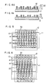
- Fig. 2a is a plan view of a display panel according to the present invention
- Fig. 2b a sectional view taken along the line IIB-IIB in Fig. 2a
- Fig. 2c an enlarged plan view showing the part IIC of the substrate 12 shown in Fig. 2a
- Fig. 2d a sectional view taken along the line IID-IID in Fig. 2c
- Fig. 2e a sectional view taken along the line IIE-IIE in Fig. 2c.
- reference numerals 11 and 12 designate a pair of transparent insulating substrates made of glass, a plastic material or the like for forming a double matrix display panel, 13 and 14 transparent conductive films provided on the substrates 11 and 12 and made of In 2 0 3 , SnO 2 , a mixture of In 2 0 3 and Sn0 2 or the like and 20 a metal contact member provided on a portion of the transparent conductive film 14 which does not correspond to picture elements 40.
- the metal contact member 20 is formed of a first layer 21 which is made of chromium or a chromium alloy, and a second layer 22 which is provided on the first layer 21 and made of nickel or gold.
- a connecting terminal portion 30 to be connected to an external circuit is larger in area than other portions of the metal contact member 20, and has a structure that a third layer 23 made of copper is provided on the second layer 22.
- reference numeral 3 designates a liquid crystal material introduced into a uniform gap (of, for example, 10 ⁇ m) between the substrates 11 and 12, 4 a sealing agent, and 5 an orientation film for the liquid crystal material 3.
- the orientation film 5 is omitted in Figs. 2d and 2e for the sake of brevity.
- One picture element 40 is made up of a pair of facing portions of the transparent conductive films 13 and 14 and a portion of the liquid crystal material situated between the facing portions.
- the present invention is also applicable to the case where the above-mentioned display panel has such a structure as shown in Fig. 3 in place of the structure shown in Fig. 2c, that is, to the case where the transparent conductive film 14 does not exist at a place beneath a portion of the metal contact member 20 for connecting picture elements 40, and therefore this portion of the metal contact member 20 is disposed directly on the substrate 12.
- FIG. 4a An In 2 0 3 film 140 forming a transparent conductive film is deposited through an o evaporation technique, to a thickness of 400 to 500 A, on the transparent insulating substrate 12 which is formed of a glass plate, a plastic film, or the like and has been made clean, and successively a chromium film 210 and a nickel film 220 are deposited through a vacuum evaporation technique and a sputtering technique to form a laminate. It is preferable to successively carry out the above-mentioned steps in the same vacuum evaporation device.
- a first photoresist pattern 91 having the same shape as the metal contact member 20 shown in Fig. 2c is formed, as shown in Fig. 4b.
- the nickel film 220 is chemically etched by using the first photoresist pattern 91 as a mask.
- This etching is carried out at an etching rate of 22 nm/sec using an etching solution at 25°C containing ten volumes of HNO 3 and one volume of H 2 0 2 , or at an etching rate of 8 nm/sec using an etching solution at 25°C containing five volumes of CH 3 COOH, three volumes of HN0 3 , one volume of H 3 PO 4 and one volume of H 2 S0 4 .
- the chromium film 210 is chemically etched at an etching rate of 6.5 nm/sec by using a 25 percent solution of Ce(NO 3 ) ⁇ 2NH 4 NO 3 as an etching solution at 25°C.
- a chromium pattern 21 having the same shape as the metal contact member 20 shown in Fig. 2c is obtained, as shown in Fig. 4d.
- This etching solution produces only a little undercut in the chromium pattern 21, and selectively etches the chromium film 210 without etching the nickel pattern 22 and In 2 0 3 film 140.
- the first photoresist pattern 91 is peeled off by a photoresist removing agent belonging to the xylene group, or the like, as shown in Fig. 4e.
- a second photoresist pattern 92 having the same shape as the transparent conductive film 14 shown in Fig. 2c is formed on the nickel pattern 22 and In 2 0 3 film 140, as shown in Fig. 4f.
- the In203 film 140 is chemically etched by . using the second photoresist pattern 92 as a mask. This etching is carried out at an etching rate of 42 nm/sec using a 47 percent HBr solution as an ethcing solution at 35°C, or at an etching rate of 60 nm/sec using a 57 percent HI solution as an etching solution at 35°C.
- an In 2 0 3 pattern 14 having the same shape as the transparent conductive film 14 shown in Fig. 2c is obtained, as shown in Fig. 4g.
- etching solutions produce only a little undercut in the In 2 0 3 pattern 14, and can selectively etch the In 2 0 3 film 140 without etching the nickel pattern 22 and chromium pattern 21.
- the fabricating cost of the display panel is reduced, since the HBr solution is inexpensive as compared with the HI solution.
- the second photoresist pattern 92 is peeled off by a photoresist removing agent belonging to the xylene group, or the like.
- a desired pattern such as shown in Figs. 2c and 2d is obtained, as shown in Fig. 4h.
- the present inventors have confirmed that the two-layer film of Cr-Ni thus obtained adheres well to the substrate 12 and In 2 O 3 pattern 14 since the lower layer of the two-layer film is formed of the chromium pattern 21, and that the connecting terminal portion of the two-layer film.is readily soldered since the upper layer of the two-layer film is formed of the nickel pattern 22.
- the chromium pattern 21 in the two-layer film of Cr-Ni is required o to have a thickness of more than 250 A to adhere well to the substrate 12 and In 2 0 3 pattern 14. It has been also found that when the thickness of the chromium film 210 is less than 250 A, the chromium film 210 is deposited in such a manner that a number of islands are separately arranged, and therefore the two-layer film of Cr-Ni does not adhere to the substrate 12 and In 2 0 3 pattern 14. However, the thickness of the chromium film 210 should not be made larger than a necessary thickness, since chromium is high in resistivity.
- the most preferable thickness of the chromium pattern 21 o lies in a range between 250 to 1000 A. Further, it has been found that the nickel pattern 22 for reducing the resistance of the two-layer film of Cr-Ni has a sheet o resistivity of 0.8 ⁇ /sq at a thickness of about 1000 A, and the nickel pattern 22 having a thickness of about o 1000 A can exhibit a satisfactory electric characteristic at a fine metal contact member having a width of about 10 ⁇ m.
- the chromium film 210 and nickel film 220 for forming the metal contact member are successively etched by using the first photoresist pattern 91 as a mask, and therefore the number of broken portions in the metal contact member and the number of fabricating steps are small as compared with conventional display panels.
- the chromium film 210 and nickel film 220 for forming the metal contact member and the In 2 0 3 film 140 for forming the transparent conductive film are separately etched by using different photoresist patterns 91 and 92 as respective masks. Accordingly, even when a defect is present in the first photoresist pattern 91 and therefore part of each of the chromium pattern 21 and nickel pattern 22 is broken, there is little danger of an electrode portion which includes the defective metal contact member and the In 2 0 3 pattern 14, being separated into two parts since the In 2 0 3 film 140 is etched by using the second photoresist pattern 92 as a mask.
- the two-layer film of Cr-Ni used as the metal contact member of a matrix liquid crystal display panel adheres well to the substrate and the transparent conductive film, is readily soldered, can be etched with high accuracy through a photoetching technique, and therefore is reliable.
- An In 2 0 3 pattern 14 for forming the transparent conductive film and a two-layer pattern 20 of Cr-Ni for forming the metal contact member are formed in the same manner as EMBODIMENT 1, so as to have a predetermined shape.
- Both ends of an electrode in a liquid crystal display panel are usually used as connecting terminals to be connected to external circuits.
- the present embodiment aims at improving the reliability of soldering at a connecting terminal portion.
- it is required to make large an area getting wet with solder at the connecting terminal portion. It has been found that the reliability of soldering can be improved by forming a copper film 23, which gets wet well with solder as compared with the nickel pattern 22, on the nickel pattern 22 at the connecting terminal portion.
- the Cr-Ni pattern 20 can get wet well with solder by forming the copper film 23 on the pattern 20.
- the copper film 23 can be formed only on the connecting terminal portion of the two-layer pattern 20 of Cr-Ni by various methods such as an_evaporation method and a sputtering method.
- the process for forming the copper.pattern 23 is very simple.
- a liquid crystal material is introduced into a gap between a pair of substrates which have been provided with electrodes. Accordingly, when the peripheral portion of the gap filled with the liquid crystal material has been sealed, only the connecting terminal portion of the Cr-Ni pattern 20 is exposed at end portions of the substrates.
- the copper pattern 23 may be formed by chemical plating in this state. Such a method of forming the copper pattern 23 is very advantageous in simplifying the fabricating process of the display panel, as compared with the case where the copper pattern 23 is formed by the evaporation or sputtering method.
- the metal contact member is formed'of a two-layer film including an NiCr layer and an Au layer, and a copper film is formed on the connecting terminal portion of the metal contact member.
- a two-layer film has advantages that the NiCr layer adheres well to the substrate and In 2 0 3 film, and the Au layer enhances the chemical stability of the two-layer film and is small in electric resistance.
- the connecting terminal portion of the two-layer film and an electric circuit are connected with solder, the Au layer is resolved by solder and therefore a poor connection is made.
- only the connecting terminal portion of the NiCr-Au film is plated with copper, as in EMBODIMENT 2, to prevent the Au layer from being resolved by solder.
- a column electrode pattern is obtained which can be connected perfectly with an electric circuit.
- the thickness of the NiCr layer is made greater than o or equal to 500 A,. and the thickness of the Au layer is not required to be large but is put in a range from 0 500 to 1000 A.
- a two-layer film including a Cr layer and an Au layer is used to form the metal contact member, and a copper film is formed only on the connecting terminal portion of the metal contact member.
- This two-layer film has advantages that the Cr layer adheres well to the substrate and In 2 0 3 film, and the Au layer improves the chemical stability of the two-layer film and is small in electric resistance. Further, the copper film formed on the connecting terminal portion gets wet well with solder, and thus the reliability of soldering is enhanced.
- the present invention is not limited to such a double matrix display panel as shown in Fig. 2a, but is applicable to various multi-matrix display panels such as an inverted double matrix display panel shown in Fig. 5 and an inverted quadruple matrix display panel shown in Fig. 6.
- like reference numerals in Figs. 2a, 5 and 6 designate like or equivalent parts.
- the present invention is not limited to a display panel using a liquid crystal material, but is applicable to display devices using other display substances such as an electroluminescence material and a plasma display material.
Landscapes
- Physics & Mathematics (AREA)
- Nonlinear Science (AREA)
- Engineering & Computer Science (AREA)
- Optics & Photonics (AREA)
- Crystallography & Structural Chemistry (AREA)
- General Physics & Mathematics (AREA)
- Chemical & Material Sciences (AREA)
- Mathematical Physics (AREA)
- Mechanical Engineering (AREA)
- Manufacturing & Machinery (AREA)
- Microelectronics & Electronic Packaging (AREA)
- Liquid Crystal (AREA)
- Devices For Indicating Variable Information By Combining Individual Elements (AREA)
- Electroluminescent Light Sources (AREA)
Abstract
Description
- The present invention relates to display panels such as a liquid crystal display panel and a plasma display panel.
- In display panels, there are used a great variety of display substances which include a liquid crystal material, an electroluminescence material, a plasma display material, and others. A liquid crystal display panel is shown in Fig. 1 of the accompanying drawings, as an example of various display panels.
- Referring to Fig. 1, a pair of substrates 1 and 2 each having an
electrode 5 are disposed with a gap of 5 to 10 µm therebetween. A liquid crystal material is introduced into the gap to form aliquid crystal layer 3, and the peripheral portion of the gap is sealed with asealing agent 4. In this case, each of the substrates 1 and 2 is usually made of glass or a plastic material, and a row electrode and a column electrode are formed on one and the other of the facing surfaces of the substrates, respectively. - In recent years, display devices have been greatly advanced, and it is required to display a great number of characters and pictures on a large panel. In order to satisfy this requirement, a method is used in which a row electrode pattern and a column electrode pattern are made fine to increase the number of picture elements each made up of the row and column electrodes and a display substance (namely, a liquid crystal material) situated therebetween. Further, in order to carry out this method in a satisfactory manner, there is employed a multi-matrix structure that one column electrode is divided into a number of picture element electrodes and one row electrode corresponds to picture element electrodes on a plurality of rows. Please refer to, for example, U.S. Patent No. 4,233,602 and German patent Laid-open No. 2620530. In this structure, however, since a transparent conductive film for forming the picture element electrodes has a high electric resistivity, when a fine electrode pattern is made large in length, an image at that part of the electrode pattern which is apart from a connecting portion connected to an external circuit, becomes dark, or a picture element at such a part may not light up. Thus, irregularities in connection with display are generated, and therefore the picture quality is deteriorated.
- In order to solve this problem, the above-mentioned German patent Laid-open No. 2620530 discloses that a metal contact member of such a low-resistivity material as gold, aluminum or copper is formed on the transparent conductive film. However, the material for forming the metal contact member is required to have high workability in addition to the low resistivity, so that a fine pattern can be formed. Further, it is required that the metal contact member can be connected with en external circuit without arousing any trouble.
- In other words, the metal contact member necessary to form a display panel having a multi-matrix structure is required to satisfy the following conditions, in addition to that the metal contact member has a low electric resistance.
-
- (1) The metal contact member can be readily photo- etched, and can have a desired pattern with high accuracy.
- (2) The metal contact member adheres well to the substrate and the transparent conductive film.
- (3) A connecting terminal portion of the metal contact member can be readily and firmly connected to an electric circuit with solder.
- (4) The metal contact member is high in chemical stability.
- (5) The metal contact member is low in cost, in addition to that the conditions (1) to (4) are satisfied as much as possible.
- It can be readily understood from these conditions how important the material and construction of the metal contact member are in fabricating a display panel having a multi-matrix structure.
- The present inventors have studied the metal contact member from various viewpoints, and have invented a structure of display panel which can satisfy the above-mentioned conditions. The results of the study will be explained below in detail.
- Needless to say, it is desirable that the metal contact member formed of a single-layer film has a low - resistance and can satisfy the above-mentioned conditions. Such metals as aluminum, gold, silver, copper, nickel and chromium have been used to make the single-layer film, as described in, for example, the German patent Laid-open No. 2620530. However, it has been found that the single-layer film made of one of these metals has the following drawbacks.
- A single-layer film made of aluminum can be formed with a pattern with high accuracy, is readily soldered, and adheres well to a transparent conductive film (made of In203 and/or Sn02). However, the transparent conductive film is reduced by hydrogen which is generated in etching the aluminum film, and thus pinholes are produced in the transparent conductive film. Further, after the single-layer film of aluminum has been formed, a fraction of oxygen in the transparent conductive film reacts with aluminum, and thus a swelling is produced in the aluminum pattern. Therefore, the single-layer film made of aluminum is undesirable.
- Further, a single-layer film made of any one of gold, silver and copper does not react with the transparent conductive film, but adheres poorly with the substrate and the transparent conductive film.
- Accordingly, the single-layer film readily peels. In addition, a single-layer film made of gold is easily attacked by solder at the connecting terminal thereof, and therefore it is impossible to connect the film and an external circuit with solder.
- Further, a single-layer film made of nickel can be etched with high accuracy in forming a--fine pattern and is soldered relatively easily, but adheres to the substrate in an unsatisfactory manner. In addition, the soldered joint between the connecting terminal portion of the nickel film and an electric circuit is low in strength, and therefore the connecting terminal portion often peels.
- Further, in addition to the fact that chromium is high in resistivity as compared with the above-mentioned metals, a single-layer film made of chromium gets wet poorly with solder, though the film adheres very well with the substrate and the transparent conductive film. Accordingly, it is impossible to connect the chromium film and an electric circuit with solder.
- It has been made clear from the above-mentioned facts that a metal contact member formed of a single-layer metal film cannot be used in making a multi-matrix structure.
- An object of the present invention is to provide a display panel which can eliminate the drawbacks of the prior art and is provided with an electrode capable of satisfying the above-mentioned conditions (1) to (5) required for an electrode of a matrix liquid crystal display panel.
- In order to attain the above object, according to the present invention, there is provided a display panel which includes a pair of substrates arranged face to face with each other with a predetermined gap therebetween, at least a pair of electrodes each provided on a corresponding one of facing surfaces of the substrates, and a display substance provided between the electrodes, and in which a picture element is made up of a pair of facing portions of the electrodes and a portion of the display substance situated between the facing portions, at least one of the electrodes is made up of a multiplicity of picture element electrodes formed of a transparent conductive film and juxtaposed to each other and a contact metal member for substantially making an electrical connection of a plurality of ones of the picture element electrodes, and the contact metal member is made up of a first layer made of chromium or a chromium alloy and a second layer formed on the first layer and made of nickel or gold.
- The other objects, features and advantages of the present invention will become apparent from the following detailed description of embodiments taken in conjunction with the accompanying drawings, in which:
- Fig. 1 is a schematic view for explaining a fundamental structure of a liquid crystal display panel:
- Fig. 2a is a plan view showing an embodiment of a double matrix liquid crystal display panel, to which the present invention is applicable;
- Fig. 2b is a sectional view taken along the line IIB-IIB in Fig. 2a;
- Fig. 2c is an enlarged plan view showing the part IIC of the
substrate 12 shown in Fig. 2a; - Fig. 2d is a sectional view taken along the line IID-IID in Fig. 2c;
- Fig. 2e is a sectional view taken along the line IIE-IIE in Fig. 2c;
- Fig. 3 is another example of the sectional view taken along the line IID-IID in Fig. 2c;
- Figs. 4a to 4h are views for showing a fabricating process of an embodiment 1 of a display panel according to the present invention;
- Fig. 5 is a plan view showing an embodiment of an inverted double matrix liquid crystal display panel, to which the present invention is applicable; and
- Fig. 6 is a plan view showing an embodiment of an inverted quadruple matrix liquid crystal display panel, to which the present invention is applicable.
- First, a structure of a display panel according to the present invention will be explained below in detail, with reference to Figs. 2a to 2e. Fig. 2a is a plan view of a display panel according to the present invention, Fig. 2b a sectional view taken along the line IIB-IIB in Fig. 2a, Fig. 2c an enlarged plan view showing the part IIC of the
substrate 12 shown in Fig. 2a, Fig. 2d a sectional view taken along the line IID-IID in Fig. 2c, and Fig. 2e a sectional view taken along the line IIE-IIE in Fig. 2c. - In Figs. 2a to 2e,
reference numerals 11 and 12 designate a pair of transparent insulating substrates made of glass, a plastic material or the like for forming a double matrix display panel, 13 and 14 transparent conductive films provided on thesubstrates 11 and 12 and made of In203, SnO2, a mixture of In203 and Sn02 or the like and 20 a metal contact member provided on a portion of the transparentconductive film 14 which does not correspond to pictureelements 40. Themetal contact member 20 is formed of afirst layer 21 which is made of chromium or a chromium alloy, and asecond layer 22 which is provided on thefirst layer 21 and made of nickel or gold. A connectingterminal portion 30 to be connected to an external circuit is larger in area than other portions of themetal contact member 20, and has a structure that athird layer 23 made of copper is provided on thesecond layer 22. Further,reference numeral 3 designates a liquid crystal material introduced into a uniform gap (of, for example, 10 µm) between thesubstrates 11 and 12, 4 a sealing agent, and 5 an orientation film for theliquid crystal material 3. Theorientation film 5 is omitted in Figs. 2d and 2e for the sake of brevity. Onepicture element 40 is made up of a pair of facing portions of the transparentconductive films - Further, the present invention is also applicable to the case where the above-mentioned display panel has such a structure as shown in Fig. 3 in place of the structure shown in Fig. 2c, that is, to the case where the transparent
conductive film 14 does not exist at a place beneath a portion of themetal contact member 20 for connectingpicture elements 40, and therefore this portion of themetal contact member 20 is disposed directly on thesubstrate 12. - Now, various embodiments of a display panel according to the present invention will be explained on the basis of the above-mentioned structures.
- A process for fabricating the present embodiment will be first described with reference to Figs. 4a to 4h. Referring to Fig. 4a, an In203
film 140 forming a transparent conductive film is deposited through an o evaporation technique, to a thickness of 400 to 500 A, on the transparent insulatingsubstrate 12 which is formed of a glass plate, a plastic film, or the like and has been made clean, and successively achromium film 210 and anickel film 220 are deposited through a vacuum evaporation technique and a sputtering technique to form a laminate. It is preferable to successively carry out the above-mentioned steps in the same vacuum evaporation device. - Next, a
first photoresist pattern 91 having the same shape as themetal contact member 20 shown in Fig. 2c is formed, as shown in Fig. 4b. - Then, the
nickel film 220 is chemically etched by using thefirst photoresist pattern 91 as a mask. - This etching is carried out at an etching rate of 22 nm/sec using an etching solution at 25°C containing ten volumes of HNO3 and one volume of H202, or at an etching rate of 8 nm/sec using an etching solution at 25°C containing five volumes of CH3COOH, three volumes of HN03, one volume of H3PO4 and one volume of H2S04.
- Thus, a
nickel pattern 22 having the same shape as themetal contact member 20 shown in Fig. 2c is obtained, as shown in Fig. 4c. These etching solutions produce only a little undercut in thenickel pattern 22. - Next, the
chromium film 210 is chemically etched at an etching rate of 6.5 nm/sec by using a 25 percent solution of Ce(NO3)·2NH4NO3 as an etching solution at 25°C. Thus, achromium pattern 21 having the same shape as themetal contact member 20 shown in Fig. 2c is obtained, as shown in Fig. 4d. This etching solution produces only a little undercut in thechromium pattern 21, and selectively etches thechromium film 210 without etching thenickel pattern 22 and In203film 140. - Next, the
first photoresist pattern 91 is peeled off by a photoresist removing agent belonging to the xylene group, or the like, as shown in Fig. 4e. - Then, a
second photoresist pattern 92 having the same shape as the transparentconductive film 14 shown in Fig. 2c is formed on thenickel pattern 22 and In203film 140, as shown in Fig. 4f. - The
In203 film 140 is chemically etched by . using thesecond photoresist pattern 92 as a mask. This etching is carried out at an etching rate of 42 nm/sec using a 47 percent HBr solution as an ethcing solution at 35°C, or at an etching rate of 60 nm/sec using a 57 percent HI solution as an etching solution at 35°C. Thus, an In203pattern 14 having the same shape as the transparentconductive film 14 shown in Fig. 2c is obtained, as shown in Fig. 4g. These etching solutions produce only a little undercut in the In203pattern 14, and can selectively etch the In203film 140 without etching thenickel pattern 22 andchromium pattern 21. When the HBr solution is employed, the fabricating cost of the display panel is reduced, since the HBr solution is inexpensive as compared with the HI solution. - Next, the
second photoresist pattern 92 is peeled off by a photoresist removing agent belonging to the xylene group, or the like. Thus, a desired pattern such as shown in Figs. 2c and 2d is obtained, as shown in Fig. 4h. - The present inventors have confirmed that the two-layer film of Cr-Ni thus obtained adheres well to the
substrate 12 and In2O3 pattern 14 since the lower layer of the two-layer film is formed of thechromium pattern 21, and that the connecting terminal portion of the two-layer film.is readily soldered since the upper layer of the two-layer film is formed of thenickel pattern 22. - Further, it has been found that the
chromium pattern 21 in the two-layer film of Cr-Ni is required o to have a thickness of more than 250 A to adhere well to thesubstrate 12 and In203pattern 14. It has been also found that when the thickness of thechromium film 210 is less than 250 A, thechromium film 210 is deposited in such a manner that a number of islands are separately arranged, and therefore the two-layer film of Cr-Ni does not adhere to thesubstrate 12 and In203pattern 14. However, the thickness of thechromium film 210 should not be made larger than a necessary thickness, since chromium is high in resistivity. Thus, the most preferable thickness of the chromium pattern 21 o lies in a range between 250 to 1000 A. Further, it has been found that thenickel pattern 22 for reducing the resistance of the two-layer film of Cr-Ni has a sheet o resistivity of 0.8 Ω/sq at a thickness of about 1000 A, and thenickel pattern 22 having a thickness of about o 1000 A can exhibit a satisfactory electric characteristic at a fine metal contact member having a width of about 10 µm. - In the present embodiment, the
chromium film 210 andnickel film 220 for forming the metal contact member are successively etched by using thefirst photoresist pattern 91 as a mask, and therefore the number of broken portions in the metal contact member and the number of fabricating steps are small as compared with conventional display panels. - Further, the
chromium film 210 andnickel film 220 for forming the metal contact member and the In203film 140 for forming the transparent conductive film are separately etched by usingdifferent photoresist patterns first photoresist pattern 91 and therefore part of each of thechromium pattern 21 andnickel pattern 22 is broken, there is little danger of an electrode portion which includes the defective metal contact member and the In203pattern 14, being separated into two parts since the In203film 140 is etched by using thesecond photoresist pattern 92 as a mask. - As is evident from the above-mentioned description, the two-layer film of Cr-Ni used as the metal contact member of a matrix liquid crystal display panel adheres well to the substrate and the transparent conductive film, is readily soldered, can be etched with high accuracy through a photoetching technique, and therefore is reliable.
- An In203
pattern 14 for forming the transparent conductive film and a two-layer pattern 20 of Cr-Ni for forming the metal contact member are formed in the same manner as EMBODIMENT 1, so as to have a predetermined shape. - Both ends of an electrode in a liquid crystal display panel are usually used as connecting terminals to be connected to external circuits. The present embodiment aims at improving the reliability of soldering at a connecting terminal portion. In order to improve the reliability of soldering, it is required to make large an area getting wet with solder at the connecting terminal portion. It has been found that the reliability of soldering can be improved by forming a
copper film 23, which gets wet well with solder as compared with thenickel pattern 22, on thenickel pattern 22 at the connecting terminal portion. In more detail, in both of the case where thecopper film 23 was not formed on the connecting terminal portion of the Cr-Ni pattern 20 and the case where thecopper film 23 was formed on the connecting terminal portion, it was measured how much the connecting terminal portion got wet with solder, and it was found that 80 percent of the connecting terminal portion having no copper film got wet with solder and 100 percent of the connecting terminal portion having thecopper film 23 got wet with solder. That is, the Cr-Ni pattern 20 can get wet well with solder by forming thecopper film 23 on thepattern 20. Thecopper film 23 can be formed only on the connecting terminal portion of the two-layer pattern 20 of Cr-Ni by various methods such as an_evaporation method and a sputtering method. However, it is evident that chemical plating is most suited to form thecopper film 23 on the connecting terminal portion. In more detail, when thecopper pattern 23 is formed by the evaporation method or the- sputtering method, evaporation or sputtering has to be carried out while using a mask, or thecopper film 23 which has been formed by one of these methods, must be etched through a photoresist technique. That is, these processes for forming thecopper pattern 23 are complicated. On the other hand, in the case where thecopper pattern 23 is formed by chemical plating, a copper layer having a desired thickness can be obtained by dipping only the connecting terminal portion of the two-layer pattern 20 of Cr-Ni into a plating bath. - That is, the process for forming the
copper.pattern 23 is very simple. - When a liquid crystal display panel is fabricated, a liquid crystal material is introduced into a gap between a pair of substrates which have been provided with electrodes. Accordingly, when the peripheral portion of the gap filled with the liquid crystal material has been sealed, only the connecting terminal portion of the Cr-
Ni pattern 20 is exposed at end portions of the substrates. Thecopper pattern 23 may be formed by chemical plating in this state. Such a method of forming thecopper pattern 23 is very advantageous in simplifying the fabricating process of the display panel, as compared with the case where thecopper pattern 23 is formed by the evaporation or sputtering method. - In this embodiment, the metal contact member is formed'of a two-layer film including an NiCr layer and an Au layer, and a copper film is formed on the connecting terminal portion of the metal contact member. Such a two-layer film has advantages that the NiCr layer adheres well to the substrate and In203 film, and the Au layer enhances the chemical stability of the two-layer film and is small in electric resistance. However, when the connecting terminal portion of the two-layer film and an electric circuit are connected with solder, the Au layer is resolved by solder and therefore a poor connection is made. Accordingly, in the present embodiment, only the connecting terminal portion of the NiCr-Au film is plated with copper, as in EMBODIMENT 2, to prevent the Au layer from being resolved by solder. Thus, a column electrode pattern is obtained which can be connected perfectly with an electric circuit.
- In the NiCr-Au film of the present embodiment, the thickness of the NiCr layer is made greater than o or equal to 500 A,. and the thickness of the Au layer is not required to be large but is put in a range from 0 500 to 1000 A.
- In this embodiment, a two-layer film including a Cr layer and an Au layer is used to form the metal contact member, and a copper film is formed only on the connecting terminal portion of the metal contact member. This two-layer film has advantages that the Cr layer adheres well to the substrate and In203 film, and the Au layer improves the chemical stability of the two-layer film and is small in electric resistance. Further, the copper film formed on the connecting terminal portion gets wet well with solder, and thus the reliability of soldering is enhanced.
- The present invention is not limited to such a double matrix display panel as shown in Fig. 2a, but is applicable to various multi-matrix display panels such as an inverted double matrix display panel shown in Fig. 5 and an inverted quadruple matrix display panel shown in Fig. 6. Incidentally, like reference numerals in Figs. 2a, 5 and 6 designate like or equivalent parts.
- Further, the present invention is not limited to a display panel using a liquid crystal material, but is applicable to display devices using other display substances such as an electroluminescence material and a plasma display material.
Claims (6)
Applications Claiming Priority (2)
| Application Number | Priority Date | Filing Date | Title |
|---|---|---|---|
| JP46504/81 | 1981-03-31 | ||
| JP56046504A JPS57161882A (en) | 1981-03-31 | 1981-03-31 | Display body panel |
Publications (2)
| Publication Number | Publication Date |
|---|---|
| EP0062289A2 true EP0062289A2 (en) | 1982-10-13 |
| EP0062289A3 EP0062289A3 (en) | 1984-04-04 |
Family
ID=12749071
Family Applications (1)
| Application Number | Title | Priority Date | Filing Date |
|---|---|---|---|
| EP82102685A Withdrawn EP0062289A3 (en) | 1981-03-31 | 1982-03-30 | Display panel |
Country Status (3)
| Country | Link |
|---|---|
| US (1) | US4543573A (en) |
| EP (1) | EP0062289A3 (en) |
| JP (1) | JPS57161882A (en) |
Cited By (5)
| Publication number | Priority date | Publication date | Assignee | Title |
|---|---|---|---|---|
| FR2581783A1 (en) * | 1985-05-07 | 1986-11-14 | Commissariat Energie Atomique | ACTIVE MATRIX DISPLAY DEVICE WITH INTEGRATED CONTROL COMPRISING TWO FAMILIES OF LINEAR ELECTRODES AND TWO FAMILIES OF COLLECTED ELECTRODES BY IMAGE POINT AND ITS CONTROL METHOD |
| EP0344367A1 (en) * | 1988-05-03 | 1989-12-06 | Copytele Inc. | Monolithic flat panel display apparatus |
| EP0444580A3 (en) * | 1990-02-26 | 1992-03-11 | Canon Kabushiki Kaisha | Liquid crystal device and display apparatus |
| US5146301A (en) * | 1987-10-15 | 1992-09-08 | Sharp Kabushiki Kaisha | Terminal electrode structure of a liquid crystal panel display |
| EP0495632A3 (en) * | 1991-01-14 | 1993-01-20 | Sharp Kabushiki Kaisha | Liquid crystal display |
Families Citing this family (23)
| Publication number | Priority date | Publication date | Assignee | Title |
|---|---|---|---|---|
| US5365079A (en) * | 1982-04-30 | 1994-11-15 | Seiko Epson Corporation | Thin film transistor and display device including same |
| US5677547A (en) * | 1982-04-30 | 1997-10-14 | Seiko Epson Corporation | Thin film transistor and display device including same |
| US5650637A (en) * | 1982-04-30 | 1997-07-22 | Seiko Epson Corporation | Active matrix assembly |
| US4642620A (en) * | 1982-09-27 | 1987-02-10 | Citizen Watch Company Limited | Matrix display device |
| JPS59170881A (en) * | 1983-03-17 | 1984-09-27 | セイコーインスツルメンツ株式会社 | Formation of electrode for liquid crystal panel |
| FR2585167B1 (en) * | 1985-07-19 | 1993-05-07 | Gen Electric | REDUNDANT CONDUCTIVE STRUCTURES FOR LIQUID CRYSTAL DISPLAYS CONTROLLED BY THIN FILM FIELD EFFECT TRANSISTORS |
| FR2602362B1 (en) * | 1986-08-01 | 1988-10-07 | Commissariat Energie Atomique | MATRIX DISPLAY DEVICE COMPRISING TWO PACKS OF LINEAR ELECTRODES AND TWO COLUMNED ELECTRODES BY IMAGE ELEMENT AND ITS DRIVING METHOD |
| EP0478621A4 (en) * | 1989-06-17 | 1993-02-03 | William F. Glick | Color display system using thin film color control |
| US5153754A (en) * | 1989-06-30 | 1992-10-06 | General Electric Company | Multi-layer address lines for amorphous silicon liquid crystal display devices |
| JP3009438B2 (en) * | 1989-08-14 | 2000-02-14 | 株式会社日立製作所 | Liquid crystal display |
| JPH03125443A (en) * | 1989-10-09 | 1991-05-28 | Sharp Corp | Electrode of mounting board and liquid crystal display having the electrode of this mounting board |
| US5498573A (en) * | 1989-11-29 | 1996-03-12 | General Electric Company | Method of making multi-layer address lines for amorphous silicon liquid crystal display devices |
| JP2652072B2 (en) * | 1990-02-26 | 1997-09-10 | キヤノン株式会社 | Method of forming light-shielding layer |
| NL9000545A (en) * | 1990-03-09 | 1991-10-01 | Philips Nv | METHOD FOR PRODUCING CONDUCTOR RAILS |
| JP2680730B2 (en) * | 1990-09-17 | 1997-11-19 | シャープ株式会社 | Thin film EL panel |
| JP2952075B2 (en) * | 1991-06-12 | 1999-09-20 | キヤノン株式会社 | Liquid crystal device manufacturing method |
| US5515191A (en) * | 1994-05-31 | 1996-05-07 | Motorola, Inc. | Liquid crystal display having enhanced conductors and adhesive spacers |
| US6106907A (en) | 1996-06-25 | 2000-08-22 | Canon Kabushiki Kaisha | Electrode plate, liquid crystal device and production thereof |
| US6008877A (en) * | 1996-11-28 | 1999-12-28 | Sharp Kabushiki Kaisha | Liquid crystal display having multilayered electrodes with a layer adhesive to a substrate formed of indium tin oxide |
| JP3617458B2 (en) * | 2000-02-18 | 2005-02-02 | セイコーエプソン株式会社 | Substrate for display device, liquid crystal device and electronic device |
| KR100690001B1 (en) * | 2000-02-21 | 2007-03-08 | 엘지.필립스 엘시디 주식회사 | LCD and its manufacturing method |
| JP4098049B2 (en) * | 2001-11-30 | 2008-06-11 | シャープ株式会社 | Display panel |
| CN104795407B (en) * | 2015-04-23 | 2016-02-24 | 京东方科技集团股份有限公司 | A kind of array base palte and preparation method thereof, display floater, display unit |
Family Cites Families (10)
| Publication number | Priority date | Publication date | Assignee | Title |
|---|---|---|---|---|
| US3483610A (en) * | 1967-06-08 | 1969-12-16 | Bell Telephone Labor Inc | Thermocompression bonding of foil leads |
| NL163370C (en) * | 1972-04-28 | 1980-08-15 | Philips Nv | METHOD FOR MANUFACTURING A SEMI-CONDUCTOR DEVICE WITH A CONDUCTOR PATTERN |
| AT323249B (en) * | 1972-07-03 | 1975-06-25 | Electrovac | LIQUID CRYSTAL CELL |
| CH557071A (en) * | 1973-09-07 | 1974-12-13 | Bbc Brown Boveri & Cie | METHOD FOR MANUFACTURING LIQUID CRYSTAL CELLS, AFTER-MANUFACTURING LIQUID CRYSTAL CELLS AND APPLICATION OF LIQUID CRYSTAL CELLS AS DISPLAY ELEMENTS. |
| US4231640A (en) * | 1977-07-07 | 1980-11-04 | Sharp Kabushiki Kaisha | Matrix type liquid crystal display panel |
| JPS5846454Y2 (en) * | 1977-11-10 | 1983-10-22 | シャープ株式会社 | Electrode structure of liquid crystal display device |
| JPS556346A (en) * | 1978-06-27 | 1980-01-17 | Sharp Kk | Electrode pattern and method of forming same |
| JPS5559490A (en) * | 1978-10-26 | 1980-05-02 | Citizen Watch Co Ltd | Liquid crystal display cell having double layer electrode structure |
| US4362903A (en) * | 1980-12-29 | 1982-12-07 | General Electric Company | Electrical conductor interconnect providing solderable connections to hard-to-contact substrates, such as liquid crystal cells |
| DE3136794C2 (en) * | 1981-09-16 | 1983-07-28 | Siemens AG, 1000 Berlin und 8000 München | Solderable layer system, its use and process for its production |
-
1981
- 1981-03-31 JP JP56046504A patent/JPS57161882A/en active Granted
-
1982
- 1982-03-30 EP EP82102685A patent/EP0062289A3/en not_active Withdrawn
- 1982-03-30 US US06/363,458 patent/US4543573A/en not_active Expired - Fee Related
Cited By (10)
| Publication number | Priority date | Publication date | Assignee | Title |
|---|---|---|---|---|
| FR2581783A1 (en) * | 1985-05-07 | 1986-11-14 | Commissariat Energie Atomique | ACTIVE MATRIX DISPLAY DEVICE WITH INTEGRATED CONTROL COMPRISING TWO FAMILIES OF LINEAR ELECTRODES AND TWO FAMILIES OF COLLECTED ELECTRODES BY IMAGE POINT AND ITS CONTROL METHOD |
| EP0202992A1 (en) * | 1985-05-07 | 1986-11-26 | Commissariat A L'energie Atomique | Active matrix display device with integrated control |
| US4753518A (en) * | 1985-05-07 | 1988-06-28 | Commissariat A L'energie Atomique | Integrated control, active matrix display comprising two groups of row electrodes and two groups of column electrodes per image point and its control process |
| US5146301A (en) * | 1987-10-15 | 1992-09-08 | Sharp Kabushiki Kaisha | Terminal electrode structure of a liquid crystal panel display |
| EP0344367A1 (en) * | 1988-05-03 | 1989-12-06 | Copytele Inc. | Monolithic flat panel display apparatus |
| EP0444580A3 (en) * | 1990-02-26 | 1992-03-11 | Canon Kabushiki Kaisha | Liquid crystal device and display apparatus |
| US5150233A (en) * | 1990-02-26 | 1992-09-22 | Canon Kabushiki Kaisha | Liquid crystal device and display apparatus with a three-layered electrode of ito, molybdenum, and aluminum |
| US5543946A (en) * | 1990-02-26 | 1996-08-06 | Canon Kabushiki Kaisha | Liquid crystal device and display apparatus with multilayer electrodes |
| EP0495632A3 (en) * | 1991-01-14 | 1993-01-20 | Sharp Kabushiki Kaisha | Liquid crystal display |
| US5274483A (en) * | 1991-01-14 | 1993-12-28 | Sharp Kabushiki Kaisha | Liquid crystal display with conductive film along the edge of electrodes of one substrate and between dot electrodes of the other substrate |
Also Published As
| Publication number | Publication date |
|---|---|
| US4543573A (en) | 1985-09-24 |
| JPS6219756B2 (en) | 1987-04-30 |
| JPS57161882A (en) | 1982-10-05 |
| EP0062289A3 (en) | 1984-04-04 |
Similar Documents
| Publication | Publication Date | Title |
|---|---|---|
| US4543573A (en) | Display panel | |
| EP0226997A2 (en) | Liquid crystal display device | |
| US4964947A (en) | Method of manufacturing double-sided wiring substrate | |
| JP4592875B2 (en) | Flexible wiring board, manufacturing method thereof, and display device | |
| EP0487055B1 (en) | Matrix array substrate | |
| JPH0239044B2 (en) | ||
| JPH02281237A (en) | Electrode structure of display device | |
| JP4590527B2 (en) | Thin film electrode substrate manufacturing method | |
| US20030173106A1 (en) | Method for manufacturing transparent conductive panels with a low contact surface impedance | |
| JPH08185978A (en) | EL display and manufacturing method thereof | |
| JPH02272774A (en) | Active matrix circuit board | |
| JPH11297751A (en) | Semiconductor device | |
| JPS60161686A (en) | Manufacture of thin film non-linear device | |
| JPS58137908A (en) | Method of forming transparent electrode | |
| JPS609273B2 (en) | display device | |
| JP2590094B2 (en) | LCD module | |
| JPH07304Y2 (en) | Mask for solder paste printing | |
| JPH07244295A (en) | Liquid crystal display device and manufacturing method thereof | |
| JPS61133979A (en) | Electrode construction of display element | |
| JPS62218939A (en) | Production of liquid crystal display device | |
| EP0393851A1 (en) | A method of manufacturing a non-linear resistive element array | |
| JPH02924A (en) | Manufacture of nonlinear resistance element | |
| JP2845929B2 (en) | Manufacturing method of nonlinear element | |
| JPS6364081A (en) | Formation of wire electrode | |
| JPH01287990A (en) | Electrode formation method |
Legal Events
| Date | Code | Title | Description |
|---|---|---|---|
| PUAI | Public reference made under article 153(3) epc to a published international application that has entered the european phase |
Free format text: ORIGINAL CODE: 0009012 |
|
| AK | Designated contracting states |
Designated state(s): CH DE FR GB IT NL SE |
|
| 17P | Request for examination filed |
Effective date: 19830208 |
|
| PUAL | Search report despatched |
Free format text: ORIGINAL CODE: 0009013 |
|
| AK | Designated contracting states |
Designated state(s): CH DE FR GB IT LI NL SE |
|
| STAA | Information on the status of an ep patent application or granted ep patent |
Free format text: STATUS: THE APPLICATION HAS BEEN WITHDRAWN |
|
| 18W | Application withdrawn |
Withdrawal date: 19860502 |
|
| RIN1 | Information on inventor provided before grant (corrected) |
Inventor name: FUYAMA, MORIAKI Inventor name: SAWAHATA, MAMORU Inventor name: MORIJIRI, MAKOTO Inventor name: HACHINO, HIROAKI Inventor name: TAMURA, KATSUMI |