EP0062295A1 - Digitales Koppelfeld - Google Patents
Digitales Koppelfeld Download PDFInfo
- Publication number
- EP0062295A1 EP0062295A1 EP82102709A EP82102709A EP0062295A1 EP 0062295 A1 EP0062295 A1 EP 0062295A1 EP 82102709 A EP82102709 A EP 82102709A EP 82102709 A EP82102709 A EP 82102709A EP 0062295 A1 EP0062295 A1 EP 0062295A1
- Authority
- EP
- European Patent Office
- Prior art keywords
- links
- control
- phase
- terminal
- unité
- Prior art date
- Legal status (The legal status is an assumption and is not a legal conclusion. Google has not performed a legal analysis and makes no representation as to the accuracy of the status listed.)
- Granted
Links
- 239000003550 marker Substances 0.000 claims abstract description 33
- 230000001360 synchronised effect Effects 0.000 claims abstract description 8
- 230000015654 memory Effects 0.000 claims description 63
- 238000012360 testing method Methods 0.000 claims description 14
- 230000005540 biological transmission Effects 0.000 claims description 12
- 238000002347 injection Methods 0.000 claims description 8
- 239000007924 injection Substances 0.000 claims description 8
- 238000010200 validation analysis Methods 0.000 claims description 8
- 238000006243 chemical reaction Methods 0.000 claims description 7
- 238000005070 sampling Methods 0.000 claims description 7
- 238000004891 communication Methods 0.000 claims description 5
- 230000002457 bidirectional effect Effects 0.000 claims description 2
- 102100040565 Dynein light chain 1, cytoplasmic Human genes 0.000 description 22
- 101000966403 Homo sapiens Dynein light chain 1, cytoplasmic Proteins 0.000 description 22
- 102100025477 GTP-binding protein Rit1 Human genes 0.000 description 13
- 101000574654 Homo sapiens GTP-binding protein Rit1 Proteins 0.000 description 13
- 230000006870 function Effects 0.000 description 9
- 238000010586 diagram Methods 0.000 description 8
- 238000006677 Appel reaction Methods 0.000 description 6
- 235000021183 entrée Nutrition 0.000 description 6
- 238000013519 translation Methods 0.000 description 6
- 102100029820 Mitochondrial brown fat uncoupling protein 1 Human genes 0.000 description 5
- 230000003321 amplification Effects 0.000 description 5
- 238000003199 nucleic acid amplification method Methods 0.000 description 5
- 238000012546 transfer Methods 0.000 description 5
- 102100027778 GTP-binding protein Rit2 Human genes 0.000 description 4
- 101000725879 Homo sapiens GTP-binding protein Rit2 Proteins 0.000 description 4
- 238000004458 analytical method Methods 0.000 description 4
- 238000000034 method Methods 0.000 description 4
- 238000013475 authorization Methods 0.000 description 3
- 101100222094 Arabidopsis thaliana CSP4 gene Proteins 0.000 description 2
- 101150020532 CPS4 gene Proteins 0.000 description 2
- 101100126625 Caenorhabditis elegans itr-1 gene Proteins 0.000 description 2
- 102100027557 Calcipressin-1 Human genes 0.000 description 2
- 101000855412 Homo sapiens Carbamoyl-phosphate synthase [ammonia], mitochondrial Proteins 0.000 description 2
- 101000983292 Homo sapiens N-fatty-acyl-amino acid synthase/hydrolase PM20D1 Proteins 0.000 description 2
- 101100247605 Homo sapiens RCAN1 gene Proteins 0.000 description 2
- 101000861263 Homo sapiens Steroid 21-hydroxylase Proteins 0.000 description 2
- 108010050258 Mitochondrial Uncoupling Proteins Proteins 0.000 description 2
- 102100026873 N-fatty-acyl-amino acid synthase/hydrolase PM20D1 Human genes 0.000 description 2
- 240000008042 Zea mays Species 0.000 description 2
- 101150064416 csp1 gene Proteins 0.000 description 2
- 238000001914 filtration Methods 0.000 description 2
- 230000002093 peripheral effect Effects 0.000 description 2
- 230000011664 signaling Effects 0.000 description 2
- 239000000243 solution Substances 0.000 description 2
- 238000011144 upstream manufacturing Methods 0.000 description 2
- 101100322245 Caenorhabditis elegans des-2 gene Proteins 0.000 description 1
- 102100026191 Class E basic helix-loop-helix protein 40 Human genes 0.000 description 1
- 101710130550 Class E basic helix-loop-helix protein 40 Proteins 0.000 description 1
- 102100026190 Class E basic helix-loop-helix protein 41 Human genes 0.000 description 1
- 101000765033 Homo sapiens Class E basic helix-loop-helix protein 41 Proteins 0.000 description 1
- 241001080024 Telles Species 0.000 description 1
- 238000001514 detection method Methods 0.000 description 1
- 238000011161 development Methods 0.000 description 1
- 238000005516 engineering process Methods 0.000 description 1
- 239000000463 material Substances 0.000 description 1
- 239000011159 matrix material Substances 0.000 description 1
- 210000000056 organ Anatomy 0.000 description 1
- 230000004044 response Effects 0.000 description 1
- IOVGROKTTNBUGK-SJCJKPOMSA-N ritodrine Chemical compound N([C@@H](C)[C@H](O)C=1C=CC(O)=CC=1)CCC1=CC=C(O)C=C1 IOVGROKTTNBUGK-SJCJKPOMSA-N 0.000 description 1
- 230000002123 temporal effect Effects 0.000 description 1
Images



Classifications
-
- H—ELECTRICITY
- H04—ELECTRIC COMMUNICATION TECHNIQUE
- H04M—TELEPHONIC COMMUNICATION
- H04M3/00—Automatic or semi-automatic exchanges
- H04M3/22—Arrangements for supervision, monitoring or testing
- H04M3/24—Arrangements for supervision, monitoring or testing with provision for checking the normal operation
- H04M3/244—Arrangements for supervision, monitoring or testing with provision for checking the normal operation for multiplex systems
-
- H—ELECTRICITY
- H04—ELECTRIC COMMUNICATION TECHNIQUE
- H04Q—SELECTING
- H04Q11/00—Selecting arrangements for multiplex systems
- H04Q11/04—Selecting arrangements for multiplex systems for time-division multiplexing
Definitions
- the invention relates to a digital connection network for a central office comprising a distributed structure control unit. It is applicable in the telecommunications and telematics industries, in particular in time-based automatic exchanges.
- Multi-stage connection networks are described in French patents n ° 69 16790, 70 33 980, 71 04655. Attempts have also been made to improve modularity, to optimize the equipment installed and facilitate extensions, and reliability, to limit urgent interventions. This was obtained by improvements in internal structures, for example according to French patents n ° 69 16790 and 78 30715, and by organizational improvements concerning the possibilities of mutual assistance or switching to emergency units with redundancy of the material as reduced as possible, for example according to French patent n ° 78 18221.
- the object of the invention is therefore to provide a simple, modular, self-controlled connection network.
- the simplicity allows a strong redundancy for a low additional cost, which increases the reliability of the network and reduces urgent interventions in the very rare cases of multiple failures on all the redundant organs.
- the object of the invention is a digital connection network for a PABX comprising a distributed structure control assembly and a central network to which are connected by multiplex links, terminal units themselves comprising means for connecting the terminals to said terminals.
- links, the central network being divided into several independent planes, characterized in that each plan consists of synchronized switches each equipped with a marker, and forming a single switching stage, the switches being connected in parallel to the incoming links of the plan and each serving a group of outgoing links.
- Each multiplex link serves in parallel several terminal units forming a group, each group being connected by at least one link to each plane of the central network.
- the link has five pairs of wires to each station connected for the call, authorization, clock, send and receive functions.
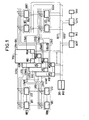
- the links between the control units UC and the terminal units UT are made in the connection network by means of semi-permanent connections established between the channels MIC.
- the central connection network RXA to RXD is controlled by markers MQ1 to MQd controlled by the control units UC also via the links RIT1, RIT2.
- All the units mentioned above UT, UC, UCP, MQ have an HDLC type transmission / reception circuit for messages, for example a MC 6854 type circuit from the company MOTOROLA or 8273 from the company INTEL.
- Each subscriber terminal T1 to Tp is formed of a line circuit CL, comprising power supply, protection, loop supervision and of ringing injection, and of an analog / digital coding filtering and coding FCD circuit.
- the UT terminal unit is controlled by an mP microprocessor connected to the LX multiplex links here four in number by an HDLC transceiver circuit.
- the switching stage is in this example an MCX switching matrix of the spatial type.
- the time switch is performed at the filtering and coding circuits FCD by synchronization on the chosen channel, under the control of the microprocessor. This also controls the line circuits CL via an IS interface for supervision and control.
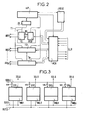
- the central connection network is detailed in Figure 3. It has a single switching stage and is organized into four independent planes. Each connection network plan has a capacity of 128 bidirectional LX multiplex links, i.e. it can connect any channel from one of the 128 incoming LE links to any channel from any of the 128 links outgoing LS.
- a connection network plan includes four switches CX1 to CX4 each equipped with a marker MQ1 to MD4 and with a capacity of 128 incoming links LE and 32 outgoing links LS.
- the LE links are therefore multiplied on the four switches of the plane.
- the structure of a switch CX is shown in FIG. 4.
- the 128 lines LE are distributed over four input amplification circuits CAE1 to CAE4 each comprising 32 AF amplifiers and a synchronization circuit SYN.
- the CAE input amplification circuits are common to the four CX switches on the same plane and each serve 32 of the 128 LE links leading to this plane.
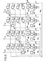
- Each input amplifier circuit CAE is connected to one of the buffer memory circuits CMT1 to CMT4, in each switch CX, these circuits constituting square connection matrices and each comprising successively an input control circuit by sampling CE, a series-parallel conversion circuit CSP, and an access circuit CA to a buffer memory MT.
- the access circuit CA also allows the injection of samples for a so-called "active" control of the connection network.
- the memory MT comprises 1024 words of 8 eb, that is to say a word per channel of the 32 LE lines concerned, and the input-output rate..of the memory is 8 MHz, that is to say a bit rate close to the maximum allowed with the TTL technology used.
- the addressing is of the "downstream command" type, that is to say it is supplied in writing by a counter CR and in reading by a control circuit CMC controlled by the marker MQ.
- the control memory MC supplies the reading address of the memories MT of the four buffer memory circuits CMT1 to CMT4, it is itself addressed cyclically in reading and by the writing marker in order to allow the recording of each new connection. or logout.
- the marker MQ comprises an microprocessor mPC which is connected to the links RIT1, RIT2 by access circuits AR1, AR2. described later.
- the outputs of the buffer memories MT of the four buffer memory circuits CMT1 to CMT4 of a plane are connected in parallel to an output amplification circuit CAS comprising buffer registers R, connected to a parallel conversion circuit - series CPS itself- even connected to an output sampling circuit CS serving a group of 32 amplifiers AS each connected to a different outgoing link LS.
- the set of clock signals HR1 to HRq necessary for the operation of the switch is supplied by a signal distribution module MD controlled by oscillators 01 to Od not shown in the automatic switch.
- the CMT buffer and CAS output amplifier circuits are shown in Figures 6A and 6B, respectively.
- the clock and synchronization signals are distributed by a time base circuit BT1 which is itself synchronized with the signal distribution module MD of the switch (FIG. 4).
- the circuit BT1 delivers signals "h" which will not be described in detail since they are in the field of known art, and they arise from the operation of the circuits, as described below.
- the signal "ce” is taken from the thirty two links LE of the time switch is carried out by means of a multiplexer MX1 individually connected to the thirty two links and the address "ACE" of the link to be controlled is supplied by the CMC circuit of this CX switch.
- the conversion circuit CSP is formed by four integrated circuits CSP1 to CSP4 of the "MICSPA" type each connected to eight of the 32 incoming links of the buffer memory circuit CMT via as many P gates.
- the outputs of the circuits CSP1 to CSP4 are respectively connected to four registers R1 to R4.
- the routing of the samples to the buffer memory is carried out by a multiplexer MX2, an input of which is assigned to the injection of an active control code "Ca" marked for example by wiring.
- Gates of type "AND" generally referenced P which are validated by the time base BT1 control the entry of the registers of the conversion circuit CSP, of the buffer memory MT. And in general all the transfers. These doors will no longer be mentioned later, so as not to burden the description.
- the buffer memory MT To allow the buffer memory MT to be used at maximum speed, it has been split into two parts M1 and M2 used simultaneously, one for reading and the other for writing.
- the read address AL supplied by the control memory MC of the switch CX is conveyed by a register R5 and multiplexers MX3 and MX4.
- the write addressing, supplied by a counter CB1 at a rotation frequency of 8 MHz, is routed through a register R6 and the same multiplexers.
- the counter has a doubled capacity (11 eb instead of 10 to address 1024 words) to allow the alternating use of the two memories, the least significant binary element directly controls the multiplexer MX3 and the input of the memory M1, and through an inverter I1 the multiplexer MX4 and the memory M2.
- the counter CB1 is synchronized by the time base BT1 (loading at a wired K value).
- the output of the memories M1, M2 is routed to the parallel output S (8 eb) of the buffer memory circuit CMT by registers R7, R8 and a multiplexer MX5 addressed by the least significant binary element of the counter CB1, and controlled by a flip-flop B1 which receives the validation signal Vk of access to the output circuit CAS associated with a switch CX.
- the incoming link address ACE supplied by the control circuit CMC is compared by the comparator CP1 with the 5 most significant eb of the counter CB1.
- a multiplexer MX6 makes it possible to receive either the output S of the 4 buffer memory circuits CMT1 to CMT4, or a wired idle code RE which is systematically sent on the LS links connected.
- the CRE command for injecting this code is sent by the CMC control circuit and transmitted by synchronization flip-flops B2, B3 to the address input of the multiplexer MX6.
- the samples are distributed successively to four registers R11 to R14 under the control of a shift register with four positions R10 receiving pulses. its own at the frequency of 8 MHz and synchronized with the outgoing links LS.
- the samples finally pass through intermediate registers R15 to R19, the conversion circuit CPS formed by four circuits CPS1 to CPS4 of the MICSPA type capable of performing the parallel / serial conversions, and four output buffer registers R19 to R22.
- circuits CPS1 to CPS4 are validated by a flip-flop B4 activated in synchronization with each outgoing time channel.
- the CS output control sampling is carried out by a multiplexer MX7 whose address AC5 of 5 e.b is provided by the control circuit CMC.
- the control circuit CMC is shown in FIG. 7.
- This circuit essentially comprises a control memory MC with a buffer register RT for addressing the buffer memories, passive control control circuits PRE, PRS and active B5, and registers d input and output RE1 to RES, RS1 to RS3 connected to the data bus BD of the marker mPC microprocessor (see also figure 8).
- These circuits are controlled by a time base circuit BT2 synchronized with the signal distribution module MD of the switch CX.
- the validation signals for transfers between the registers and the BD bus are provided by 3rd decoding. b. from the addressing bus BA of the microprocessor mPC by the decoder DEC2 which supplies the signals v1 to v5 and by the write control EC and read Lec wires from this same microprocessor.
- the control memory MC has 1024 words of 13 e.b. allowing the control of the 32 x 32 channels carried by the 32 LS links: 10 e.b. are used at the output of the RT register for the address AL of the buffer memories, 2 e.b. are used for the validation Vk of a buffer memory circuit CMT by a decoder DEC1 and an e.b. for the CRE command to inject the idle code.
- the marker MQ1 and the access to the point-to-point links RIT are represented in FIG. 8.
- the MQ1 marker includes an mPC microprocessor; for example a circuit 8086 associated with a clock circuit 8284 manufactured by the company INTEL.
- An internal bus B supplies the address bus BA by an address register RAD, and a data bus BD through a directional interface IN controlled by the microprocessor mPC (directional signal "s" coming from the output DT / R of the microprocessor, and input-output address received by an "OR” gate and a DEC4 decoder).
- the microprocessor mPC is associated with a program memory MP, for example of the "reprom" type and a random access memory of data MV.
- the RIT link access unit comprises an HDLC1 circuit for managing exchanges in HDLC procedure, an AU control automaton and intermediate MEM and transmit MRE buffer memories.
- the HDLC circuit is, for example, of type 6854 manufactured by the company MOTOROLA.
- the automaton AU is formed in a known manner by a logic in read-only memory associated with an address register which receives the input information, and with an output register, the two registers being controlled by clock signals supplied to the input E by the output OSC of the microprocessor which also controls the HDLC1 circuit.
- the bus BD is validated by an access door PA controlled by an address "bj" from the decoder DEC4.
- the detection of the start of a message marks the FD output of the HDLC1 circuit and notifies the PLC, which orders the reception register of the HDLC1 circuit to be read, and the AS circuit recognizes the marker address.
- the HDLC1 circuit For each byte received, the HDLC1 circuit activates its RDSR output which provides a ready to receive signal "pr".
- the signal "pr" validates the clock input of the CBS counter.
- the automaton controls the reading of the reception register of the HDLC1 circuit and the writing of the memory MRE by a signal X1.
- the controller uses the mPC microprocessor. Several messages can be queued in the MRE memory.
- the microprocessor comes to read the counter CB5 and each of the messages contained in the memory.
- the functions performed by the marker are essentially connection, disconnection and control functions.
- the marker executes orders supplied by the control unit UC to which it is assigned. Certain orders give rise to a report message.
- connection functions give rise to the establishment of a one-way connection, that is to say between a channel of an LE input and a channel of an LS output.
- Each connection can be associated with three kinds of control, an active control of the connection (binary element C of the message), a rest test of the LS link before connection (binary element R), a conformity test of the pre-existing connection ( binary element T).
- the disconnection functions are the simple disconnection, with or without conformity test and the global disconnection of several channels from the same outgoing LS link.
- the controls include an active control, a passive control, a control by re-reading of a connection in the control memory MC.
- the means described allow complete control of the links established through the network, for example conversation paths from the terminal of the requestor to that of the called party.
- the solution adopted for this control consists in injecting the active control code at the level of a marker and in collecting this code at the entry of this marker after a journey using the round-trip conversation paths and the two terminals (figure 9 ).
- the terminals are unbuckled, and the unit UC1 proceeds to the conversation phase with triggering of charging.
- control by comparison of the codes sent "ca” and received “ce” can be done with a determined tolerance, for example without taking account of the least significant binary element.
Landscapes
- Engineering & Computer Science (AREA)
- Signal Processing (AREA)
- Computer Networks & Wireless Communication (AREA)
- Use Of Switch Circuits For Exchanges And Methods Of Control Of Multiplex Exchanges (AREA)
- Data Exchanges In Wide-Area Networks (AREA)
- Exchange Systems With Centralized Control (AREA)
- Mobile Radio Communication Systems (AREA)
Applications Claiming Priority (4)
| Application Number | Priority Date | Filing Date | Title |
|---|---|---|---|
| FR8106810 | 1981-04-03 | ||
| FR8106809A FR2503514B1 (fr) | 1981-04-03 | 1981-04-03 | Reseau de connexion numerique |
| FR8106809 | 1981-04-03 | ||
| FR8106810A FR2503511A1 (fr) | 1981-04-03 | 1981-04-03 | Dispositif de controle d'un reseau de connexion numerique |
Publications (2)
| Publication Number | Publication Date |
|---|---|
| EP0062295A1 true EP0062295A1 (de) | 1982-10-13 |
| EP0062295B1 EP0062295B1 (de) | 1985-07-10 |
Family
ID=26222318
Family Applications (1)
| Application Number | Title | Priority Date | Filing Date |
|---|---|---|---|
| EP82102709A Expired EP0062295B1 (de) | 1981-04-03 | 1982-03-31 | Digitales Koppelfeld |
Country Status (9)
| Country | Link |
|---|---|
| US (1) | US4495618A (de) |
| EP (1) | EP0062295B1 (de) |
| CA (1) | CA1184282A (de) |
| DD (1) | DD160265A5 (de) |
| DE (1) | DE3264638D1 (de) |
| FI (1) | FI74859C (de) |
| IE (1) | IE52839B1 (de) |
| SU (1) | SU1308209A3 (de) |
| YU (1) | YU74482A (de) |
Cited By (4)
| Publication number | Priority date | Publication date | Assignee | Title |
|---|---|---|---|---|
| EP0078634A1 (de) * | 1981-11-05 | 1983-05-11 | Northern Telecom Limited | Koppelfeld zum Gebrauch in einem Zeitmultiplex-Vermittlungssystem |
| US4450557A (en) * | 1981-11-09 | 1984-05-22 | Northern Telecom Limited | Switching network for use in a time division multiplex system |
| EP0075247B1 (de) * | 1981-09-18 | 1985-07-31 | COMPAGNIE INDUSTRIELLE DES TELECOMMUNICATIONS CIT-ALCATEL S.A. dite: | Gruppe von Anschlusssätzen für ein automatisches digitales Vermittlungssystem |
| EP0585475A1 (de) * | 1992-07-31 | 1994-03-09 | Siemens Aktiengesellschaft | Verfahren zum Laden und Prüfen des Haltespeichers einer Zeitstufe des in einem Koppelnetz einer digitalen Zeitmultiplex-Vermittlungsstelle |
Families Citing this family (4)
| Publication number | Priority date | Publication date | Assignee | Title |
|---|---|---|---|---|
| US4623888A (en) | 1983-12-08 | 1986-11-18 | At&T Bell Laboratories | Multi-function control interface circuit |
| DE3939044A1 (de) * | 1989-11-25 | 1991-05-29 | Philips Patentverwaltung | Schaltungsanordnung zur herstellung von konferenzverbindungen |
| KR100259912B1 (en) * | 1997-01-17 | 2000-06-15 | Samsung Electronics Co Ltd | Time switch controlling method for diagnosing error of call route |
| CN101610479A (zh) * | 2009-07-15 | 2009-12-23 | 中兴通讯股份有限公司 | 用于ip多媒体子系统的彩铃业务管理方法和系统 |
Citations (3)
| Publication number | Priority date | Publication date | Assignee | Title |
|---|---|---|---|---|
| US3912873A (en) * | 1974-01-17 | 1975-10-14 | North Electric Co | Multiple fault tolerant digital switching system for an automatic telephone system |
| US4064369A (en) * | 1975-01-31 | 1977-12-20 | North Electric Company | Method and apparatus for path testing in a time division multiplex switching network |
| FR2364584A1 (fr) * | 1976-09-10 | 1978-04-07 | Materiel Telephonique | Central telephonique comportant un reseau de commutation commande par l'intermediaire de circuits de marquage |
Family Cites Families (4)
| Publication number | Priority date | Publication date | Assignee | Title |
|---|---|---|---|---|
| JPS5428686B2 (de) * | 1971-08-11 | 1979-09-18 | ||
| US4107480A (en) * | 1974-03-29 | 1978-08-15 | Siemens Aktiengesellschaft | Pulse code modulated, time division multiplex switching network |
| FR2311470A1 (fr) * | 1975-05-13 | 1976-12-10 | Thomson Csf | Autocommutateur a commutation temporelle, procedes de reconfiguration d'un tel autocommutateur |
| FR2440672A1 (fr) * | 1978-10-30 | 1980-05-30 | Cit Alcatel | Commutateur spatial multiplex |
-
1982
- 1982-03-31 DE DE8282102709T patent/DE3264638D1/de not_active Expired
- 1982-03-31 EP EP82102709A patent/EP0062295B1/de not_active Expired
- 1982-04-02 CA CA000400374A patent/CA1184282A/fr not_active Expired
- 1982-04-02 FI FI821157A patent/FI74859C/fi not_active IP Right Cessation
- 1982-04-02 SU SU823418799A patent/SU1308209A3/ru active
- 1982-04-02 IE IE792/82A patent/IE52839B1/en unknown
- 1982-04-02 YU YU00744/82A patent/YU74482A/xx unknown
- 1982-04-05 US US06/365,693 patent/US4495618A/en not_active Expired - Fee Related
- 1982-04-05 DD DD82238758A patent/DD160265A5/de unknown
Patent Citations (3)
| Publication number | Priority date | Publication date | Assignee | Title |
|---|---|---|---|---|
| US3912873A (en) * | 1974-01-17 | 1975-10-14 | North Electric Co | Multiple fault tolerant digital switching system for an automatic telephone system |
| US4064369A (en) * | 1975-01-31 | 1977-12-20 | North Electric Company | Method and apparatus for path testing in a time division multiplex switching network |
| FR2364584A1 (fr) * | 1976-09-10 | 1978-04-07 | Materiel Telephonique | Central telephonique comportant un reseau de commutation commande par l'intermediaire de circuits de marquage |
Non-Patent Citations (5)
| Title |
|---|
| ELECTRICAL COMMUNICATION, vol. 54, no. 3, 1979, LONDRES (GB) P.C. RICHARDS: "ITT 1240 Digital Exchange. Cost Effective Digital Switching for up to 100.000 Lines", pages 205-214 * |
| INTERNATIONAL CONFERENCE ON COMMUNICATIONS, vol. 2, 4-7 juin 1978, TORONTO (CA) B.J. ECKHART et al.: "DMS-200 System Evolution", pages 31.1.1-32.1.5 * |
| INTERNATIONAL SWITCHING SYMPOSIUM, 21-25 septembre 1981, MONTREAL (CA) M. BALLARD et al.: "The E 10.5-TSS.5 A Multipurpose Digital Switching System", session 14A, paper 1, pages 1-9 * |
| L'ONDE ELECTRIQUE, vol. 57, no. 10, octobre 1977, PARIS (FR) F. TALLEGAS: "La Commutation électronique temporelle système E 10", pages 559-608 * |
| THE POST OFFICE ELECTRICAL ENGINEERS JOURNAL, vol. 73, avril 1980, LONDRES (GB) J.N.A. RISBRIDGER: "System X: Subsystems. Part 1-The Digital Switching Subsystem", pages 19-26 * |
Cited By (4)
| Publication number | Priority date | Publication date | Assignee | Title |
|---|---|---|---|---|
| EP0075247B1 (de) * | 1981-09-18 | 1985-07-31 | COMPAGNIE INDUSTRIELLE DES TELECOMMUNICATIONS CIT-ALCATEL S.A. dite: | Gruppe von Anschlusssätzen für ein automatisches digitales Vermittlungssystem |
| EP0078634A1 (de) * | 1981-11-05 | 1983-05-11 | Northern Telecom Limited | Koppelfeld zum Gebrauch in einem Zeitmultiplex-Vermittlungssystem |
| US4450557A (en) * | 1981-11-09 | 1984-05-22 | Northern Telecom Limited | Switching network for use in a time division multiplex system |
| EP0585475A1 (de) * | 1992-07-31 | 1994-03-09 | Siemens Aktiengesellschaft | Verfahren zum Laden und Prüfen des Haltespeichers einer Zeitstufe des in einem Koppelnetz einer digitalen Zeitmultiplex-Vermittlungsstelle |
Also Published As
| Publication number | Publication date |
|---|---|
| FI821157L (fi) | 1982-10-04 |
| IE52839B1 (en) | 1988-03-16 |
| IE820792L (en) | 1982-10-03 |
| DE3264638D1 (en) | 1985-08-14 |
| FI821157A0 (fi) | 1982-04-02 |
| DD160265A5 (de) | 1983-05-18 |
| CA1184282A (fr) | 1985-03-19 |
| YU74482A (en) | 1984-12-31 |
| SU1308209A3 (ru) | 1987-04-30 |
| EP0062295B1 (de) | 1985-07-10 |
| US4495618A (en) | 1985-01-22 |
| FI74859C (fi) | 1988-03-10 |
| FI74859B (fi) | 1987-11-30 |
Similar Documents
| Publication | Publication Date | Title |
|---|---|---|
| CA1186397A (fr) | Autocommutateur temporel a commande repartie | |
| CA1243790A (en) | Equipment for sending digitally pre-stored voice announcements to the subscribers connected to a telephone network | |
| JPH0237742B2 (de) | ||
| EP0036808A1 (de) | Konzentrator für Kommunikationssystem zum Anschliessen mehrerer asynchroner Telematik-Terminals | |
| CA1242039A (en) | Interface channel unit | |
| EP0062295B1 (de) | Digitales Koppelfeld | |
| FR2472895A1 (fr) | Dispositif de verification de continuite pour un systeme de commutation telephonique | |
| EP0111792B1 (de) | Einrichtung zur Verarbeitung von nichtassoziierter Signalisierung für ein automatisches Zeitmultiplex-Vermittlungssystem | |
| EP0075248B1 (de) | Signalverteilervorrichtung für ein automatisches Zeitmultiplexvermittlungssystem | |
| EP0254920B1 (de) | System zum Anschluss von Telefonteilnehmern, rund um eine digitale Zeitmultiplexvermittlungsanlage gestaltet | |
| US4347607A (en) | Voice alarm signalling system | |
| FR2635246A1 (fr) | Systeme telephonique numerique | |
| US3627951A (en) | Asynchronous communications system controlled by data processing device | |
| FR2503514A1 (fr) | Reseau de connexion numerique | |
| FR2503511A1 (fr) | Dispositif de controle d'un reseau de connexion numerique | |
| KR100208253B1 (ko) | 전전자 교환기에서의 안내 방송 장치 | |
| EP0610106B1 (de) | Signalierungsverarbeitungssystem für gemeinsame Unterstützung der Durchschaltebetriebsart in einer Telekommunikationsanlage | |
| KR100208256B1 (ko) | 전전자 교환기에서의 안내 메시지 녹음 방법 | |
| KR100208235B1 (ko) | 전전자 교환기에서의 안내 메시지 저장 및 독출 방법 | |
| EP0091362B1 (de) | Verallgemeinerte modulare digitale Telefonvermittlung | |
| KR100208237B1 (ko) | 전전자 교환기에서의 안내 메시지 연속 녹음 방법 | |
| KR19980015119A (ko) | 전전자 교환기에서의 안내 메시지 녹음 장치 및 방법(apparatus and method for recording announcement message in a switching system) | |
| KR100208236B1 (ko) | 전전자 교환기에서의 안내 메시지 녹음 방법 | |
| JPS60165157A (ja) | 自動構内交換装置 | |
| GB2074814A (en) | Reduction of operator involvement in SVI/CNI calls |
Legal Events
| Date | Code | Title | Description |
|---|---|---|---|
| PUAI | Public reference made under article 153(3) epc to a published international application that has entered the european phase |
Free format text: ORIGINAL CODE: 0009012 |
|
| AK | Designated contracting states |
Designated state(s): BE CH DE FR GB IT NL SE |
|
| 17P | Request for examination filed |
Effective date: 19830413 |
|
| ITF | It: translation for a ep patent filed | ||
| GRAA | (expected) grant |
Free format text: ORIGINAL CODE: 0009210 |
|
| AK | Designated contracting states |
Designated state(s): BE CH DE FR GB IT LI NL SE |
|
| REF | Corresponds to: |
Ref document number: 3264638 Country of ref document: DE Date of ref document: 19850814 |
|
| PLBE | No opposition filed within time limit |
Free format text: ORIGINAL CODE: 0009261 |
|
| STAA | Information on the status of an ep patent application or granted ep patent |
Free format text: STATUS: NO OPPOSITION FILED WITHIN TIME LIMIT |
|
| 26N | No opposition filed | ||
| PGFP | Annual fee paid to national office [announced via postgrant information from national office to epo] |
Ref country code: SE Payment date: 19900112 Year of fee payment: 9 |
|
| PGFP | Annual fee paid to national office [announced via postgrant information from national office to epo] |
Ref country code: CH Payment date: 19900115 Year of fee payment: 9 |
|
| PGFP | Annual fee paid to national office [announced via postgrant information from national office to epo] |
Ref country code: BE Payment date: 19900208 Year of fee payment: 9 |
|
| PGFP | Annual fee paid to national office [announced via postgrant information from national office to epo] |
Ref country code: DE Payment date: 19900222 Year of fee payment: 9 |
|
| PGFP | Annual fee paid to national office [announced via postgrant information from national office to epo] |
Ref country code: GB Payment date: 19900228 Year of fee payment: 9 |
|
| PGFP | Annual fee paid to national office [announced via postgrant information from national office to epo] |
Ref country code: NL Payment date: 19900331 Year of fee payment: 9 |
|
| PG25 | Lapsed in a contracting state [announced via postgrant information from national office to epo] |
Ref country code: LI Effective date: 19910331 Ref country code: BE Effective date: 19910331 Ref country code: GB Effective date: 19910331 Ref country code: CH Effective date: 19910331 |
|
| PG25 | Lapsed in a contracting state [announced via postgrant information from national office to epo] |
Ref country code: SE Effective date: 19910401 |
|
| BERE | Be: lapsed |
Owner name: CIE INDUSTRIELLE DES TELECOMMUNICATIONS CIT-ALCA Effective date: 19910331 |
|
| PG25 | Lapsed in a contracting state [announced via postgrant information from national office to epo] |
Ref country code: NL Effective date: 19911001 |
|
| NLV4 | Nl: lapsed or anulled due to non-payment of the annual fee | ||
| GBPC | Gb: european patent ceased through non-payment of renewal fee | ||
| REG | Reference to a national code |
Ref country code: CH Ref legal event code: PL |
|
| PG25 | Lapsed in a contracting state [announced via postgrant information from national office to epo] |
Ref country code: DE Effective date: 19920101 |
|
| ITTA | It: last paid annual fee | ||
| PGFP | Annual fee paid to national office [announced via postgrant information from national office to epo] |
Ref country code: FR Payment date: 19931230 Year of fee payment: 13 |
|
| EUG | Se: european patent has lapsed |
Ref document number: 82102709.1 Effective date: 19911108 |
|
| PG25 | Lapsed in a contracting state [announced via postgrant information from national office to epo] |
Ref country code: FR Free format text: LAPSE BECAUSE OF NON-PAYMENT OF DUE FEES Effective date: 19951130 |
|
| REG | Reference to a national code |
Ref country code: FR Ref legal event code: ST |