EP0062367A1 - Procédé de fabrication d'un dispositif détecteur et dispositif détecteur obtenu - Google Patents
Procédé de fabrication d'un dispositif détecteur et dispositif détecteur obtenu Download PDFInfo
- Publication number
- EP0062367A1 EP0062367A1 EP82200319A EP82200319A EP0062367A1 EP 0062367 A1 EP0062367 A1 EP 0062367A1 EP 82200319 A EP82200319 A EP 82200319A EP 82200319 A EP82200319 A EP 82200319A EP 0062367 A1 EP0062367 A1 EP 0062367A1
- Authority
- EP
- European Patent Office
- Prior art keywords
- ion
- ions
- etching
- junction
- type
- Prior art date
- Legal status (The legal status is an assumption and is not a legal conclusion. Google has not performed a legal analysis and makes no representation as to the accuracy of the status listed.)
- Granted
Links
Images


Classifications
-
- H—ELECTRICITY
- H10—SEMICONDUCTOR DEVICES; ELECTRIC SOLID-STATE DEVICES NOT OTHERWISE PROVIDED FOR
- H10F—INORGANIC SEMICONDUCTOR DEVICES SENSITIVE TO INFRARED RADIATION, LIGHT, ELECTROMAGNETIC RADIATION OF SHORTER WAVELENGTH OR CORPUSCULAR RADIATION
- H10F71/00—Manufacture or treatment of devices covered by this subclass
-
- H—ELECTRICITY
- H10—SEMICONDUCTOR DEVICES; ELECTRIC SOLID-STATE DEVICES NOT OTHERWISE PROVIDED FOR
- H10F—INORGANIC SEMICONDUCTOR DEVICES SENSITIVE TO INFRARED RADIATION, LIGHT, ELECTROMAGNETIC RADIATION OF SHORTER WAVELENGTH OR CORPUSCULAR RADIATION
- H10F30/00—Individual radiation-sensitive semiconductor devices in which radiation controls the flow of current through the devices, e.g. photodetectors
- H10F30/20—Individual radiation-sensitive semiconductor devices in which radiation controls the flow of current through the devices, e.g. photodetectors the devices having potential barriers, e.g. phototransistors
- H10F30/21—Individual radiation-sensitive semiconductor devices in which radiation controls the flow of current through the devices, e.g. photodetectors the devices having potential barriers, e.g. phototransistors the devices being sensitive to infrared, visible or ultraviolet radiation
- H10F30/22—Individual radiation-sensitive semiconductor devices in which radiation controls the flow of current through the devices, e.g. photodetectors the devices having potential barriers, e.g. phototransistors the devices being sensitive to infrared, visible or ultraviolet radiation the devices having only one potential barrier, e.g. photodiodes
- H10F30/221—Individual radiation-sensitive semiconductor devices in which radiation controls the flow of current through the devices, e.g. photodetectors the devices having potential barriers, e.g. phototransistors the devices being sensitive to infrared, visible or ultraviolet radiation the devices having only one potential barrier, e.g. photodiodes the potential barrier being a PN homojunction
- H10F30/2212—Individual radiation-sensitive semiconductor devices in which radiation controls the flow of current through the devices, e.g. photodetectors the devices having potential barriers, e.g. phototransistors the devices being sensitive to infrared, visible or ultraviolet radiation the devices having only one potential barrier, e.g. photodiodes the potential barrier being a PN homojunction the devices comprising active layers made of only Group II-VI materials, e.g. HgCdTe infrared photodiodes
-
- H—ELECTRICITY
- H10—SEMICONDUCTOR DEVICES; ELECTRIC SOLID-STATE DEVICES NOT OTHERWISE PROVIDED FOR
- H10P—GENERIC PROCESSES OR APPARATUS FOR THE MANUFACTURE OR TREATMENT OF DEVICES COVERED BY CLASS H10
- H10P34/00—Irradiation with electromagnetic or particle radiation of wafers, substrates or parts of devices
-
- H—ELECTRICITY
- H10—SEMICONDUCTOR DEVICES; ELECTRIC SOLID-STATE DEVICES NOT OTHERWISE PROVIDED FOR
- H10P—GENERIC PROCESSES OR APPARATUS FOR THE MANUFACTURE OR TREATMENT OF DEVICES COVERED BY CLASS H10
- H10P34/00—Irradiation with electromagnetic or particle radiation of wafers, substrates or parts of devices
- H10P34/40—Irradiation with electromagnetic or particle radiation of wafers, substrates or parts of devices with high-energy radiation
-
- Y—GENERAL TAGGING OF NEW TECHNOLOGICAL DEVELOPMENTS; GENERAL TAGGING OF CROSS-SECTIONAL TECHNOLOGIES SPANNING OVER SEVERAL SECTIONS OF THE IPC; TECHNICAL SUBJECTS COVERED BY FORMER USPC CROSS-REFERENCE ART COLLECTIONS [XRACs] AND DIGESTS
- Y10—TECHNICAL SUBJECTS COVERED BY FORMER USPC
- Y10S—TECHNICAL SUBJECTS COVERED BY FORMER USPC CROSS-REFERENCE ART COLLECTIONS [XRACs] AND DIGESTS
- Y10S438/00—Semiconductor device manufacturing: process
- Y10S438/971—Stoichiometric control of host substrate composition
Definitions
- This invention relates to methods of manufacturing an infra-red radiation detector device of cadmium mercury telluride and further relates to detector devices manufactured by such methods.
- the ion bombardment was effected in an ion implantation machine with ion doses of between 10 13 and 1 0 15 ions per cm 2 at energies of 100 keV to 300 keV to form p-n junctions in the body at a depth which was typically less than 1 micrometre and which was determined by the implantation depth of the ions in the body.
- an infra-red radiation detector device of cadmium mercury telluride comprising the steps of (a) providing a body of cadmium mercury telluride at least a portion of which has conductivity characteristics of p-type material at the operating temperature of the device, and (b) bombarding with ions at least a part of a surface of the body to convert at least a part of said body portion into material having conductivity characteristics of n-type material at the operating temperature of the device, characterized in that the ion bombardment is effected using ion etching to etch away a part of the body at the bombarded surface, and in that the dose, energy and mass of the bombarding ions are such that adjacent the bombarded surface a sufficient excess concentration of mercury is produced from the etched-away part of the body as to act as a dopant source for converting an adjacent part of said body into material having the n-type conductivity characteristics, said ion dose being sufficiently large to convert said adjacent
- the conversion depth which is obtained may be, for example, more than three times the penetration depth and very much larger, for example at least five times, ten times, a hundred times or even a thousand times the penetration depth of the ions.
- Such methods in accordance with the invention may be used to form p-n junctions for photo-voltaic detectors having junction depths 1 micrometre and more, for example at least 2 micrometres and even very much larger, for example 5 or 10 micrometres.
- the conductivity type conversion may even be effected throughout the thickness of a cadmium mercury telluride body so that the body is converted into n-type material over the whole of its thickness.
- masking materials such as photoresist which are commonly used to mask against ion-etching it is possible to restrict the conductivity type conversion to a part adjoining a localised area of a body surface so that a p-n junction is formed which extends from the surface.
- Suitable ion-etching equipment for microminiature solid-state device manufacture is also commercially available from several equipment suppliers, for example "Microetch” Ion Beam Milling systems available under the trade name “Microetch” from Veeco Instruments Inc. of Plainview, New York in U.S.A., and other ion-milling systems available from Ion Tech. Inc. of Fort Collins, Colorado in U.S.A.
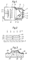
- One example of such ion-beam etching equipment which is suitable for use in methods in accordance with the present invention is shown in a very schematic and basic form in Figure 1.
- the equipment is in the form of a double vacuum chamber 1,2 which is evacuated via a pumping port 3 by for example a diffusion pump.
- the body 10 which is to be etched by an ion beam 11 is mounted on an electrically-isolated target holder 4 in the work chamber 2.
- This target holder 4 may be for example water-cooled and/or rotatable in the chamber 2 so that the temperature of the body 10 and angle of incidence of the ion beam 11 can be controlled as desired during ion bombardment.
- the ions forming the beam 11 are generated in the source chamber 1 using a low-pressure gas discharge between a heated cathode 5 and a surrounding cylindrical anode 6.
- the gas to be ionized (usually argon) is introduced into the chamber 2 via a variable leak valve 7 at a typical pressure of for example 10 -3 torr to 5 x 10 -4 torr.
- the gas is ionized by electrons 15 from the cathode 5 which are accelerated in the radial electric field (for example 30 to 60 eV) between the cathode 5 and anode 6.
- a solenoid magnet 8 is present around the chamber 1 so that the electrons 15 move in cycloidal trajectories in a magnetic field thereby enhancing the ionization efficiency at low pressures.
- the source chamber 1 (and in particular the cylindrical anode 6) is held at a moderately high positive potential (which is less than 10 kV) to accelerate, extract and focus the ions from the chamber 1 as a beam 11, via a set of two or more optically-aligned acceleration grids 12 and 13.
- the first grid 12 which is at the anode potential forms a permeable wall of the discharge chamber 1, while the second grid 13 which is at a negative potential (for example -250V) prevents electrons travelling from the chamber 1 through the grid system 12, 13 and provides the accelerating and focussing voltage for the ion beam 11.
- a filament 14 located beyond the grid system 12, 13 and immersed in the ion beam 11 emits electrons into the beam 11 to neutralize the positive space charge of the beam 11 so reducing its electrostatic divergence and substantially balancing the surface charge on the body 10 bombarded by the beam 11.
- the body 10 is thus etched in a substantially field-free and plasma-free environment.
- a movable shutter 18 is present in the chamber 2 and can be moved into the path between the chamber 1 and the target holder 4 to interrupt the beam 11 so permitting easy control of the bombardment time. This is particularly important for short bombardment times.
- Such ion-beam etching equipment may use voltages of up to 5kV (depending on the type of equipment) to produce argon ion beams 11 of up to 5 keV energy.
- ion beam currents of up to 1.5 milliAmps/cm 2 may be used, corresponding to approximately 10 16 ions per cm per sec.
- Such equipment operates at significantly lower voltages than ion-implantation machines (typically above 100 keV) and are considerably less complicated, easier to maintain fully operational, easier to house, and cheaper to purchase.
- Figure 2 illustrates the use of such ion-beam etching equipment in the manufacture of an infra-red radiation detector device in accordance with the present invention.
- a body 10 of cadmium mercury telluride mounted on the target holder 4 is bombarded by the ion beam 11 in the target chamber 2 of such ion-beam etching equipment.
- the body 10 will often be present on a supporting substrate of the device (for example of sapphire ),so that this substrate rather than the body 10 will directly contact the target holder 4.
- the body 10 as originally provided has the conductivity characteristics of p-type material at least at the operating temperature of the device.
- the operating temperature is usually 77 0 K, whereas the operating temperature for detectors in the 3 to 5 micrometre band may even be as high as room temperature.
- the original upper surface of the original p-type body 10 is indicated by the broken line 20 in Figure 2.
- the whole upper surface 20 of the body 10 is bombarded with the ions 11 in such a way as to etch away a part 21 of the body 10 at the whole surface 20 and to convert an underlying part 22 of the body 10 into material having conductivity characteristics of the n-type at the operating temperature of the device.
- the dose, energy and mass of the bombarding ions of the beam 11 are chosen such that adjacent the bombarded surface a sufficient excess concentration of mercury is produced from the etched-away part 21 as to act as a donor-dopant diffusion source for overdoping the acceptor-levels in the adjacent part 22 over a depth (d) which is greater than twice the penetration depth of the ions in the body 10.
- the ion bombardment energy is considerably less than 30 keV.
- a total argon ion dose of more than 10 15 ions per cm is used.
- the Applicants started with a p-type cadmium mercury telluride body 10 having an acceptor concentration of 10 16 cm -3 3 2 -1 -1 and a mobility of 2 x 10 cm V sec .
- This body 10 was bombarded in a VEECO "Microetch" system, with a beam current of 600 microAmps per cm 2 of 500eV neutralised argon ions. This beam current corresponds to an ion dose per minute of approximately 2 x 10 17 ions per cm 2 .
- the target-holder 4 was water-cooled at a temperature of approximately 10°C. By bombardment in this way the p-type material was converted to n-type at a rate given by the graph of Figure 4.
- t is the bombardment time in minutes whereas d is the thickness of the resulting n-type part 22 (i.e. not including the thickness of the part 21 which was etched away).
- d is the thickness of the resulting n-type part 22 (i.e. not including the thickness of the part 21 which was etched away).
- the conversion depth d in this example was found to be approximately proportional to t 0.85 .
- a two-minute bombardment produced a 10 micrometre thick n-type layer 22, whereas a 60 minute bombardment produced an n-type layer 22 of just over 200 micrometres thickness.
- the technique can be used to convert a p-type cadmium mercury telluride body into n-type material over its whole thickness.
- the thickness of the body part 21 etched under those conditions is approximately 0.5 micrometres in 2 minutes and approximately 15 micrometres in 60 minutes.
- the penetration depth of the 500 eV argon ions in the body 10 is very small (approximately 0.2 micrometre).
- the resulting average donor concentration in the n-type layer 22 was measured as 1.4 x 10 15 cm and the mobility was 9.6 x 10 4 cm 2 V sec -1 .
- a lower ion energy is used (compared with implantation) so that when a significant part 21 of the body 10 is etched-away some of the mercury from the etched-away part 21 is driven into the body 10 as dopant interstitials in the crystal lattice.
- the surprisingly large conversion depths obtained indicate that this interstitial mercury is formed in a sufficiently large excess concentration as to move further into the body 10 by a diffusion process during the ion-etching. Without such diffusion the conversion depth would merely be of approximately the same order of magnitude as the penetration depth of the ions (approximately 0.2 micrometres for 500 eV argon ions) and would not increase with time in the manner found.
- the conductivity type conversion effect can be represented by the following very simplified model, assuming a linear gradient of interstitial mercury in the converted part 22 from a high concentration n 0 at the bombarded surface of part 22 to a lower concentration which occurs at the 2 -a junction 23 and which equals the acceptor level concentration p 0 in a remaining part 24 of the body 10. It should be noted that this assumption and the simplified model are not an accurate representation pf what occurs but nevertheless do offer some assistance in understanding the conversion effect which is obtained in practice.
- N is the concentration of interstitial mercury generated
- t is the bombardment and etching time
- D is the diffusion coefficient of the interstitial mercury in the cadmium mercury telluride body 10
- d is the thickness of the n-type converted part 22.
- Equation (3) represents a conversion depth (d) which is linear in time (t) and increases at a rate given by (G/p o ).
- G generation rate
- p o original acceptor doping concentration
- equation (3) gives a conversion rate which is independant of the diffusion coefficient (D) and hence of the temperature.
- the linear conversion rate of equation (3) compares reasonably well with the experimental results of Figure 4 for which the conversion depth (d) was found to increase approximately proportional to t 0.85 .
- the converted part 22 has a very high surface concentration of interstitial mercury, n , given by:
- a value for G and for n o can be derived from the Figure 4 results, using equations (3) and (4).
- p o was 10 16 acceptor levels/cm 3 , and an approximate average conversion rate of 7 x 10 -6 cm/sec can be taken from Figure 4.
- equation ( 3 ) a value of approximately 7 x 1 0 10 cm sec is obtained for G.
- equation (4) gives the following approximate values for n , (7 x 10 19 )d where d is in micrometres, or (3 x 10 20 )t where t is in minutes.
- the bombardment and etching time t is a most useful parameter to vary so as to obtain different desired conversion depths d, particularly when forming photo-voltaic p-n junctions of desired depth in the body 10 rather than converting the whole of the body 10 to n-type.
- the ion dose may also be varied by varying the ion beam current density J. As shown in Figure 5 the conversion depth d increases with increased beam current density J which is equivalent to the ion dose per unit time.
- the depth d increases from approximately 30 micrometres for 200 microAmps/cm 2 (approximately 8 x 10 16 ions/cm 2 /min) to approximately 80 micrometres for 1.4 milliAmps/cm 2 (approximately 5 x 10 17 ions/cm 2 /min), both values being obtained for the same bombardment time of 12 minutes.
- the conversion depth is of course also dependant on other parameters, for example, it decreases with increased ion size, so that when using xenon in place of argon the conversion depth (d) was found to be reduced to a fifth of the value obtained with argon ions under otherwise identical conditions.
- Changing the accelerating voltage for the ion beam 11 may be used to change the beam current available in a given ion-beam etching equipment. However it appears that if the same value of beam current can be used in each case the conversion depth obtained does not appear to be dependant (or at least not strongly dependant) on the energy of the ion beam within the energy ranges useful for ion-etching. When higher energies are used the ions penetrate so deeply in the body that no significant etching occurs at the bombarded surface, and the ion bombardment is no longer effective for conductivity type conversion in accordance with the present invention.
- Figure 3 illustrates how the body of Figure 2 may be further processed to form a photo-voltaic infra-red detector device having the p-n junction 23 as its photosensitive junction.
- the area of the junction is defined in known manner by mesa-etching using chemical etchant solutions to remove a peripheral part of the n-type region 22 over its whole thickness while masking a central part of the region 22.
- a passivating layer 26 of for example zinc sulphide is then deposited in known manner on the upper surface of the E -type region 24 and on the n-type mesa region 22.
- Metal layer electrodes 28 and 29 are provided in known manner to contact the regions 22 and 24 respectively at windows formed in the layer 26.
- the current-voltage characteristics of the p-n junction 23 of one example of a photo-voltaic infra-red detector device manufactured in this way are given in Figure 6.
- the graph of Figure 6 shows the current I in microAmps flowing through the device when a voltage V in volts is applied between its electrodes 28 and 29. The measurements were taken with the device at 77 K, which is its normal operating temperature.
- the forward characteristic in which the applied voltage forward biases the junction 23
- the reverse characteristic junction 23 reverse-biased
- This detector device was fabricated under the same ion-etching conditions as those used to obtain the results of Figure 4.
- the ion-etching time (t) was chosen to give a depth (d) of 10 micrometres from the p-n junction 23.
- the n-type mesa region 22 had a diameter of 280 micrometres.
- the device may either be used without any applied bias voltage or with a reverse bias voltage in the range corresponding to the low-current (i.e. blocking) portion of the reverse characteristic shown in Figure 6.
- the ion bombardment (and consequently the ion-etching and conversion of conductivity type) can be localised at the surface of the cadmium mercury telluride body 10.
- a masking layer 31 for example of photoresist
- the use of a photoresist layer to mask locally against ion-etching is already described in the previously mentioned patent specifications of DE 2708792, EP 0 007 667, EP 0 007 668 and EP 0 007 669.
- the masking layer 31 is removed before providing a passivating layer 26 and electrodes 28 and 29 as in the previously described example.
- the resulting photo-voltaic detector structure is illustrated in Figure 8. A plurality of such detectors can be formed in the body 10.
Landscapes
- Light Receiving Elements (AREA)
- Radiation Pyrometers (AREA)
- Measurement Of Radiation (AREA)
Applications Claiming Priority (2)
| Application Number | Priority Date | Filing Date | Title |
|---|---|---|---|
| GB8109774A GB2095898B (en) | 1981-03-27 | 1981-03-27 | Methods of manufacturing a detector device |
| GB8109774 | 1981-03-27 |
Publications (2)
| Publication Number | Publication Date |
|---|---|
| EP0062367A1 true EP0062367A1 (fr) | 1982-10-13 |
| EP0062367B1 EP0062367B1 (fr) | 1985-02-20 |
Family
ID=10520731
Family Applications (1)
| Application Number | Title | Priority Date | Filing Date |
|---|---|---|---|
| EP82200319A Expired EP0062367B1 (fr) | 1981-03-27 | 1982-03-11 | Procédé de fabrication d'un dispositif détecteur et dispositif détecteur obtenu |
Country Status (6)
| Country | Link |
|---|---|
| US (1) | US4411732A (fr) |
| EP (1) | EP0062367B1 (fr) |
| JP (1) | JPS57170577A (fr) |
| DE (1) | DE3262369D1 (fr) |
| GB (1) | GB2095898B (fr) |
| IL (1) | IL65339A0 (fr) |
Cited By (2)
| Publication number | Priority date | Publication date | Assignee | Title |
|---|---|---|---|---|
| EP0107202A1 (fr) * | 1982-10-25 | 1984-05-02 | CSELT Centro Studi e Laboratori Telecomunicazioni S.p.A. | Dispositif opto-électronique et son procédé de fabrication |
| FR2604298A1 (fr) * | 1986-09-19 | 1988-03-25 | Commissariat Energie Atomique | Procede de realisation d'une prise de contact electrique sur un substrat en hgcdte de conductivite p et application a la fabrication d'une diode n/p |
Families Citing this family (36)
| Publication number | Priority date | Publication date | Assignee | Title |
|---|---|---|---|---|
| US4559695A (en) * | 1981-03-27 | 1985-12-24 | U.S. Philips Corporation | Method of manufacturing an infrared radiation imaging device |
| DE3200853A1 (de) * | 1982-01-14 | 1983-07-21 | Licentia Patent-Verwaltungs-Gmbh, 6000 Frankfurt | Halbleiteranordnung mit einer bildaufnahmeeinheit und mit einer ausleseeinheit sowie verfahren zu ihrer herstellung |
| DE3227263C2 (de) * | 1982-07-21 | 1984-05-30 | Siemens AG, 1000 Berlin und 8000 München | Verfahren zur Herstellung einer planaren Avalanche-Fotodiode mit langwelliger Empfindlichkeitsgrenze über 1,3 μ |
| US4682022A (en) * | 1985-02-21 | 1987-07-21 | The Perkin-Elmer Corporation | Detector preamplifier for use with a MCT detector |
| US5079610A (en) * | 1985-12-05 | 1992-01-07 | Santa Barbara Research Center | Structure and method of fabricating a trapping-mode |
| US5004698A (en) * | 1985-12-05 | 1991-04-02 | Santa Barbara Research Center | Method of making photodetector with P layer covered by N layer |
| US5182217A (en) * | 1985-12-05 | 1993-01-26 | Santa Barbara Research Center | Method of fabricating a trapping-mode |
| US4639756A (en) * | 1986-05-05 | 1987-01-27 | Santa Barbara Research Center | Graded gap inversion layer photodiode array |
| US4956304A (en) * | 1988-04-07 | 1990-09-11 | Santa Barbara Research Center | Buried junction infrared photodetector process |
| US4961098A (en) * | 1989-07-03 | 1990-10-02 | Santa Barbara Research Center | Heterojunction photodiode array |
| US5049962A (en) * | 1990-03-07 | 1991-09-17 | Santa Barbara Research Center | Control of optical crosstalk between adjacent photodetecting regions |
| US5264699A (en) * | 1991-02-20 | 1993-11-23 | Amber Engineering, Inc. | Infrared detector hybrid array with improved thermal cycle reliability and method for making same |
| US5308980A (en) * | 1991-02-20 | 1994-05-03 | Amber Engineering, Inc. | Thermal mismatch accommodated infrared detector hybrid array |
| US5241196A (en) * | 1991-10-15 | 1993-08-31 | Santa Barbara Research Center | Photoresponsive device including composition grading and recessed contacts for trapping minority carriers |
| GB9204078D0 (en) * | 1992-02-26 | 1992-04-08 | Philips Electronics Uk Ltd | Infrared detector manufacture |
| US5300777A (en) * | 1992-03-26 | 1994-04-05 | Texas Instruments Incorporated | Two color infrared detector and method |
| US5436450A (en) * | 1994-01-13 | 1995-07-25 | Texas Instruments Incorporated | Infrared detector local biasing structure and method |
| US5426304A (en) * | 1994-01-13 | 1995-06-20 | Texas Instruments Incorporated | Infrared detector thermal isolation structure and method |
| US5485010A (en) * | 1994-01-13 | 1996-01-16 | Texas Instruments Incorporated | Thermal isolation structure for hybrid thermal imaging system |
| US5559332A (en) * | 1994-11-04 | 1996-09-24 | Texas Instruments Incorporated | Thermal detector and method |
| US5536680A (en) * | 1995-05-08 | 1996-07-16 | Texas Instruments Incorporated | Self-aligned bump bond infrared focal plane array architecture |
| US5708269A (en) * | 1995-08-15 | 1998-01-13 | Raytheon Ti Systems, Inc. | Thermal detector and method |
| US6249374B1 (en) | 1996-03-04 | 2001-06-19 | Raytheon Company | Wide field of view infrared zoom lens assembly having a constant F/number |
| US5852516A (en) * | 1996-03-04 | 1998-12-22 | Raytheon Ti Systems, Inc. | Dual purpose infrared lens assembly using diffractive optics |
| US6018414A (en) * | 1996-03-04 | 2000-01-25 | Raytheon Company | Dual band infrared lens assembly using diffractive optics |
| US5796514A (en) * | 1996-03-04 | 1998-08-18 | Raytheon Ti Systems, Inc. | Infrared zoom lens assembly having a variable F/number |
| US6281035B1 (en) * | 1997-09-25 | 2001-08-28 | Midwest Research Institute | Ion-beam treatment to prepare surfaces of p-CdTe films |
| US6458254B2 (en) * | 1997-09-25 | 2002-10-01 | Midwest Research Institute | Plasma & reactive ion etching to prepare ohmic contacts |
| US6486476B1 (en) * | 1998-12-22 | 2002-11-26 | Hitachi, Ltd. | Semiconductor radiation detector and manufacture thereof |
| DE10024473B4 (de) | 2000-05-18 | 2007-04-19 | Vishay Semiconductor Gmbh | Optischer Empfänger |
| US20070227578A1 (en) * | 2006-03-31 | 2007-10-04 | Applied Materials, Inc. | Method for patterning a photovoltaic device comprising CIGS material using an etch process |
| US7547570B2 (en) * | 2006-03-31 | 2009-06-16 | Applied Materials, Inc. | Method for forming thin film photovoltaic interconnects using self-aligned process |
| US7718347B2 (en) * | 2006-03-31 | 2010-05-18 | Applied Materials, Inc. | Method for making an improved thin film solar cell interconnect using etch and deposition process |
| US20080311762A1 (en) * | 2007-06-18 | 2008-12-18 | Mark Doczy | Semiconductor device surface roughness reduction |
| RU2609222C1 (ru) * | 2015-11-20 | 2017-01-31 | Федеральное государственное автономное образовательное учреждение высшего образования "Национальный исследовательский Томский государственный университет" (ТГУ, НИ ТГУ) | СПОСОБ ОПРЕДЕЛЕНИЯ КОНЦЕНТРАЦИИ ДОНОРНОГО ФОНА В СТРУКТУРАХ CdxHg1-xTe |
| US11251075B2 (en) * | 2018-08-06 | 2022-02-15 | Mattson Technology, Inc. | Systems and methods for workpiece processing using neutral atom beams |
Citations (2)
| Publication number | Priority date | Publication date | Assignee | Title |
|---|---|---|---|---|
| US3562022A (en) * | 1967-12-26 | 1971-02-09 | Hughes Aircraft Co | Method of doping semiconductor bodies by indirection implantation |
| EP0007667A1 (fr) * | 1978-07-31 | 1980-02-06 | Philips Electronics Uk Limited | Eléments détecteurs infra-rouge et leur fabrication |
Family Cites Families (3)
| Publication number | Priority date | Publication date | Assignee | Title |
|---|---|---|---|---|
| DE2708792C3 (de) * | 1977-03-01 | 1980-07-10 | Licentia Patent-Verwaltungs-Gmbh, 6000 Frankfurt | Verwendung des Ionenätzverf ahrens zum Strukturieren von Halbleiterschichten und Ionenätzverfahren für diese Verwendung |
| GB2027556B (en) * | 1978-07-31 | 1983-01-19 | Philips Electronic Associated | Manufacturing infra-red detectors |
| GB2027985B (en) * | 1978-07-31 | 1983-01-19 | Philips Electronic Associated | Infra-red detectors |
-
1981
- 1981-03-27 GB GB8109774A patent/GB2095898B/en not_active Expired
-
1982
- 1982-03-03 US US06/355,440 patent/US4411732A/en not_active Expired - Lifetime
- 1982-03-11 EP EP82200319A patent/EP0062367B1/fr not_active Expired
- 1982-03-11 DE DE8282200319T patent/DE3262369D1/de not_active Expired
- 1982-03-24 IL IL65339A patent/IL65339A0/xx not_active IP Right Cessation
- 1982-03-27 JP JP57048194A patent/JPS57170577A/ja active Granted
Patent Citations (2)
| Publication number | Priority date | Publication date | Assignee | Title |
|---|---|---|---|---|
| US3562022A (en) * | 1967-12-26 | 1971-02-09 | Hughes Aircraft Co | Method of doping semiconductor bodies by indirection implantation |
| EP0007667A1 (fr) * | 1978-07-31 | 1980-02-06 | Philips Electronics Uk Limited | Eléments détecteurs infra-rouge et leur fabrication |
Non-Patent Citations (1)
| Title |
|---|
| IEEE TRANSACTIONS ON ELECTRON DEVICES Vol. ED-27, No. 1, January 1980, New York, KOLODNY et al.: " Properties of Ion-Implanted Junctions in Mercury-Cadmium-Telluride" pages 37 to 43 * |
Cited By (4)
| Publication number | Priority date | Publication date | Assignee | Title |
|---|---|---|---|---|
| EP0107202A1 (fr) * | 1982-10-25 | 1984-05-02 | CSELT Centro Studi e Laboratori Telecomunicazioni S.p.A. | Dispositif opto-électronique et son procédé de fabrication |
| FR2604298A1 (fr) * | 1986-09-19 | 1988-03-25 | Commissariat Energie Atomique | Procede de realisation d'une prise de contact electrique sur un substrat en hgcdte de conductivite p et application a la fabrication d'une diode n/p |
| EP0262030A1 (fr) * | 1986-09-19 | 1988-03-30 | Commissariat A L'energie Atomique | Procédé de réalisation d'une prise de contact électrique sur un substrat en HgCdTe de conductivité P et application à la fabrication d'une diode N/P |
| US4766084A (en) * | 1986-09-19 | 1988-08-23 | Commissariat A L'energie Atomique | Process for the production of an electric contact on a HgCdTe substrate with a P conductivity and application to the production of an N/P diode |
Also Published As
| Publication number | Publication date |
|---|---|
| US4411732A (en) | 1983-10-25 |
| GB2095898B (en) | 1985-01-09 |
| GB2095898A (en) | 1982-10-06 |
| EP0062367B1 (fr) | 1985-02-20 |
| JPS6244868B2 (fr) | 1987-09-22 |
| DE3262369D1 (en) | 1985-03-28 |
| JPS57170577A (en) | 1982-10-20 |
| IL65339A0 (en) | 1982-05-31 |
Similar Documents
| Publication | Publication Date | Title |
|---|---|---|
| EP0062367B1 (fr) | Procédé de fabrication d'un dispositif détecteur et dispositif détecteur obtenu | |
| US3551213A (en) | Geometrically selective ion bombardment by means of the photoelectric effect | |
| US3496029A (en) | Process of doping semiconductor with analyzing magnet | |
| US6013332A (en) | Boron doping by decaborane | |
| KR100351489B1 (ko) | 반도체기판내에회로및매립절연층을형성하는방법 | |
| EP0132015B1 (fr) | Dispositif d'usinage par faisceau d'ions | |
| GB1336845A (en) | Methods of manufacturing a semiconductor device | |
| US3562022A (en) | Method of doping semiconductor bodies by indirection implantation | |
| US4104085A (en) | Method of manufacturing a semiconductor device by implanting ions through bevelled oxide layer in single masking step | |
| US4096622A (en) | Ion implanted Schottky barrier diode | |
| US5196706A (en) | Extractor and deceleration lens for ion beam deposition apparatus | |
| US3431150A (en) | Process for implanting grids in semiconductor devices | |
| US4151011A (en) | Process of producing semiconductor thermally sensitive switching element by selective implantation of inert ions in thyristor structure | |
| US4851691A (en) | Method for photoresist pretreatment prior to charged particle beam processing | |
| Wotherspoon | Methods of manufacturing a detector device | |
| US3983574A (en) | Semiconductor devices having surface state control | |
| EP0001139B1 (fr) | Diode à avalanche sensible aux rayonnements et son procédé de fabrication | |
| US3536547A (en) | Plasma deposition of oxide coatings on silicon and electron bombardment of portions thereof to be etched selectively | |
| US3956025A (en) | Semiconductor devices having surface state control and method of manufacture | |
| US4663830A (en) | Forming deep buried grids of implanted zones being vertically and laterally offset by mask MEV implant | |
| US3620851A (en) | Method for making a buried layer semiconductor device | |
| US3591424A (en) | P-n junction photoemitters | |
| US6191012B1 (en) | Method for forming a shallow junction in a semiconductor device using antimony dimer | |
| US4003759A (en) | Ion implantation of gold in mercury cadmium telluride | |
| JPH03134947A (ja) | イオン注入装置および電荷中和器 |
Legal Events
| Date | Code | Title | Description |
|---|---|---|---|
| PUAI | Public reference made under article 153(3) epc to a published international application that has entered the european phase |
Free format text: ORIGINAL CODE: 0009012 |
|
| 17P | Request for examination filed |
Effective date: 19820311 |
|
| AK | Designated contracting states |
Designated state(s): DE FR GB IT |
|
| ITF | It: translation for a ep patent filed | ||
| GRAA | (expected) grant |
Free format text: ORIGINAL CODE: 0009210 |
|
| AK | Designated contracting states |
Designated state(s): DE FR GB IT |
|
| REF | Corresponds to: |
Ref document number: 3262369 Country of ref document: DE Date of ref document: 19850328 |
|
| ET | Fr: translation filed | ||
| PLBE | No opposition filed within time limit |
Free format text: ORIGINAL CODE: 0009261 |
|
| STAA | Information on the status of an ep patent application or granted ep patent |
Free format text: STATUS: NO OPPOSITION FILED WITHIN TIME LIMIT |
|
| 26N | No opposition filed | ||
| REG | Reference to a national code |
Ref country code: GB Ref legal event code: 732 |
|
| ITTA | It: last paid annual fee | ||
| REG | Reference to a national code |
Ref country code: FR Ref legal event code: TP |
|
| REG | Reference to a national code |
Ref country code: GB Ref legal event code: 732E |
|
| PGFP | Annual fee paid to national office [announced via postgrant information from national office to epo] |
Ref country code: FR Payment date: 20010312 Year of fee payment: 20 |
|
| PGFP | Annual fee paid to national office [announced via postgrant information from national office to epo] |
Ref country code: GB Payment date: 20010319 Year of fee payment: 20 |
|
| PGFP | Annual fee paid to national office [announced via postgrant information from national office to epo] |
Ref country code: DE Payment date: 20010321 Year of fee payment: 20 |
|
| REG | Reference to a national code |
Ref country code: GB Ref legal event code: IF02 |
|
| PG25 | Lapsed in a contracting state [announced via postgrant information from national office to epo] |
Ref country code: GB Free format text: LAPSE BECAUSE OF EXPIRATION OF PROTECTION Effective date: 20020310 |
|
| REG | Reference to a national code |
Ref country code: GB Ref legal event code: PE20 Effective date: 20020310 |