EP0062411B1 - Verfahren und Gerät zur Münzprüfung - Google Patents
Verfahren und Gerät zur Münzprüfung Download PDFInfo
- Publication number
- EP0062411B1 EP0062411B1 EP82301161A EP82301161A EP0062411B1 EP 0062411 B1 EP0062411 B1 EP 0062411B1 EP 82301161 A EP82301161 A EP 82301161A EP 82301161 A EP82301161 A EP 82301161A EP 0062411 B1 EP0062411 B1 EP 0062411B1
- Authority
- EP
- European Patent Office
- Prior art keywords
- coin
- phase shift
- feedback loop
- feedback
- network
- Prior art date
- Legal status (The legal status is an assumption and is not a legal conclusion. Google has not performed a legal analysis and makes no representation as to the accuracy of the status listed.)
- Expired
Links
- 238000010200 validation analysis Methods 0.000 title claims abstract description 26
- 238000000034 method Methods 0.000 title claims abstract description 8
- 230000010363 phase shift Effects 0.000 claims abstract description 57
- 230000000694 effects Effects 0.000 claims abstract description 5
- 238000012544 monitoring process Methods 0.000 claims description 16
- 230000010355 oscillation Effects 0.000 claims description 10
- 230000001419 dependent effect Effects 0.000 claims description 3
- 239000007787 solid Substances 0.000 claims description 3
- 230000007246 mechanism Effects 0.000 abstract description 4
- 230000003993 interaction Effects 0.000 abstract description 3
- 230000015654 memory Effects 0.000 description 17
- 230000008859 change Effects 0.000 description 5
- 239000003990 capacitor Substances 0.000 description 3
- 239000013078 crystal Substances 0.000 description 3
- 238000010586 diagram Methods 0.000 description 3
- 239000003985 ceramic capacitor Substances 0.000 description 2
- 230000006870 function Effects 0.000 description 2
- 238000005259 measurement Methods 0.000 description 2
- 230000000903 blocking effect Effects 0.000 description 1
- 230000000977 initiatory effect Effects 0.000 description 1
- 230000008569 process Effects 0.000 description 1
Images


Classifications
-
- G—PHYSICS
- G07—CHECKING-DEVICES
- G07D—HANDLING OF COINS OR VALUABLE PAPERS, e.g. TESTING, SORTING BY DENOMINATIONS, COUNTING, DISPENSING, CHANGING OR DEPOSITING
- G07D5/00—Testing specially adapted to determine the identity or genuineness of coins, e.g. for segregating coins which are unacceptable or alien to a currency
- G07D5/08—Testing the magnetic or electric properties
Definitions
- Coin validation apparatus may be associated with a coin freed mechanism on a variety of coin receiving machines such as coin box telephones or vending machines or form part of a coin sorting apparatus to check that coins are valid coins and not counterfeit.
- coin validation apparatus There are many different types of coin validation apparatus in use, but recently, with the introduction of modern electronic devices to control the operation of coin receiving machines and sorting apparatus, it has become particularly convenient to use the interaction between a coin and an alternating magnetic field to gauge various parameters of the coin thereby to determine if the coin is valid.
- coin validation apparatus comprises an electrical coil, a feedback oscillator having the electrical coil in its feedback loop, frequency monitoring means for monitoring the frequency of the feedback oscillator and for producing an output signal indicative of its frequency, and means to compare signals with reference values to determine if the coin is valid.
- the frequency of the feedback oscillator is also monitored when a phase shift or time delay network is included in its feedback loop, two parameter signals characteristic of the effect of the coin on both the inductance and the loss factor of the coil are derived from the monitored frequencies and the two parameter signals are compared with reference values to determine if the coil is valid.
- the oscillation frequency of a tuned circuit feedback oscillator is dependent upon the inductance and loss factor of components within its feedback loop.
- the presence of a coin adjacent an electrical coil affects the inductance and loss factor of that electrical coil.
- information is derived with regard to the inductance and loss factor of components within its feedback loop which, to some extent, depends upon the nature of the coin.
- a phase shift or time delay network is selectively connected into the feedback loop of the feedback oscillator to introduce a particular known change in the characteristics of the feedback loop which results in a change in the frequency of the feedback oscillator, making it differ by an amount depending upon the coil loss resistance.
- the resonant frequency of the oscillator when the phase shift is not connected in the feedback loop is representative of the inductance of the coil and the change in frequency which occurs when the phase shift or time delay network is included in the feedback loop is representative of the loss factor of the coil.
- the presence of a coil adjacent the coil has an influence on both the inductance and loss factor of the coil and consequently the monitored frequencies of the oscillator give an indication of the properties and characteristics of the coin.
- such a coil validation apparatus also includes means to hold a coin at a fixed reference position adjacent the electrical coil, a phase shift or time delay network switchable into and out of its feedback loop, and means responsive to the output signal of the frequency monitoring means both when the phase shift or time delay network is switched into and out of the feedback loop for producing two parameter signals characteristic of the effect of the coin on both the inductance and loss factor of the coil, the means to compare comparing the two parameter signals with reference values to determine if the coin is valid and to output a coin validation signal when both parameter signals correspond to reference values.
- the frequency monitoring means, the means responsive to the output signal of the frequency monitoring means for producing the two parameter signals and the means to compare the two parameter signals with reference values may comprise a programmed microprocessor which is programmed to compare the output signal produced when the phase shift or time delay network is switched into the feedback loop of the feedback oscillator with the output signal produced when the phase shift or time delay network is switched out of the feedback loop to produce a first parameter signal and to produce a second parameter signal dependent upon the output signal produced when the phase shift or time delay network is switched out of the feedback loop.
- the second parameter signal may be the output signal produced when the phase shift of the delay network is switched out of the feedback loop or this output signal may be operated on by a fixed operator such as a constant division or subtraction.
- the means responsive to the output signal of the frequency monitoring means for producing the two parameter signals may comprise first storage means for storing the output signal produced when the time delay or phase shift network is switched out of the feedback loop, first comparison means for comparing the output signals produced when the phase shift or time delay network is switched into the feedback loop with that produced when the phase shift or time delay network is switched out of the feedback loop to produce a first parameter signal, second storage means for storing at least two reference values, and second comparison means to compare the first parameter signal and the content of the first storage means which forms the second parameter signal, with the reference values stored in the second storage means to produce a coin validation signal when both coin parameter signals correspond to the stored reference values.
- this means may be implemented either by a dedicated microprocessor arranged to perform this particular sequence of operations or by a hard wired logic circuit.
- phase shift network When a phase shift network is included it may be arranged to produce a constant fixed phase shift irrespective of the resonant frequency of the oscillator and this fixed phase shift is preferably a phase shift of about 45°.
- time delay network When a time delay network is included it may be arranged to introduce a fixed time delay and in this case the resulting phase shift that is introduced by the time delay network varies with the resonant frequency of the oscillation.
- the frequency of the oscillation depends to some extent upon the nature of the coin, and the frequency change brought about by the particular phase shift introduced by the phase shift or time delay network thus also depends to some extent upon the nature of the coin. Thus, even if the phase shift varies, the values of the two parameter signals are repeatable for coins of a particular denomination.
- the phase shift network includes an operational amplifier having a parallel connected capacitive and resistive feedback network and an input resistor connected between the inverting input of the operational amplifier and ground.
- This integrating network provides a phase shift that varies to a small extent with the frequency of oscillation of the oscillator.
- a solid state switch is provided in parallel with the resistive capacitive feedback network of the operational amplifier to short out the parallel capacitive and resistive feedback network of the operational amplifier when the phase shift network is to be switched out of the feedback loop of the feedback oscillator.
- This solid state switch is preferably formed by a transistor.
- the coil is formed in two parts connected in series.
- the fixed reference position of the coin with respect to the coils is with the coin located in between the two parts of the coil, and located against a stop. This ensures that the lines of force of the magnetic field induced by the coil are substantially normal to the face of the coin and this enables reliable and consistent measurements to be taken of the influence of the coin on the coil.
- the switching of the phase shift network into and out of the feedback loop of the feedback oscillator is preferably controlled by signals taken from the microprocessor.
- the phase shift network under the control of a free running multi-vibrator.
- the frequency monitoring means preferably includes a counter arranged to count the number of the oscillations of the feedback oscillator that occur within a preset time interval.
- the preset time interval may correspond to the time interval during which the phase shift network is connected into the feedback loop of the oscillator.
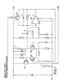
- the coin validation apparatus also includes the coin runway described in our Published European Patent Application No. 0 040 019 which is incorporated herein by reference. It is the arrangement of this pivoting runway which determines the fixed reference position of the coin with reference to an electrical coil 1.
- the coil 1 is formed in two halves connected in series with one half on one side of the coin runway and the other half on the other side of the runway.
- the coil 1 together with a pair of ceramic capacitors 2 and 3 connected in parallel form a resonant tank circuit connected to the collector of one of a long tailed pair formed by transistors TR2 and TR3.
- the capacitors 2 and 3 are NPO type ceramic capacitors which have a very small temperature coefficient of not greater than 30 ppm/°C and thus the temperature stability of the resonant tank circuit is high.
- the long tailed pair formed by transistors TR2 and TR3 together with the tank circuit comprise a feedback oscillator, having a feedback loop joining the collector of transistor TR3 to the base of transistor TR2.
- the feedback loop includes a phase shift network including a DC blocking capacitor 4, an operational amplifier 5 which is a model No. ICL 7611 manufactured by INTERSIL and which has a resistance 6 and a capacitance 7 connected in parallel in a feedback loop across the operational amplifier 5.
- a resistor 8 is connected between the inverting input of the operational amplifier 4 and a.c. ground.
- a transistor TR4 acting as a switch is also connected in parallel with the resistance 6 and capacitance 7 across the feedback path of the operational amplifier 5.
- the resistance 6 and capacitance 7 are switched out of the feedback path of the operational amplifier 5 since a direct connection is established, short circuiting the capacitance 7 and the resistor 6.
- the oscillating output from the feedback oscillator is taken from the collector of transistor TR2 via a buffer transistor TR1.
- the part shown in Figure 1 corresponds to the blocks contained in the chain dotted box shown in Figure 2.
- the apparatus also includes a crystal oscillator 9 having its output fed to a divider unit 10, a microprocessor 11 and memories 12 and 13.
- Memory 12 is a read only memory which stores the program which controls the operation of the microprocessor 11.
- Memory 13 is a memory storing the reference values for coins that are acceptable and this may be a random access memory or a programmable read only memory.
- the crystal oscillator 9 together with the divider 10 provides the clocking and timing signals for the entire apparatus.
- the microprocessor controls via an output port 14 the transistor TR4 which switches the phase shift network into and out of the feedback loop of the oscillator.
- the microprocessor 11 includes a counter and various other internal memories. Typically the microprocessor 11 is formed by model No. CDP 1802E manufactured by RCA. There are further inputs into the microprocessor 11 which are now shown in Figure 2 but which come from the "on hook" contacts of the telephone and so provide an indication when the handset of the telephone is lifted and an input from a simple coin detector circuit including for example a simple light emitting diode and photodetector located adjacent the coin runway, the coin detecting circuit providing an indication when a coin is introduced into the coin freed mechanism.
- a simple coin detector circuit including for example a simple light emitting diode and photodetector located adjacent the coin runway, the coin detecting circuit providing an indication when a coin is introduced into the coin freed mechanism.
- the apparatus When the handset is in place on the receiver of the telephone the apparatus is isolated from the power supply and has a zero power consumption. However, the voltage appearing across the telephone line is used to charge up a battery forming part of the apparatus to provide a power supply for the circuits when they are in operation. As the handset of the telephone is lifted from its cradle the "on hook" contacts of the telephone are arranged to connect the power supply to the circuits forming the coin validation apparatus. As the microprocessor 11 is being powered up, the first operation that takes place is the initiation of a 200 millisecond delay to allow the entire circuits to power up correctly.
- an output signal is obtained from the coin detector and fed to the microprocessor 11. This initiates a delay of 1/3 of a second to allow sufficient time for the coin to come to rest in its fixed stable position against a stop formed by part of the coin runway so that the coin is in a fixed position between the two halves of the coil 1. Upon expiry of this 1/3 of a second delay the microprocessor 11 then starts its validation function and the oscillator starts with the transistor TR4 conducting and the phase shift network formed by the capacitor 6 and resistor 7 switched out of the feedback loop of the oscillator.
- the counter in the microprocessor counts the number of changes in polarity from plus to minus that occur within a 3.75 millisecond period and stores the result in an internal memory of the microprocessor.
- the transistor TR4 is then switched off and the number of changes in polarity of the output of the oscillator from plus to minus that occur in a 3.75 millisecond period is again counted and, at the end of this 3.75 millisecond period the count is stored in another memory of the microprocessor 11.
- These two processes may be repeated for, for example, five to fifteen times with the results stored in a running total store to refine the measurement of the frequencies of the oscillator.
- the outputs from any such running total stores may be divided before being handled so that the number handling capacity of the microprocessor 11 is not exceeded. The difference between these two counts is derived and stored in a further internal memory.
- the information stored in this further internal memory represents the difference between the frequency of the oscillator with the phase shift network switched into and out of the feedback loop when a coin is present in the coil 1.
- This difference in frequency gives an indication of the characteristics or nature of the coin in so far as it affects the loss resistance of the coil 1.
- the difference frequency provides the first parameter signal.
- the count stored in the memory and corresponding to that recorded when the coin is present in the coil 1 and the phase shift network is switched out of the feedback loop of the oscillator represents the second parameter signal that gives an indication of the characteristics or nature of the coin in so far as it affects the inductance of the coil 1.
- the number of changes in polarity that occur within the period of 3.75 milliseconds may be subjected to a constant mathematical operation such as a division or a subtraction to convert it into the second parameter signal. This is especially useful if the number of changes in polarity is high and so would, for example, exceed the number handling capacity of the microprocessor 11 or would necessitate a more powerful microprocessor.
- the first and second parameter signals are both then compared with various acceptable values programmed into the memory 13 and if the two signals are characteristic of a valid coin an output signal is given from the microprocessor 11 firstly indicating that the coil is a valid coin and secondly indicating the denomination of that valid coin.
- the memory 13 has a number of stored values and each of the values characteristic of the coin is compared with the stored values to make sure that each value is both greater than one of the stored values and less than the next of the stored values to provide an acceptance window to allow for a slight spread in the properties of the characteristics of coins that are acceptable.
- the memory 13 is loaded with the values of acceptable 2p, 5p, 10p and 50p coins.
- the acceptance or rejection signal is used to control the coin runway to release the coin from its position against the stop to accommodate the coin in an acceptance channel for subsequent transfer to a coin box, or to accommodate the coin in a rejection channel for return to the user.
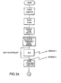
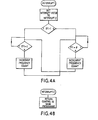
- Figures 3A, B and C together illustrate the decision flow chart of the main program stored in the read only memory 12 and Figures 4A and B illustrate the two interrupt sub-routines that join the part of the main program illustrated in Figures 3A and 3B as interrupts 1 and 2.
- the apparatus that has been described operates on current British currency and checks for the presence of four different denominations of coin.
- the program can be modified readily to enable it to check for the presence of less or more than four different denominations of coin.
- the reference values which are stored in the read only memory 13 and which define the acceptance values for valid coins are arranged to suit those of the coins of the particular currency to be validated.
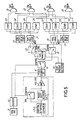
- FIG. 5 A second example of the apparatus is shown in Figure 5.
- This example is a hard wired version of the coin validator circuit which basically performs the same functions as the circuit including the microprocessor described above. As far as possible the same reference numbers have been used in Figure 5 as those used in the first example.
- the power supply to the circuit is again connected upon lifting of the handset and closure of the "on hook" contacts of the telephone.
- the number of polarity reversals of the output of the oscillator in a unit time, for example 5 milliseconds, is computed by a counter 15 and fed through a control switch 16 into a subtractor 17 or through a further control switch 18 towards a frequency store 19.
- the control switch 16 is under the control of an output from the crystal oscillator 9 and divider 10 which also controls the operation of the switching transistor TR4 which switches the phase shift network into and out of the feedback loop.
- the count from the counter 15 is fed into the frequency store 19.
- the count from in the frequency counter 15 is fed into the subtractor 17.
- the coin present detector 20 When a coin is present in the coin runway the coin present detector 20 sends a reset pulse to the frequency store 19 and a difference frequency store 21 and also operates control switches 18 and 22 so that they connect with the frequency store 19 and the difference frequency store 21 respectively.
- the count accumulated in the frequency counter 15 when the phase shift network is switched out of the feedback loop is fed to the frequency store 19 via control switches 16 and 18.
- the count accumulated in the frequency counter 15 is fed to the subtractor 17 where it is subtracted from the count in the frequency store 19 and the difference between these two values is then fed into the difference frequency store 21.
- the difference value stored in the store 21 is the first parameter signal and thus corresponds to the change in frequency of the oscillation caused by introducing the phase shift network into the feedback loop when the coin is present; and the value stored in the store 19 is the second parameter signal which corresponds to the frequency of the oscillator when the phase shift network is switched out of the feedback loop and the coin is present.
- the values stored in the stores 19 and 21 are compared with the reference values stored in the coin accept value store 15 (which for convenience is shown as two separate units) in comparators 23 to 30.
- the outputs of the comparators 23 and 27; 24 and 28; 25 and 29; and 26 and 30 are gated together by AND gates 31 and 34 respectively. If an output appears at the output of any one of the gates 31 to 34 this output indicates that the signals in the stores 19 and 21 both correspond to acceptable values for a coin of a particular denomination and indicate that the coin being examined is a valid coin of a particular denomination.
- This acceptance signal, or the failure of an acceptance signal within a preset time causes the coin to be released and taken into an acceptance channel for subsequent transfer to a coin receiving box, or rejection and return.
Landscapes
- Physics & Mathematics (AREA)
- General Physics & Mathematics (AREA)
- Pinball Game Machines (AREA)
- Testing Of Coins (AREA)
- Slot Machines And Peripheral Devices (AREA)
- Feeding, Discharge, Calcimining, Fusing, And Gas-Generation Devices (AREA)
Claims (11)
Priority Applications (1)
| Application Number | Priority Date | Filing Date | Title |
|---|---|---|---|
| AT82301161T ATE21784T1 (de) | 1981-03-19 | 1982-03-08 | Verfahren und geraet zur muenzpruefung. |
Applications Claiming Priority (2)
| Application Number | Priority Date | Filing Date | Title |
|---|---|---|---|
| GB8108625 | 1981-03-19 | ||
| GB8108625 | 1981-03-19 |
Publications (3)
| Publication Number | Publication Date |
|---|---|
| EP0062411A2 EP0062411A2 (de) | 1982-10-13 |
| EP0062411A3 EP0062411A3 (en) | 1983-12-07 |
| EP0062411B1 true EP0062411B1 (de) | 1986-08-27 |
Family
ID=10520503
Family Applications (1)
| Application Number | Title | Priority Date | Filing Date |
|---|---|---|---|
| EP82301161A Expired EP0062411B1 (de) | 1981-03-19 | 1982-03-08 | Verfahren und Gerät zur Münzprüfung |
Country Status (9)
| Country | Link |
|---|---|
| US (1) | US4460080A (de) |
| EP (1) | EP0062411B1 (de) |
| JP (1) | JPS57193884A (de) |
| AT (1) | ATE21784T1 (de) |
| AU (1) | AU543949B2 (de) |
| DE (1) | DE3272807D1 (de) |
| HK (1) | HK94987A (de) |
| SG (1) | SG44987G (de) |
| ZA (1) | ZA821411B (de) |
Families Citing this family (63)
| Publication number | Priority date | Publication date | Assignee | Title |
|---|---|---|---|---|
| DE3172063D1 (en) * | 1980-12-05 | 1985-10-03 | Autelca Ag | Circuitry for a coin tester |
| US5222076A (en) * | 1981-04-15 | 1993-06-22 | Ng William K Y | Data communication apparatus and method with low power standby mode |
| GB8303587D0 (en) * | 1983-02-09 | 1983-03-16 | Chapman Cash Processing Ltd | Coin discriminating apparatus |
| DE3486213T2 (de) * | 1983-11-04 | 1994-01-13 | Mars Inc | Münzprüfer. |
| IT1179554B (it) * | 1984-01-13 | 1987-09-16 | Urmet Spa | Gettoniera elettronica funzionante con monete di diverse pezzature e con gettoni particolarmente per uso telefonico pubblico |
| US4678994A (en) * | 1984-06-27 | 1987-07-07 | Digital Products Corporation | Methods and apparatus employing apparent resonant properties of thin conducting materials |
| GB8500220D0 (en) * | 1985-01-04 | 1985-02-13 | Coin Controls | Discriminating between metallic articles |
| US4848556A (en) * | 1985-04-08 | 1989-07-18 | Qonaar Corporation | Low power coin discrimination apparatus |
| GB8510181D0 (en) * | 1985-04-22 | 1985-05-30 | Aeronautical General Instr | Moving coin validation |
| US4705154A (en) * | 1985-05-17 | 1987-11-10 | Matsushita Electric Industrial Co. Ltd. | Coin selection apparatus |
| US4895238A (en) * | 1987-04-16 | 1990-01-23 | Pom, Incorporated | Coin discriminator for electronic parking meter |
| US4880097A (en) * | 1987-04-16 | 1989-11-14 | Pom Incorporated | Park card system for electronic parking meter |
| US4823928A (en) * | 1987-04-16 | 1989-04-25 | Pom Incorporated | Electronic parking meter system |
| US4827206A (en) * | 1987-04-16 | 1989-05-02 | Pom, Incorporated | Solar power system for electronic parking meter |
| US4967895A (en) * | 1987-04-16 | 1990-11-06 | Pom, Incorporated | Parameter control system for electronic parking meter |
| US4846332A (en) * | 1988-02-29 | 1989-07-11 | Automatic Toll Systems, Inc. | Counterfeit coin detector circuit |
| JPH01226093A (ja) * | 1988-03-07 | 1989-09-08 | Mitsubishi Heavy Ind Ltd | 硬貨判別装置 |
| US4936435A (en) * | 1988-10-11 | 1990-06-26 | Unidynamics Corporation | Coin validating apparatus and method |
| US5028870A (en) * | 1989-04-18 | 1991-07-02 | Environmental Products Corporation | Sensor system method and apparatus for discrimination of metallic objects based on a variation in self inductance |
| US5085309A (en) * | 1989-06-07 | 1992-02-04 | Adamson Phil A | Electronic coin detector |
| US5103957A (en) * | 1989-06-15 | 1992-04-14 | Am/Pm Parking Systems, Inc. | Programmable electronic parking meter with communications interface |
| US5097934A (en) * | 1990-03-09 | 1992-03-24 | Automatic Toll Systems, Inc. | Coin sensing apparatus |
| US5119916A (en) * | 1990-03-27 | 1992-06-09 | Duncan Industries Parking Control Corp. | Sensor for measuring the magnetically responsive characteristics of tokens |
| US5139128A (en) * | 1990-03-27 | 1992-08-18 | Ducan Industries Parking Control Corp. | Chute for controlling the motion of a token moving by gravity through a token-receiving device |
| GB9010507D0 (en) * | 1990-05-10 | 1990-07-04 | Mars Inc | Apparatus and method for testing coins |
| GB2253297B (en) * | 1991-02-27 | 1994-11-16 | Mars Inc | Coin validation |
| GB2254948B (en) * | 1991-04-15 | 1995-03-08 | Mars Inc | Apparatus and method for testing coins |
| US5191957A (en) * | 1991-06-28 | 1993-03-09 | Protel, Inc. | Coin discrimination method |
| US5568854A (en) * | 1991-06-28 | 1996-10-29 | Protel, Inc. | Coin discrimination method |
| US5244070A (en) * | 1992-03-04 | 1993-09-14 | Duncan Industries Parking Control Systems Corp. | Dual coil coin sensing apparatus |
| US5427220A (en) * | 1992-03-13 | 1995-06-27 | Kabushiki Kaisha Nippon Conlux | Coin processing apparatus |
| US5273151A (en) * | 1992-03-23 | 1993-12-28 | Duncan Industries Parking Control Systems Corp. | Resonant coil coin detection apparatus |
| US5360095A (en) * | 1992-04-07 | 1994-11-01 | Pom Incorporated | Power conserving electronic parking meter |
| DE69206809T2 (de) * | 1992-04-14 | 1996-07-25 | Mars Inc | Verfahren und vorrichtung zum prüfen von münzen |
| US5379875A (en) * | 1992-07-17 | 1995-01-10 | Eb Metal Industries, Inc. | Coin discriminator and acceptor arrangement |
| DE4306858A1 (de) * | 1993-02-26 | 1994-09-01 | Ngz Geldzaehlmasch Gmbh | Vorrichtung zum Prüfen von Münzen |
| US5570771A (en) * | 1993-07-28 | 1996-11-05 | Vincent G. Yost | Electronic parking meter and system |
| US5642119A (en) * | 1993-07-28 | 1997-06-24 | Intelligent Devices, Inc. | Electronic parking meter and system |
| US5407049A (en) * | 1993-07-28 | 1995-04-18 | Vincent G. Yost | Electronic parking meter and system |
| US5433310A (en) * | 1994-01-04 | 1995-07-18 | Coin Mechanisms, Inc. | Coin discriminator with offset null coils |
| CA2113492A1 (en) * | 1994-01-14 | 1995-07-15 | Donald W. Church | Apparatus and method for identifying metallic tokens and coins |
| CA2173428A1 (en) | 1995-04-06 | 1996-10-07 | Donald W. Church | Electronic parking meter |
| GB2310070B (en) * | 1996-02-08 | 1999-10-27 | Mars Inc | Coin diameter measurement |
| US6195015B1 (en) | 1996-07-19 | 2001-02-27 | Intelligent Devices, Inc. | Electronic parking meter |
| US5852411A (en) * | 1996-07-19 | 1998-12-22 | Intelligent Devices, Inc. | Universal adaptor for electronic parking meters |
| US6227343B1 (en) | 1999-03-30 | 2001-05-08 | Millenium Enterprises Ltd. | Dual coil coin identifier |
| US6496802B1 (en) * | 2000-01-07 | 2002-12-17 | Mp3.Com, Inc. | System and method for providing access to electronic works |
| US7635059B1 (en) | 2000-02-02 | 2009-12-22 | Imonex Services, Inc. | Apparatus and method for rejecting jammed coins |
| SE521207C2 (sv) * | 2001-03-22 | 2003-10-14 | Scan Coin Ind Ab | Anordning och metod för särskiljning av mynt där en variation i kapacitans sker mellan en sensorelektrod och en yta hos myntet då myntet är under transport |
| SE522752C2 (sv) * | 2001-11-05 | 2004-03-02 | Scan Coin Ind Ab | Metod att driva en myntdiskriminator och en myntdiskriminator där påverkan på spolorgan mäts när mynt utsätts för magnetfält alstrade av spolorgan utanför myntet |
| DE602004026751D1 (de) * | 2003-09-24 | 2010-06-02 | Scan Coin Ab | Münzprüfer |
| JP2005312889A (ja) * | 2004-04-02 | 2005-11-10 | Aruze Corp | コイン送出装置及び遊技機 |
| CA2900177C (en) | 2015-08-11 | 2024-02-13 | J.J. Mackay Canada Limited | Single space parking meter retrofit |
| CA2664291C (en) | 2008-04-25 | 2013-09-17 | J.J. Mackay Canada Limited | Improved data collection system for electronic parking meters |
| WO2010071972A1 (en) | 2008-12-23 | 2010-07-01 | J.J.Mackay Canada Limited | Low power wireless parking meter and parking meter network |
| CA2756489C (en) | 2011-03-03 | 2023-09-26 | J.J. Mackay Canada Limited | Parking meter with contactless payment |
| CA145137S (en) | 2012-04-02 | 2013-07-22 | Jj Mackay Canada Ltd | Single space parking meter |
| CA2894350C (en) | 2015-06-16 | 2023-03-28 | J.J. Mackay Canada Limited | Coin chute with anti-fishing assembly |
| USRE48566E1 (en) | 2015-07-15 | 2021-05-25 | J.J. Mackay Canada Limited | Parking meter |
| CA3178273C (en) | 2015-08-11 | 2026-02-03 | J.J. Mackay Canada Limited | Single space parking meter |
| USD813059S1 (en) | 2016-02-24 | 2018-03-20 | J.J. Mackay Canada Limited | Parking meter |
| CA3031936A1 (en) | 2019-01-30 | 2020-07-30 | J.J. Mackay Canada Limited | Spi keyboard module for a parking meter and a parking meter having an spi keyboard module |
| US11922756B2 (en) | 2019-01-30 | 2024-03-05 | J.J. Mackay Canada Limited | Parking meter having touchscreen display |
Family Cites Families (11)
| Publication number | Priority date | Publication date | Assignee | Title |
|---|---|---|---|---|
| FR1472142A (fr) * | 1965-12-31 | 1967-03-10 | Crouzet Sa | Nouveau sélecteur de pièces de monnaie pour distributeurs automatiques |
| FR2161251A5 (de) * | 1971-11-18 | 1973-07-06 | Tel Sa | |
| US3870137A (en) * | 1972-02-23 | 1975-03-11 | Little Inc A | Method and apparatus for coin selection utilizing inductive sensors |
| GB1443934A (en) * | 1972-10-12 | 1976-07-28 | Mars Inc | Method and apparatus for use in an inductive sensor coin selector manufacture of carbon fibre |
| US4349095A (en) * | 1977-02-19 | 1982-09-14 | P A Management Consultants Limited | Coin discriminating apparatus |
| FR2408183A1 (fr) * | 1977-11-03 | 1979-06-01 | Signaux Entr Electriques | Controleur de pieces metalliques, et notamment de pieces de monnaie |
| US4151904A (en) * | 1977-11-14 | 1979-05-01 | H. R. Electronics Company | Coin detection device |
| US4323148A (en) * | 1979-03-12 | 1982-04-06 | Matsushita Electric Industrial Co., Ltd. | Coin selector for vending machine |
| JPS586985B2 (ja) * | 1979-07-09 | 1983-02-07 | 松下電器産業株式会社 | 硬貨選別装置 |
| US4387338A (en) * | 1979-04-03 | 1983-06-07 | Institut Dr. Friedrich Forster Prufgeratebau | Method and apparatus for testing a metallic workpiece by inducing eddy currents therein |
| GB2049252B (en) * | 1979-04-27 | 1983-06-15 | Coin Controls | Coinvalidating arrangements |
-
1982
- 1982-03-03 ZA ZA821411A patent/ZA821411B/xx unknown
- 1982-03-04 AU AU81133/82A patent/AU543949B2/en not_active Ceased
- 1982-03-04 US US06/354,694 patent/US4460080A/en not_active Expired - Lifetime
- 1982-03-08 AT AT82301161T patent/ATE21784T1/de active
- 1982-03-08 EP EP82301161A patent/EP0062411B1/de not_active Expired
- 1982-03-08 DE DE8282301161T patent/DE3272807D1/de not_active Expired
- 1982-03-19 JP JP57043030A patent/JPS57193884A/ja active Pending
-
1987
- 1987-05-15 SG SG44987A patent/SG44987G/en unknown
- 1987-12-10 HK HK949/87A patent/HK94987A/en not_active IP Right Cessation
Also Published As
| Publication number | Publication date |
|---|---|
| SG44987G (en) | 1987-07-24 |
| AU8113382A (en) | 1982-09-23 |
| EP0062411A3 (en) | 1983-12-07 |
| EP0062411A2 (de) | 1982-10-13 |
| HK94987A (en) | 1987-12-18 |
| JPS57193884A (en) | 1982-11-29 |
| ZA821411B (en) | 1983-02-23 |
| AU543949B2 (en) | 1985-05-09 |
| ATE21784T1 (de) | 1986-09-15 |
| DE3272807D1 (en) | 1986-10-02 |
| US4460080A (en) | 1984-07-17 |
Similar Documents
| Publication | Publication Date | Title |
|---|---|---|
| EP0062411B1 (de) | Verfahren und Gerät zur Münzprüfung | |
| US4538719A (en) | Electronic coin acceptor | |
| US5067604A (en) | Self teaching coin discriminator | |
| EP0155126B1 (de) | Selbstabstimmendes Münzerkennungssystem | |
| CA1182880A (en) | Coin presence sensing apparatus | |
| US6227343B1 (en) | Dual coil coin identifier | |
| US5007520A (en) | Microprocessor-controlled apparatus adaptable to environmental changes | |
| US3933232A (en) | Coin validator | |
| US5027935A (en) | Apparatus and method for conserving power in an electronic coin chute | |
| KR19980703626A (ko) | 코인 호퍼 측정 및 제어 시스템 | |
| US4664244A (en) | Moving coin validation | |
| US4690263A (en) | Coin refund signal generator | |
| US5526918A (en) | Coin validating apparatus and method | |
| EP0282481A1 (de) | Münzengültigkeits-prüfvorrichtung. | |
| KR0170021B1 (ko) | 경화식별장치 | |
| JPS5838446Y2 (ja) | 貨幣選別装置 | |
| JPS6234375Y2 (de) | ||
| CA1116267A (en) | Coin detection device | |
| KR880002032Y1 (ko) | 화폐반환 신호 발생장치 | |
| JPS5913797B2 (ja) | 硬貨選別処理装置 | |
| JPS5850086A (ja) | 紙葉取扱装置における投入口異物検知装置 | |
| JPH01129390A (ja) | 硬貨選別処理装置 | |
| JPS5860390A (ja) | 硬質選別方法 | |
| GB2313693A (en) | Coin validation system |
Legal Events
| Date | Code | Title | Description |
|---|---|---|---|
| PUAI | Public reference made under article 153(3) epc to a published international application that has entered the european phase |
Free format text: ORIGINAL CODE: 0009012 |
|
| AK | Designated contracting states |
Designated state(s): AT BE CH DE FR GB IT LU NL SE |
|
| PUAL | Search report despatched |
Free format text: ORIGINAL CODE: 0009013 |
|
| AK | Designated contracting states |
Designated state(s): AT BE CH DE FR GB IT LI LU NL SE |
|
| 17P | Request for examination filed |
Effective date: 19840515 |
|
| GRAA | (expected) grant |
Free format text: ORIGINAL CODE: 0009210 |
|
| AK | Designated contracting states |
Kind code of ref document: B1 Designated state(s): AT BE CH DE FR GB IT LI LU NL SE |
|
| REF | Corresponds to: |
Ref document number: 21784 Country of ref document: AT Date of ref document: 19860915 Kind code of ref document: T |
|
| ITF | It: translation for a ep patent filed | ||
| REF | Corresponds to: |
Ref document number: 3272807 Country of ref document: DE Date of ref document: 19861002 |
|
| ET | Fr: translation filed | ||
| PLBE | No opposition filed within time limit |
Free format text: ORIGINAL CODE: 0009261 |
|
| STAA | Information on the status of an ep patent application or granted ep patent |
Free format text: STATUS: NO OPPOSITION FILED WITHIN TIME LIMIT |
|
| 26N | No opposition filed | ||
| REG | Reference to a national code |
Ref country code: CH Ref legal event code: PFA Free format text: LANDIS & GYR COMMUNICATIONS (U.K.) LTD |
|
| NLT1 | Nl: modifications of names registered in virtue of documents presented to the patent office pursuant to art. 16 a, paragraph 1 |
Owner name: AERONAUTICAL & GENERAL INSTRUMENTS PUBLIC LIMITED |
|
| NLT1 | Nl: modifications of names registered in virtue of documents presented to the patent office pursuant to art. 16 a, paragraph 1 |
Owner name: LANDIS & GYR COMMUNICATIONS LIMITED TE CROYDON, GR |
|
| REG | Reference to a national code |
Ref country code: FR Ref legal event code: CD |
|
| NLT1 | Nl: modifications of names registered in virtue of documents presented to the patent office pursuant to art. 16 a, paragraph 1 |
Owner name: LANDIS & GYR COMMUNICATIONS (U.K.) LTD. TE CROYDON |
|
| PGFP | Annual fee paid to national office [announced via postgrant information from national office to epo] |
Ref country code: SE Payment date: 19910320 Year of fee payment: 10 |
|
| ITTA | It: last paid annual fee | ||
| PGFP | Annual fee paid to national office [announced via postgrant information from national office to epo] |
Ref country code: NL Payment date: 19910331 Year of fee payment: 10 |
|
| PGFP | Annual fee paid to national office [announced via postgrant information from national office to epo] |
Ref country code: LU Payment date: 19910403 Year of fee payment: 10 |
|
| EPTA | Lu: last paid annual fee | ||
| PG25 | Lapsed in a contracting state [announced via postgrant information from national office to epo] |
Ref country code: LU Free format text: LAPSE BECAUSE OF NON-PAYMENT OF DUE FEES Effective date: 19920308 |
|
| PG25 | Lapsed in a contracting state [announced via postgrant information from national office to epo] |
Ref country code: SE Effective date: 19920309 |
|
| PG25 | Lapsed in a contracting state [announced via postgrant information from national office to epo] |
Ref country code: NL Effective date: 19921001 |
|
| NLV4 | Nl: lapsed or anulled due to non-payment of the annual fee | ||
| EUG | Se: european patent has lapsed |
Ref document number: 82301161.4 Effective date: 19921005 |
|
| PGFP | Annual fee paid to national office [announced via postgrant information from national office to epo] |
Ref country code: GB Payment date: 20010412 Year of fee payment: 20 |
|
| PGFP | Annual fee paid to national office [announced via postgrant information from national office to epo] |
Ref country code: FR Payment date: 20010418 Year of fee payment: 20 Ref country code: CH Payment date: 20010418 Year of fee payment: 20 |
|
| PGFP | Annual fee paid to national office [announced via postgrant information from national office to epo] |
Ref country code: DE Payment date: 20010419 Year of fee payment: 20 |
|
| PGFP | Annual fee paid to national office [announced via postgrant information from national office to epo] |
Ref country code: AT Payment date: 20010427 Year of fee payment: 20 |
|
| PGFP | Annual fee paid to national office [announced via postgrant information from national office to epo] |
Ref country code: BE Payment date: 20010514 Year of fee payment: 20 |
|
| BE20 | Be: patent expired |
Free format text: 20020308 *LANDIS & GYR COMMUNICATIONS (U.K.) LTD |
|
| REG | Reference to a national code |
Ref country code: GB Ref legal event code: IF02 |
|
| PG25 | Lapsed in a contracting state [announced via postgrant information from national office to epo] |
Ref country code: LI Free format text: LAPSE BECAUSE OF EXPIRATION OF PROTECTION Effective date: 20020307 Ref country code: GB Free format text: LAPSE BECAUSE OF EXPIRATION OF PROTECTION Effective date: 20020307 Ref country code: CH Free format text: LAPSE BECAUSE OF EXPIRATION OF PROTECTION Effective date: 20020307 |
|
| PG25 | Lapsed in a contracting state [announced via postgrant information from national office to epo] |
Ref country code: AT Free format text: LAPSE BECAUSE OF EXPIRATION OF PROTECTION Effective date: 20020308 |
|
| REG | Reference to a national code |
Ref country code: GB Ref legal event code: PE20 Effective date: 20020307 |
|
| REG | Reference to a national code |
Ref country code: CH Ref legal event code: PL |