EP0062679B1 - Transistorverstärkerschaltung - Google Patents
Transistorverstärkerschaltung Download PDFInfo
- Publication number
- EP0062679B1 EP0062679B1 EP81902764A EP81902764A EP0062679B1 EP 0062679 B1 EP0062679 B1 EP 0062679B1 EP 81902764 A EP81902764 A EP 81902764A EP 81902764 A EP81902764 A EP 81902764A EP 0062679 B1 EP0062679 B1 EP 0062679B1
- Authority
- EP
- European Patent Office
- Prior art keywords
- transistor
- amplifier circuit
- driven
- driving
- diode
- Prior art date
- Legal status (The legal status is an assumption and is not a legal conclusion. Google has not performed a legal analysis and makes no representation as to the accuracy of the status listed.)
- Expired
Links
- 230000010355 oscillation Effects 0.000 claims description 18
- 238000001816 cooling Methods 0.000 claims description 3
- 238000010586 diagram Methods 0.000 description 7
- 230000003449 preventive effect Effects 0.000 description 4
- 230000007547 defect Effects 0.000 description 3
- 230000005540 biological transmission Effects 0.000 description 2
- 239000003990 capacitor Substances 0.000 description 2
- 239000013256 coordination polymer Substances 0.000 description 2
- 230000000694 effects Effects 0.000 description 2
- 238000000034 method Methods 0.000 description 2
- 230000003321 amplification Effects 0.000 description 1
- 238000003199 nucleic acid amplification method Methods 0.000 description 1
- 238000004806 packaging method and process Methods 0.000 description 1
Images

Classifications
-
- H—ELECTRICITY
- H03—ELECTRONIC CIRCUITRY
- H03F—AMPLIFIERS
- H03F1/00—Details of amplifiers with only discharge tubes, only semiconductor devices or only unspecified devices as amplifying elements
- H03F1/08—Modifications of amplifiers to reduce detrimental influences of internal impedances of amplifying elements
-
- H—ELECTRICITY
- H03—ELECTRONIC CIRCUITRY
- H03F—AMPLIFIERS
- H03F1/00—Details of amplifiers with only discharge tubes, only semiconductor devices or only unspecified devices as amplifying elements
- H03F1/32—Modifications of amplifiers to reduce non-linear distortion
-
- H—ELECTRICITY
- H03—ELECTRONIC CIRCUITRY
- H03F—AMPLIFIERS
- H03F1/00—Details of amplifiers with only discharge tubes, only semiconductor devices or only unspecified devices as amplifying elements
- H03F1/08—Modifications of amplifiers to reduce detrimental influences of internal impedances of amplifying elements
- H03F1/083—Modifications of amplifiers to reduce detrimental influences of internal impedances of amplifying elements in transistor amplifiers
-
- H—ELECTRICITY
- H03—ELECTRONIC CIRCUITRY
- H03F—AMPLIFIERS
- H03F1/00—Details of amplifiers with only discharge tubes, only semiconductor devices or only unspecified devices as amplifying elements
- H03F1/08—Modifications of amplifiers to reduce detrimental influences of internal impedances of amplifying elements
- H03F1/14—Modifications of amplifiers to reduce detrimental influences of internal impedances of amplifying elements by use of neutralising means
Definitions
- the present invention relates to a transistor amplifier circuit which comprises oscillation- opposing measures.
- a transistor amplifier circuit designed for driving a transistor of relatively large input capacitance by another driving transistor may sometimes oscillate if the wire length between the transistors is large.
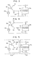
- a Darlingtion transistor TR 1 constituted by a Darlington connection of an output stage transistor 0 1 and a driving stage transistor Q 2 is driven by another driving transistor TR 2 so as to obtain a high DC amplification factor, for instance, as shown in Fig. 1.
- the Darlington transistor TR 1 is usually packaged on a radiator because it calls for cooling, whereas the driving transistor TR 2 is packaged on a printed circuit board on the side of control equipment.
- reference character PS indicates a driving power source, R a resistor, D a diode, C 1 , B i and E 1 the collector, base and emitter of the Darlington transistor TR 1 , and C 2 , B 2 and E 2 the collector, base and emitter of the driving transistor TR 2 .
- the oscillation has been prevented by connecting a capacitor CP of a suitable capacitance between the base and emitter of the Darlington transistor TR 1 as shown in an electric circuit diagram of Fig. 3 in which the Darlington transistor in Fig. 1 is indicated by a black box, or by connecting a resistor RG between the base 8 1 of the Darlington transistor TR 1 and the emitter E 2 of the driving transistor TR 2 as shown in Fig. 4;
- the former method has the defect that a transistor of large current capacity is required as the driving transistor TR 2 because a current flows through the capacitor CP, and the latter method has the defect that a forward voltage drop of the Darlington transistor TR 1 becomes large, resulting in increased loss.
- the present invention is intended to overcome such defects, and has for its object to prevent or reduce the aforementioned oscillation with a simple arrangement.
- a transistor amplifier circuit in which a transistor is connected to be driven by a driving transistor, the two transistors being interconnected via a diode which opposes oscillation in the circuit, characterised in that: the driven transistor has a relatively large input capacitance; an electrical connection between the two transistors is so long that if said diode were not provided oscillation would tend to occur between the inductance of said connection and the input capacitance of the driven transistor; and said diode is arranged and poled to conduct driving current which flows through the driving transistor to the driven transistor.
- the rectifying operation of the oscillation- opposing diode inhibits the transmission and reception of current necessary for oscillation.
- the current capacity value of the driving transistor need not be increased and loss does not increase, either.
- Fig. 5 is an electrical circuit diagram illustrating the principal part of an embodiment of the present invention. The parts corresponding to those in Fig. 1 are identifed by the same reference characters.
- Reference character D 1 indicates a diode for preventing oscillation, PCB a printed circuit board, and RD a radiator.
- the oscillation preventive diode D 1 of a polarity shown is connected between the collector C 1 of the Darlington transistor TR 1 and the collector C 2 of the driving transistor TR 2 .
- the oscillation preventive diode D 1 is connected at least either between the collectors of the Darlington transistor TR 1 and the driving transistor TR 2 , or between the base B 1 of the Darlington transistor TR 1 and the emitter E 2 of the driving transistor TR 2 , as indicated by the broken line 50 in Fig. 5. Its packaging is carried out on the printed circuit board PCB in practice.
- a circuit for increasing the switching speed of the Darlington transistor TR 1 is connected between the base B 1 of the Darlington transistor TR 1 and the emitter E 2 of the driving transistor TR 2 and, in such a case, it may be difficult or improper to connect the oscillation preventative diode D 1 at the position 50; in this case, the oscillation preventive diode D 1 is connected between the collectors of the Darlington transistor TR 1 and the driving transistor TR 2 .
- the present invention has been described as being applied to a transistor amplifier circuit arranged to drive a Darlington transistor by another transistor, the invention is not limited specifically thereto but may also be applied to a transistor amplifier circuit which drives an individual transistor of relatively large input capacitance by another transistor and is liable to oscillate due to large wire length between the two transistors. The same effect as mentioned previously can be obtained.
- the present invention has the advantage that oscillation can be prevented with an extremely simple arrangement, without the necessity of increasing the current capacity value of the driving transistor as in the case of the prior art circuit shown in Fig. 3 and without incurring an increase in loss as in the conventional circuit depicted in Fig. 4. Accordingly, the present invention, when applied to a servomotor driving power amplifier or the like, enhances its reliability, and hence is of great utility.
Landscapes
- Engineering & Computer Science (AREA)
- Power Engineering (AREA)
- Physics & Mathematics (AREA)
- Nonlinear Science (AREA)
- Amplifiers (AREA)
- Bipolar Integrated Circuits (AREA)
Claims (6)
Applications Claiming Priority (2)
| Application Number | Priority Date | Filing Date | Title |
|---|---|---|---|
| JP143858/80 | 1980-10-15 | ||
| JP55143858A JPS5767303A (en) | 1980-10-15 | 1980-10-15 | Transistor amplifying circuit |
Publications (3)
| Publication Number | Publication Date |
|---|---|
| EP0062679A1 EP0062679A1 (de) | 1982-10-20 |
| EP0062679A4 EP0062679A4 (de) | 1983-02-14 |
| EP0062679B1 true EP0062679B1 (de) | 1985-09-11 |
Family
ID=15348601
Family Applications (1)
| Application Number | Title | Priority Date | Filing Date |
|---|---|---|---|
| EP81902764A Expired EP0062679B1 (de) | 1980-10-15 | 1981-10-09 | Transistorverstärkerschaltung |
Country Status (4)
| Country | Link |
|---|---|
| EP (1) | EP0062679B1 (de) |
| JP (1) | JPS5767303A (de) |
| KR (1) | KR830008461A (de) |
| WO (1) | WO1982001449A1 (de) |
Families Citing this family (2)
| Publication number | Priority date | Publication date | Assignee | Title |
|---|---|---|---|---|
| US5095360A (en) * | 1990-10-10 | 1992-03-10 | Kyocera America, Inc. | Ceramic chip-resistant chamfered integrated circuit package |
| WO2023061387A1 (zh) * | 2021-10-13 | 2023-04-20 | 郭桥石 | 甲类放大装置 |
Citations (2)
| Publication number | Priority date | Publication date | Assignee | Title |
|---|---|---|---|---|
| JPS5061165A (de) * | 1973-09-25 | 1975-05-26 | ||
| JPS5428350U (de) * | 1977-07-28 | 1979-02-24 |
Family Cites Families (4)
| Publication number | Priority date | Publication date | Assignee | Title |
|---|---|---|---|---|
| US3348162A (en) * | 1965-02-26 | 1967-10-17 | Ibm | Circuit with selective nonlinear feedback |
| JPS466871A (de) * | 1971-05-18 | 1971-12-15 | ||
| JPS5135113B1 (de) * | 1971-06-29 | 1976-09-30 | ||
| JPS50124558A (de) * | 1974-03-18 | 1975-09-30 |
-
1980
- 1980-10-15 JP JP55143858A patent/JPS5767303A/ja active Pending
-
1981
- 1981-10-09 EP EP81902764A patent/EP0062679B1/de not_active Expired
- 1981-10-09 WO PCT/JP1981/000276 patent/WO1982001449A1/ja not_active Ceased
- 1981-10-15 KR KR1019810003901A patent/KR830008461A/ko not_active Ceased
Patent Citations (2)
| Publication number | Priority date | Publication date | Assignee | Title |
|---|---|---|---|---|
| JPS5061165A (de) * | 1973-09-25 | 1975-05-26 | ||
| JPS5428350U (de) * | 1977-07-28 | 1979-02-24 |
Also Published As
| Publication number | Publication date |
|---|---|
| EP0062679A1 (de) | 1982-10-20 |
| KR830008461A (ko) | 1983-11-18 |
| JPS5767303A (en) | 1982-04-23 |
| WO1982001449A1 (fr) | 1982-04-29 |
| EP0062679A4 (de) | 1983-02-14 |
Similar Documents
| Publication | Publication Date | Title |
|---|---|---|
| DE69508644T2 (de) | Halbleiter-Leistungsmodul und -Leistungswandlervorrichtung | |
| US5001373A (en) | Active clamp circuit with immunity to zener diode microplasmic noise | |
| KR930003176B1 (ko) | 접지해제 보호회로를 갖는 전자 회로장치 | |
| EP0181201B1 (de) | Treiberschaltung für einen bipolaren Darlington-Leistungstransistor | |
| US6483345B1 (en) | High speed level shift circuit for low voltage output | |
| JPS59186410A (ja) | 帰還型増幅器 | |
| US4275436A (en) | Converter bleeder circuit responsive to flux condition of filter inductor | |
| US4023069A (en) | Vertical deflection circuit | |
| EP0062679A1 (de) | Transistorverstärkerschaltung | |
| US20090251198A1 (en) | Circuit Arrangement and Method for Driving an Electronic Component With an Output Signal From a Microprocessor | |
| US4114054A (en) | Coupling circuit using a photocoupler | |
| US4456836A (en) | Gate circuit for gate turn-off thyristor | |
| US4588906A (en) | Regulator circuit | |
| JPH08162631A (ja) | Igbtモジュール構造 | |
| US6653864B2 (en) | Interface | |
| US4417130A (en) | Transistor type pulse welding device | |
| JPS6116631Y2 (de) | ||
| JPS6268319A (ja) | 誘導性負荷駆動回路 | |
| KR920010199B1 (ko) | 반도체 칩의 입출력단 구동특성의 개선방법 | |
| US3953747A (en) | AC wave switching circuit using at least one switching transistor | |
| KR960005980B1 (ko) | 오디오 회로 공용을 위한 스위칭 회로 | |
| JPS58215825A (ja) | 半導体論理回路 | |
| KR890002555Y1 (ko) | 파우어 트랜지스터 구동 회로 | |
| JPS63313891A (ja) | レ−ザ−ダイオ−ド駆動用半導体集積回路装置 | |
| JPH0368635B2 (de) |
Legal Events
| Date | Code | Title | Description |
|---|---|---|---|
| PUAI | Public reference made under article 153(3) epc to a published international application that has entered the european phase |
Free format text: ORIGINAL CODE: 0009012 |
|
| 17P | Request for examination filed |
Effective date: 19820611 |
|
| AK | Designated contracting states |
Designated state(s): DE FR GB |
|
| RAP1 | Party data changed (applicant data changed or rights of an application transferred) |
Owner name: FANUC LTD |
|
| GRAA | (expected) grant |
Free format text: ORIGINAL CODE: 0009210 |
|
| AK | Designated contracting states |
Designated state(s): DE FR GB |
|
| REF | Corresponds to: |
Ref document number: 3172245 Country of ref document: DE Date of ref document: 19851017 |
|
| ET | Fr: translation filed | ||
| PLBE | No opposition filed within time limit |
Free format text: ORIGINAL CODE: 0009261 |
|
| STAA | Information on the status of an ep patent application or granted ep patent |
Free format text: STATUS: NO OPPOSITION FILED WITHIN TIME LIMIT |
|
| 26N | No opposition filed | ||
| PG25 | Lapsed in a contracting state [announced via postgrant information from national office to epo] |
Ref country code: FR Free format text: LAPSE BECAUSE OF NON-PAYMENT OF DUE FEES Effective date: 19870630 |
|
| GBPC | Gb: european patent ceased through non-payment of renewal fee | ||
| PG25 | Lapsed in a contracting state [announced via postgrant information from national office to epo] |
Ref country code: DE Effective date: 19870701 |
|
| REG | Reference to a national code |
Ref country code: FR Ref legal event code: ST |
|
| PG25 | Lapsed in a contracting state [announced via postgrant information from national office to epo] |
Ref country code: GB Effective date: 19881121 |