EP0062949B1 - Emetteur de télévision - Google Patents
Emetteur de télévision Download PDFInfo
- Publication number
- EP0062949B1 EP0062949B1 EP82200414A EP82200414A EP0062949B1 EP 0062949 B1 EP0062949 B1 EP 0062949B1 EP 82200414 A EP82200414 A EP 82200414A EP 82200414 A EP82200414 A EP 82200414A EP 0062949 B1 EP0062949 B1 EP 0062949B1
- Authority
- EP
- European Patent Office
- Prior art keywords
- video signal
- klystron
- control electrode
- signal
- transmitter
- Prior art date
- Legal status (The legal status is an assumption and is not a legal conclusion. Google has not performed a legal analysis and makes no representation as to the accuracy of the status listed.)
- Expired
Links
- 239000013307 optical fiber Substances 0.000 claims description 6
- 230000008878 coupling Effects 0.000 claims description 3
- 238000010168 coupling process Methods 0.000 claims description 3
- 238000005859 coupling reaction Methods 0.000 claims description 3
- 230000000295 complement effect Effects 0.000 claims description 2
- 239000003990 capacitor Substances 0.000 description 7
- 230000003287 optical effect Effects 0.000 description 7
- 238000000034 method Methods 0.000 description 4
- 230000005540 biological transmission Effects 0.000 description 3
- 230000005855 radiation Effects 0.000 description 3
- 238000004804 winding Methods 0.000 description 3
- 239000002131 composite material Substances 0.000 description 2
- 238000010586 diagram Methods 0.000 description 2
- 230000000694 effects Effects 0.000 description 2
- 230000003321 amplification Effects 0.000 description 1
- 230000000903 blocking effect Effects 0.000 description 1
- 238000006243 chemical reaction Methods 0.000 description 1
- 239000000835 fiber Substances 0.000 description 1
- 239000003365 glass fiber Substances 0.000 description 1
- 238000002955 isolation Methods 0.000 description 1
- 238000003199 nucleic acid amplification method Methods 0.000 description 1
- 238000005070 sampling Methods 0.000 description 1
- 238000001228 spectrum Methods 0.000 description 1
- 230000001360 synchronised effect Effects 0.000 description 1
Images

Classifications
-
- H—ELECTRICITY
- H04—ELECTRIC COMMUNICATION TECHNIQUE
- H04N—PICTORIAL COMMUNICATION, e.g. TELEVISION
- H04N5/00—Details of television systems
- H04N5/38—Transmitter circuitry for the transmission of television signals according to analogue transmission standards
Definitions
- the invention relates to a television transmitter for transmitting amplitude modulated signals, the transmitter comprising a klystron amplifier, means for feeding the amplitude modulated video signal to the input cavity of the klystron, means for coupling the signal from the output cavity of the klystron to an antenna, and means for feeding the unmodulated video signal to a control electrode situated adjacent to the cathode of the klystron.
- a broadcast television signal normally comprises a carrier signal, an upper sideband having a bandwidth of between 4 and 6 MHz and a lower sideband having a bandwidth of 0.75-1.25 MHz.
- the lower sideband is referred to as a vestigial sideband.
- the higher frequencies which are produced in the lower sideband by the modulator may be filtered either before or after application to the klystron amplifier. However if the filter is situated at the output of the klystron amplifier it has to be constructed so as to be able to dissipate considerable energy and consequently it is desirable to filter the modulated signal before application to the klystron amplifier. If, however, the video signal is now applied to the control grid of the klystron the higher frequencies of the lower sideband may be reinserted by the modulation of the beam current density.
- the invention provides a television transmitter as described in the opening paragraph characterised in that said transmitter is so arranged that: the amplitude modulated signal fed to the input cavity of the klystron comprises a full sideband and a vestigial sideband; the bandwidth of the video signal applied to the grid of the klystron is less than or equal to the bandwidth of the vestigial sideband; and the means for feeding the unmodulated signal to the control electrode includes d.c. isolating means to isolate the cathode and electrode potential from the video signal source.
- the restriction of the bandwidth of the video signal applied to the control electrode of the klystron has two advantages. First the possibility of reinserting the higher frequencies into the vestigial sideband is reduced and second the power necessary to drive the control electrode is reduced. It has been found that the bandwidth of the video signal applied to the electrode may be further reduced to below 500 KHz, since the major part of the power in the video signal is in practice contained in the lower frequency components.
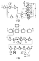
- the television transmitter shown in Figure 1 has an input terminal 1 to which, in operation, a composite video signal is applied.
- the terminal 1 is coupled to the input of a video processing circuit 2 whose output is connected via a line 3 to a first input of an amplitude modulator 4 and via a line 5 to a low pass filter 6.
- the output of a local oscillator 7 is connected to a second input of the amplitude modulator 4.
- the output signal from the modulator 4 is passed through a filter 8 which has a passband which covers the upper sideband, the carrier, and a portion or vestige of the lower sideband.
- the filter 8 is normally designated the vestigial sideband filter.
- the television signal to be transmitted should have a video bandwidth consistent with the television standard concerned for the upper sideband and 0.75 to 1.25 MHz for the lower or vestigial sideband.
- the output of the filter 8 is then fed to an R.F. amplifying circuit 9 which will include signal linearising and correcting circuitry both for amplitude and phase or delay, including that caused by the variation in the gain of the klystron as the beam current is varied, and frequency conversion circuitry to arrange the modulated signal into the desired transmission channel.
- the main power amplification takes place in a klystron amplifier 10.
- the klystron comprises an indirectly heated cathode 11, a control electrode 12 which may be in the form of a grid, as shown, or may be an annular electrode, an anode 13, an input cavity 14, a drift tube 15, an output cavity 16, a collector 17, and two intermediate cavities 18 and 19.
- the drift tube and collector are held at earth or near potential while a high negative voltage, normally between 10 and 30K Volts, is applied to the cathode.
- the anode is maintained at a potential between that of earth and that of the cathode in order to determine the basic operating conditions of the klystron.
- the output of the low pass filter 6 fed via a d.c. isolating circuit 20 to an amplifier 21 whose output is connected to the control electrode 12 of the klystron 10.
- the filter 6 restricts the bandwidth of the video signal fed to the control electrode 12 to not greater than that of the vestigial sideband.
- the d.c. isolating circuit 20 is included to isolate the control grid, which is at a potential close to that of the cathode, from the rest of the transmitter circuitry.
- the modulated and shaped video signal available at the output of the R.F. amplifier 9 is coupled to the input cavity 14 of the klystron 10 while the amplified signal is fed from the output cavity 16 of the klystron 10 to an antenna 22.
- the voltage excursion produced by the amplifier 21 may typically be from +200 volts to -700 volts with respect to the cathode potential and the grid 12 is located with respect to the cathode at the position where the grid at a potential of +700 volts the klystron would behave as if no grid was present. Consequently during the synchronising pulses when the potential on the control grid 12 is +700 volts the control grid 12 becomes effectively transparent and the beam circuit is that which would be present in the absence of the control grid 12. At lower potentials with respect to the cathode the beam current will be reduced.
- the voltage excursion produced by the amplifier 21 may typically be from 0 V to -1000 V with respect to the cathode potential, the control electrode 12 becoming effectively transparent when the potential is 0 V and hence the beam current becoming that which would be present in the absence of the control electrode.
- the embodiment described thus far has the disadvantage that there is a double modulation of the low frequency components of the video signal in the klystron. This causes a distortion in the output signal in which the low frequency components and synchronising pulses are increased in amplitude relative to the high frequency components.
- a high pass filter having a characteristic complementary to that of the low pass filter 6 may be inserted in the line 3. The high pass filter will substantially reduce the low frequency content of the signal applied to the modulator 4 and hence the double modulation.
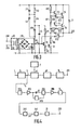
- the input terminal 1 is fed with the composite video signal which is fed to the video processing circuit 2.
- the output of the video processing circuit 2 is fed via a line 3 to the modulator 4, vestigial sideband filter 8 and R.F. amplifying circuit 9 which forms a conventional portion of a transmitter, the output of the R.F. amplifying circuit 9 being fed to a terminal 201 which is coupled to the input cavity of the klystron 10.
- the output of the video processing circuit 2 is also fed via a line 5 to a variable delay circuit 202 which is adjustable to enable the signal applied to the electrode 12 of the klystron 10 to be synchronised with that applied to the input. cavity 14.
- a variable delay circuit 202 which is adjustable to enable the signal applied to the electrode 12 of the klystron 10 to be synchronised with that applied to the input. cavity 14.
- the signal is fed via a buffer amplifier 203 and a capacitor C1 to a clamp circuit 204.
- the output of the amplifier 203 is also fed via a synchronising signal separator 205 to the clamp circuit 204.
- the output of the clamp circuit 204 is fed through a buffer amplifier 206 to the low pass filter 6.
- the restricted bandwidth video signal from the output of the low pass filter 6 is fed to a first input of a modulator 207 whose second input is fed from a carrier frequency oscillator 208.
- the modulated video signal produced at the output of the modulator 207 is fed via a buffer amplifier 209 to the d.c. isolating circuit 20.
- the d.c. isolating circuit may comprise a transformer having the desired voltage rating i.e. up to 30 K Volts, between its primary and secondary windings and from the primary and secondary windings to its core and case.
- the output from the d.c. isolating circuit 20 is fed to a demodulator 210 and the demodulated signal is fed to the control grid 12 of the klystron 10 via the amplifier 21.
- the gain of amplifier 203 is adjustable to set the amplitude of the video signal to 1 Volt peak to peak and the clamping circuit 204 then sets the peak value of the synchronising signal at 0 volts.
- the gain of the modulator 207 may be adjusted so that the voltage of the demodulated signal at the input to the amplifier 21 varies between -0.8 volts and -5.8 volts as shown by the waveform in Figure 2.
- FIG. 3 is a circuit diagram of an amplifier suitable for this purpose.
- Figure 3 also shows the d.c. isolating circuit 20 in the form of a transformer TR1 and the demodulator 210.
- the modulated video signal is applied to the primary of transformer TR1 via two input terminals 218 and 219 and the' transformer secondary winding is connected to the demodulator 210.
- the demodulator 210 comprises a bridge rectifier BR1 and a capacitor C2.
- the voltage on the capacitor C2 is applied via a resistor R1 to the base of an npn transistor T1.
- the emitter of transistor T1 is connected to the base of an npn transistor T2 and via a resistor R2 to the negative supply rail -V.
- the series arrangement of two resistors R3 and R4 and a voltage reference diode VR1 is connected between the positive supply rail +V and the negative supply rail.
- the series arrangement of two capacitors C3 and C4 is connected between the positive and negative supply rails with the junction of the capacitors being connected to the junction of resistors R3 and R4.
- the junction of resistor R4 and the voltage reference diode VR1 is connected via a resistor R5 to the collector of transistor T1.
- the emitter of transistor T2 is connected to the negative supply rail while its collector is connected to the positive supply rail via the series arrangement of three resistors R6, R7 and R8.
- resistors R7 and R8 are connected to the base of an npn transistor T3 whose collector is connected to the positive supply rail.
- the emitter of transistor T3 is connected to the base of an npn transistor T4, to the collector of an npn transistor T5, and via a resistor R9 to its own base.
- the base of transistor T5 is connected to the junction of resistors R6 and. R7 and via a resistor R10 to its own emitter which in turn is connected to the base of an npn transistor T6 and to one end of a resistor R11 the other end of which is connected to the emitter of transistor T6.
- the collector of transistor T4 is connected to the positive supply rail while its emitter is connected to the collector of transistor T6 and via a resistor R12 to the emitter of transistor T3.
- the emitter of transistor T6 is conected to a terminal 220 which forms the amplifier output and which is connected to the control grid 12 of the klystron 10.
- a first diode D1 is connected between the output terminal 220 and the positive supply rail while a second diode D2 is connected between the output terminal 220 and the junction of resistors R6 and R7.
- a resistor R13 is connected between the emitter of transistor T6 and the base of transistor T1.
- the demodulated signal is produced across capacitor C2 and is of the form shown in Figure 2 at the output of the demodulator 210.
- the supply voltage between the positive and negative supply rails is 800 volts and the negative supply rail is connected to the cathode potential of the klystron 10, that is -30 K Volts.
- the output voltage at terminal 220 varies between +200 volts and +700 volts with respect to the cathode potential of the klystron 10.
- Transistors T3 and T6 form a high voltage emitter follower stage.
- the potential divider formed by resistors R7 and R8 is connected so that the maximum voltage across any one of these transistors is limited to 400 volts.
- the emitter follower stage is fed from transistor T2 which is in turn driven by transistor T1.
- Negative feedback from the output of the amplifier to the base of transistor T1 is provided via resistor R13 and the gain of the amplifier is substantially equal to
- the diodes D1 and D2 are included to protect the amplifier from the effects of voltage flash- overs in the klystron 10.
- Diode D1 prevents the voltage at terminal 220 from becoming more positive than +V (800 V) and diode D2 prevents reverse biassing of the transistors T3 to T6.
- control electrode 12 When the control electrode 12 is in the form of a ring electrode a similar amplifier may be used having its positive supply rail connected to the cathode potential and with the addition of a load resistor connected between terminal 220 and the negative supply rail.
- Figure 4 illustrates an alternative method of applying the restricted bandwidth video signal to the control grid 12 of the klystron 10.
- the arrangement shown in Figure 4 is identical to that shown in Figure 2 until the output of the low pass filter 6.
- the output from the low pass filter 6 is fed to a generator of optical signals 240 such as a light emitting diode or a laser.
- the optical signal generator 240 takes the video signal from the output of the low pass filter 6 and converts it into an optical signal which is passed through a glass fibre light guide 241 and which is detected by an optical detector 242.
- the optical detector 242 converts the received optical signal into an electrical signal and applies this signal to the amplifying circuit 21.
- the optical detector 242 and amplifier 21 are at the potential of the cathode of the klystron 10 i.e. between -10 and -30 K volts and are d.c. isolated from the rest of the transmitter by the optical fibre 241.
- Figure 5 illustrates a further alternative method of applying the restricted bandwidth video signal to the control electrode 12 of the klystron 12.
- the arrangement shown in Figure 5 is identical to that shown in Figure 4 until the output of the low pass filter 6 which defines the bandwidth of the signal to be applied to the grid of the klystron.
- the output of the filter is fed via an amplifier 501 to a first input of a comparator 502 while the output of a ramp generator 503 is applied to a second input of the comparator 502.
- the output of comparator 502 comprises a pulse whose width is determined by the period during which the output of amplifier 501 is greater than that of the ramp generator 503.
- the amplifier 501, comparator 502 and ramp generator 503 form a pulse width modulator 504 whose output is fed via a driver circuit 505 to a light emitting diode D1.
- the frequency of the output of the ramp generator 503 must be at least twice the bandwidth of the signal to be applied to the grid of the klystron and may conveniently be of the order of 1 MHz.
- the light emitting diode D1 emits pulses of radiation, which may be in the infra-red or visible regions of the spectrum, in response to the current pulses passed through it by the driver circuit 505.
- the emitted radiation pulses are passed along an optical fibre link 510 to a photo-detector D2 which is connected to the input of a limiting amplifier 506.
- the limiting amplifier 506 regenerates the pulse waveform which was degraded in the transmission along the optical fibre link 510.
- the pulses at the output of the limiting amplifier 506 are fed to a low pass filter 507 which produces a demodulated video signal at its output.
- the output of the low pass filter 507 varies between 0 volts and +V volts where these two potentials are the supply potentials to the limiting amplifier 506.
- a level shifting circuit 508 is included between the output of the filter 507 and the input of amplifier 21.
- the cut-off frequency of the low pass filter 507 may conveniently be 500 KHz which is well below the 1 MHz sampling frequency but allows sufficient bandwidth for some variation of the Bandwidth of the video signal.
- the actual video signal bandwidth is mainly determined by the cut-off frequency of the low pass filter 6.
- the fibre optic link 510 provides electrical isolation between the video signal source and the cathode and control electrode potential of the klystron. By pulse width modulating the video signal before applying it to the light emitting diode D1 the linearity of the diode characteristic becomes less important and relatively inexpensive optical fibre may be used for the transmission link.
Landscapes
- Engineering & Computer Science (AREA)
- Multimedia (AREA)
- Signal Processing (AREA)
- Amplitude Modulation (AREA)
- Transmitters (AREA)
Claims (10)
Applications Claiming Priority (4)
| Application Number | Priority Date | Filing Date | Title |
|---|---|---|---|
| GB8111894 | 1981-04-15 | ||
| GB8111894 | 1981-04-15 | ||
| GB8207017 | 1982-03-10 | ||
| GB8207017A GB2096849A (en) | 1981-04-15 | 1982-03-10 | Television transmitter |
Publications (2)
| Publication Number | Publication Date |
|---|---|
| EP0062949A1 EP0062949A1 (fr) | 1982-10-20 |
| EP0062949B1 true EP0062949B1 (fr) | 1984-10-24 |
Family
ID=26279149
Family Applications (1)
| Application Number | Title | Priority Date | Filing Date |
|---|---|---|---|
| EP82200414A Expired EP0062949B1 (fr) | 1981-04-15 | 1982-04-02 | Emetteur de télévision |
Country Status (6)
| Country | Link |
|---|---|
| US (1) | US4470068A (fr) |
| EP (1) | EP0062949B1 (fr) |
| CA (1) | CA1181164A (fr) |
| DE (1) | DE3261032D1 (fr) |
| ES (1) | ES8304395A1 (fr) |
| GB (1) | GB2096849A (fr) |
Families Citing this family (6)
| Publication number | Priority date | Publication date | Assignee | Title |
|---|---|---|---|---|
| GB8403067D0 (en) * | 1984-02-06 | 1984-03-07 | Indep Broadcasting Authority | Broadcast signal transmitters |
| US4877499A (en) * | 1984-11-05 | 1989-10-31 | The Dow Chemical Company | Membrane unit for electrolytic cell |
| GB2179216B (en) * | 1985-07-02 | 1989-04-26 | English Electric Valve Co Ltd | Amplifying arrangements |
| GB2211045B (en) * | 1987-10-10 | 1991-08-21 | Marconi Co Ltd | Linearity adjusting circuit |
| US6457178B1 (en) | 1998-03-17 | 2002-09-24 | Scientific-Atlanta, Inc. | Pulse width modulator for communication system including fiber optic communications |
| US20060140644A1 (en) * | 2004-12-23 | 2006-06-29 | Paolella Arthur C | High performance, high efficiency fiber optic link for analog and RF systems |
Family Cites Families (4)
| Publication number | Priority date | Publication date | Assignee | Title |
|---|---|---|---|---|
| US3473125A (en) * | 1967-12-19 | 1969-10-14 | Csf | Klystron am transmitters |
| JPS5145932B1 (fr) * | 1969-11-19 | 1976-12-06 | ||
| US3955155A (en) * | 1974-12-23 | 1976-05-04 | Rca Corporation | Amplitude modulation system |
| US4300237A (en) * | 1977-10-03 | 1981-11-10 | Morgan Harvey L | Single sideband modulation |
-
1982
- 1982-03-10 GB GB8207017A patent/GB2096849A/en not_active Withdrawn
- 1982-03-31 CA CA000400006A patent/CA1181164A/fr not_active Expired
- 1982-04-02 ES ES511099A patent/ES8304395A1/es not_active Expired
- 1982-04-02 EP EP82200414A patent/EP0062949B1/fr not_active Expired
- 1982-04-02 DE DE8282200414T patent/DE3261032D1/de not_active Expired
- 1982-04-05 US US06/365,758 patent/US4470068A/en not_active Expired - Fee Related
Also Published As
| Publication number | Publication date |
|---|---|
| EP0062949A1 (fr) | 1982-10-20 |
| ES511099A0 (es) | 1983-02-16 |
| ES8304395A1 (es) | 1983-02-16 |
| CA1181164A (fr) | 1985-01-15 |
| GB2096849A (en) | 1982-10-20 |
| US4470068A (en) | 1984-09-04 |
| DE3261032D1 (en) | 1984-11-29 |
Similar Documents
| Publication | Publication Date | Title |
|---|---|---|
| GB1256789A (fr) | ||
| WO1982002632A1 (fr) | Dispositif de communication optique pour la reduction de la distorsion harmonique | |
| US3506920A (en) | High efficiency transformer utilizing pulse duration modulation to eliminate audio-rf transformer coupling | |
| EP0062949B1 (fr) | Emetteur de télévision | |
| US4097896A (en) | Sync separator circuit | |
| GB634501A (en) | Television signal-translating system | |
| EP0689305B1 (fr) | Emetteur optique pour système de transmission optique à sous-porteuses multiplexées | |
| US4435725A (en) | Color signal processing circuit to reduce cross-color disturbance and color fringing | |
| US5278515A (en) | High bandwidth information channel with optocoupling isolation | |
| US6671465B1 (en) | Apparatus and methods for improving linearity and noise performance of an optical source | |
| US4031430A (en) | Vertical deflection circuit | |
| US3764925A (en) | Demodulator circuit | |
| US5448392A (en) | Process for the optical transmission of a multiplex of electrical carriers and apparatus for performing such a process | |
| US2246947A (en) | Automatic gain control | |
| US4538180A (en) | System for non linearity correction by intermediate frequency premodulation in television equipment | |
| US3535444A (en) | Noise immune video circuits | |
| JPS6017193B2 (ja) | 直流再生回路 | |
| US2240507A (en) | Television synchronizing and control system | |
| Pophillat | Optical modulation depth improvement in SCM lightwave systems using a dissymmetrization scheme | |
| JP2530229B2 (ja) | 映像信号クランプ回路 | |
| US2469606A (en) | Video signal level control | |
| US3439115A (en) | Keyed automatic gain control circuit for television receivers | |
| US2182043A (en) | Television and like system | |
| JP2751162B2 (ja) | 光伝送方式 | |
| CA1100227A (fr) | Traduction non-disponible |
Legal Events
| Date | Code | Title | Description |
|---|---|---|---|
| PUAI | Public reference made under article 153(3) epc to a published international application that has entered the european phase |
Free format text: ORIGINAL CODE: 0009012 |
|
| 17P | Request for examination filed |
Effective date: 19820402 |
|
| AK | Designated contracting states |
Designated state(s): CH DE FR GB LI SE |
|
| GRAA | (expected) grant |
Free format text: ORIGINAL CODE: 0009210 |
|
| AK | Designated contracting states |
Designated state(s): CH DE FR GB LI SE |
|
| PG25 | Lapsed in a contracting state [announced via postgrant information from national office to epo] |
Ref country code: LI Effective date: 19841024 Ref country code: CH Effective date: 19841024 |
|
| REF | Corresponds to: |
Ref document number: 3261032 Country of ref document: DE Date of ref document: 19841129 |
|
| ET | Fr: translation filed | ||
| ET3 | Fr: translation filed ** decision concerning opposition | ||
| REG | Reference to a national code |
Ref country code: CH Ref legal event code: PL |
|
| PLBE | No opposition filed within time limit |
Free format text: ORIGINAL CODE: 0009261 |
|
| STAA | Information on the status of an ep patent application or granted ep patent |
Free format text: STATUS: NO OPPOSITION FILED WITHIN TIME LIMIT |
|
| 26N | No opposition filed | ||
| PGFP | Annual fee paid to national office [announced via postgrant information from national office to epo] |
Ref country code: GB Payment date: 19910402 Year of fee payment: 10 |
|
| PGFP | Annual fee paid to national office [announced via postgrant information from national office to epo] |
Ref country code: FR Payment date: 19910419 Year of fee payment: 10 |
|
| PGFP | Annual fee paid to national office [announced via postgrant information from national office to epo] |
Ref country code: SE Payment date: 19910425 Year of fee payment: 10 |
|
| PGFP | Annual fee paid to national office [announced via postgrant information from national office to epo] |
Ref country code: DE Payment date: 19910625 Year of fee payment: 10 |
|
| PG25 | Lapsed in a contracting state [announced via postgrant information from national office to epo] |
Ref country code: GB Effective date: 19920402 |
|
| PG25 | Lapsed in a contracting state [announced via postgrant information from national office to epo] |
Ref country code: SE Effective date: 19920403 |
|
| GBPC | Gb: european patent ceased through non-payment of renewal fee | ||
| PG25 | Lapsed in a contracting state [announced via postgrant information from national office to epo] |
Ref country code: FR Effective date: 19921230 |
|
| PG25 | Lapsed in a contracting state [announced via postgrant information from national office to epo] |
Ref country code: DE Effective date: 19930101 |
|
| REG | Reference to a national code |
Ref country code: FR Ref legal event code: ST |
|
| EUG | Se: european patent has lapsed |
Ref document number: 82200414.9 Effective date: 19921108 |