EP0063061A1 - Farbbildabtasteinrichtung unter Verwendung von elektrischer Ladungsübertragung und eine solche Einrichtung enthaltende Fernsehkamera - Google Patents
Farbbildabtasteinrichtung unter Verwendung von elektrischer Ladungsübertragung und eine solche Einrichtung enthaltende Fernsehkamera Download PDFInfo
- Publication number
- EP0063061A1 EP0063061A1 EP82400462A EP82400462A EP0063061A1 EP 0063061 A1 EP0063061 A1 EP 0063061A1 EP 82400462 A EP82400462 A EP 82400462A EP 82400462 A EP82400462 A EP 82400462A EP 0063061 A1 EP0063061 A1 EP 0063061A1
- Authority
- EP
- European Patent Office
- Prior art keywords
- points
- line
- photosensitive
- memories
- column
- Prior art date
- Legal status (The legal status is an assumption and is not a legal conclusion. Google has not performed a legal analysis and makes no representation as to the accuracy of the status listed.)
- Granted
Links
- 238000012546 transfer Methods 0.000 title claims description 18
- 239000011159 matrix material Substances 0.000 claims abstract description 26
- 230000015654 memory Effects 0.000 claims description 54
- 239000000758 substrate Substances 0.000 claims description 24
- 238000002955 isolation Methods 0.000 claims description 21
- 239000004065 semiconductor Substances 0.000 claims description 17
- 239000003086 colorant Substances 0.000 claims description 13
- 238000010191 image analysis Methods 0.000 claims description 7
- 230000006870 function Effects 0.000 claims description 5
- 238000009413 insulation Methods 0.000 claims description 4
- 238000000034 method Methods 0.000 claims description 4
- 230000008569 process Effects 0.000 claims description 4
- 238000005286 illumination Methods 0.000 claims description 3
- 229910052782 aluminium Inorganic materials 0.000 claims description 2
- XAGFODPZIPBFFR-UHFFFAOYSA-N aluminium Chemical compound [Al] XAGFODPZIPBFFR-UHFFFAOYSA-N 0.000 claims description 2
- 239000003990 capacitor Substances 0.000 claims 1
- 238000004458 analytical method Methods 0.000 abstract description 5
- 239000010410 layer Substances 0.000 description 10
- 230000004888 barrier function Effects 0.000 description 7
- 238000010586 diagram Methods 0.000 description 7
- 239000012212 insulator Substances 0.000 description 5
- 230000035945 sensitivity Effects 0.000 description 4
- 241000238097 Callinectes sapidus Species 0.000 description 3
- 230000010354 integration Effects 0.000 description 3
- 230000003405 preventing effect Effects 0.000 description 3
- 230000008901 benefit Effects 0.000 description 2
- 239000004020 conductor Substances 0.000 description 2
- 238000002347 injection Methods 0.000 description 2
- 239000007924 injection Substances 0.000 description 2
- 238000004519 manufacturing process Methods 0.000 description 2
- 230000008520 organization Effects 0.000 description 2
- 230000003071 parasitic effect Effects 0.000 description 2
- 230000005855 radiation Effects 0.000 description 2
- 238000000926 separation method Methods 0.000 description 2
- VYPSYNLAJGMNEJ-UHFFFAOYSA-N Silicium dioxide Chemical compound O=[Si]=O VYPSYNLAJGMNEJ-UHFFFAOYSA-N 0.000 description 1
- 240000008042 Zea mays Species 0.000 description 1
- 238000010521 absorption reaction Methods 0.000 description 1
- 230000000295 complement effect Effects 0.000 description 1
- 230000008878 coupling Effects 0.000 description 1
- 238000010168 coupling process Methods 0.000 description 1
- 238000005859 coupling reaction Methods 0.000 description 1
- 238000001514 detection method Methods 0.000 description 1
- 238000011161 development Methods 0.000 description 1
- 238000007599 discharging Methods 0.000 description 1
- 238000009826 distribution Methods 0.000 description 1
- 230000008030 elimination Effects 0.000 description 1
- 238000003379 elimination reaction Methods 0.000 description 1
- 230000001965 increasing effect Effects 0.000 description 1
- 230000009545 invasion Effects 0.000 description 1
- 229910052751 metal Inorganic materials 0.000 description 1
- 239000002184 metal Substances 0.000 description 1
- 238000001465 metallisation Methods 0.000 description 1
- 230000003287 optical effect Effects 0.000 description 1
- 229910021420 polycrystalline silicon Inorganic materials 0.000 description 1
- 230000002829 reductive effect Effects 0.000 description 1
- 238000009877 rendering Methods 0.000 description 1
- 230000002441 reversible effect Effects 0.000 description 1
- 229910052710 silicon Inorganic materials 0.000 description 1
- 239000010703 silicon Substances 0.000 description 1
- 229910052814 silicon oxide Inorganic materials 0.000 description 1
- 239000002356 single layer Substances 0.000 description 1
- 239000007787 solid Substances 0.000 description 1
- 239000000243 solution Substances 0.000 description 1
- 238000003860 storage Methods 0.000 description 1
Images


Classifications
-
- H—ELECTRICITY
- H10—SEMICONDUCTOR DEVICES; ELECTRIC SOLID-STATE DEVICES NOT OTHERWISE PROVIDED FOR
- H10F—INORGANIC SEMICONDUCTOR DEVICES SENSITIVE TO INFRARED RADIATION, LIGHT, ELECTROMAGNETIC RADIATION OF SHORTER WAVELENGTH OR CORPUSCULAR RADIATION
- H10F39/00—Integrated devices, or assemblies of multiple devices, comprising at least one element covered by group H10F30/00, e.g. radiation detectors comprising photodiode arrays
- H10F39/10—Integrated devices
- H10F39/12—Image sensors
- H10F39/18—Complementary metal-oxide-semiconductor [CMOS] image sensors; Photodiode array image sensors
- H10F39/182—Colour image sensors
-
- H—ELECTRICITY
- H04—ELECTRIC COMMUNICATION TECHNIQUE
- H04N—PICTORIAL COMMUNICATION, e.g. TELEVISION
- H04N25/00—Circuitry of solid-state image sensors [SSIS]; Control thereof
- H04N25/10—Circuitry of solid-state image sensors [SSIS]; Control thereof for transforming different wavelengths into image signals
- H04N25/11—Arrangement of colour filter arrays [CFA]; Filter mosaics
- H04N25/13—Arrangement of colour filter arrays [CFA]; Filter mosaics characterised by the spectral characteristics of the filter elements
- H04N25/134—Arrangement of colour filter arrays [CFA]; Filter mosaics characterised by the spectral characteristics of the filter elements based on three different wavelength filter elements
-
- H—ELECTRICITY
- H04—ELECTRIC COMMUNICATION TECHNIQUE
- H04N—PICTORIAL COMMUNICATION, e.g. TELEVISION
- H04N25/00—Circuitry of solid-state image sensors [SSIS]; Control thereof
- H04N25/70—SSIS architectures; Circuits associated therewith
- H04N25/71—Charge-coupled device [CCD] sensors; Charge-transfer registers specially adapted for CCD sensors
- H04N25/745—Circuitry for generating timing or clock signals
-
- H—ELECTRICITY
- H04—ELECTRIC COMMUNICATION TECHNIQUE
- H04N—PICTORIAL COMMUNICATION, e.g. TELEVISION
- H04N25/00—Circuitry of solid-state image sensors [SSIS]; Control thereof
- H04N25/70—SSIS architectures; Circuits associated therewith
- H04N25/76—Addressed sensors, e.g. MOS or CMOS sensors
- H04N25/767—Horizontal readout lines, multiplexers or registers
-
- H—ELECTRICITY
- H04—ELECTRIC COMMUNICATION TECHNIQUE
- H04N—PICTORIAL COMMUNICATION, e.g. TELEVISION
- H04N25/00—Circuitry of solid-state image sensors [SSIS]; Control thereof
- H04N25/70—SSIS architectures; Circuits associated therewith
- H04N25/76—Addressed sensors, e.g. MOS or CMOS sensors
- H04N25/7795—Circuitry for generating timing or clock signals
-
- H—ELECTRICITY
- H04—ELECTRIC COMMUNICATION TECHNIQUE
- H04N—PICTORIAL COMMUNICATION, e.g. TELEVISION
- H04N25/00—Circuitry of solid-state image sensors [SSIS]; Control thereof
- H04N25/70—SSIS architectures; Circuits associated therewith
- H04N25/76—Addressed sensors, e.g. MOS or CMOS sensors
- H04N25/78—Readout circuits for addressed sensors, e.g. output amplifiers or A/D converters
Definitions
- the present invention relates to the field of electrical analysis of light images using charge transfer in a semiconductor; it relates to a device more particularly suited to the analysis of color images.
- Various solid state devices are known for analyzing a light image, which are intended to be used in a television camera to provide an electrical video signal. They are distinguished by the embodiment of the photosensitive area on the one hand, and the system for reading and discharging the charges created by the image, on the other hand.
- the present invention relates to improvements to the structure of the line transfer device described above, aimed at adapting it to the analysis of color images.
- the invention also relates to a television camera comprising such an image analysis device.
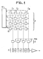
- FIG. 1 therefore represents the general organization of a line transfer structure, as described in the aforementioned French patent application.
- This structure mainly comprises a photosensitive zone 1, a line memory 2 and an analog shift register 3 for output.
- the photosensitive zone 1 receives the light image to be analyzed and transforms it into electrical charges. It should be noted that the aim here is by light image, the detection not only of the visible wavelengths but also of those which surround them, in particular in the infrared.
- the photosensitive zone is constituted by a plurality of elementary zones 15, also called below dots, arranged in N lines, identified L 1 , L 2 ... L N , and M columns, identified C 1 , C 2 ' .. C ,, and forming a matrix.
- the photosensitive points of the same line are linked together and connected to a control device 14, making it possible to address the lines one after the other; this device is constituted for example by a shift register of the MOS type.
- the photosensitive dots 15 of the same column are connected to the same connection, hereinafter called connection column, to line memory 2.
- the line memory 2 therefore receives in parallel the charges created in each of the photosensitive points 15 of the same line, then it also transfers them in parallel to the register 3, which is an analog shift register, of the CCD type, and which therefore provides the information, received in parallel, in serial mode; this information constitutes the video signal for analyzing the optical image received on the photosensitive zone 1.
- the content of the line memory 2 is transferred to the shift register 3, the input of the line memory being then closed.
- the next step corresponds to the line feed time during which the content of the line memory 2 is poured into the register 3, the latter having been completely read during the previous step.
- the selection of a line, its transfer to the line memory and then to the shift register are performed entirely during the return time.
- line time line being reserved for the updating of the reading means, which is all the better the longer it is, and for the serial evacuation of the shift register.
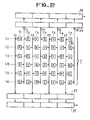
- FIG. 2 represents a first embodiment of the device according to the invention.
- the photosensitive matrix 1 has been diagrammed by its elementary zones, or points, 15, arranged in rows L (for example six rows L to L6 in the figure) and in columns C (for example seven columns C 1 to C 7 ).
- Each of the photosensitive dots is, as is known for taking a color photograph, covered with a colored filter so that it allows only one of three colors to pass, for example green, red or blue; in the figure, the photosensitive points 15 are marked R, G or B depending on whether they detect red, green or blue.
- the filters are distributed according to an inter-row staggered arrangement in which the points V, sensitive to green, more simply called “green points", are the most numerous because, as is known, it is those which give a maximum of sensitivity and therefore which are mainly used to obtain a luminance signal; moreover, the staggered arrangement makes it possible, as is also known, to increase the apparent resolution.
- This arrangement therefore consists of having a green point every two photosensitive points of each line, and of arranging these green points staggered from one line to another; on each line, the remaining photosensitive dots are alternately green or blue: we thus obtain the repetition of the green-red-green-blue sequence.
- the line memory 2 of FIG. 1 is here broken down into two memories, respectively 27 and 29, located on either side of the photosensitive matrix 1.
- One of these line memories (27) is connected to the connections of column of odd rank (noted c l , c 3 , c 5 and c 7 in the figure) while the other row memory (29) is connected to the column connections of even rank (c 2 , c 4 , c 6 and c 8 ).
- All the photosensitive points of the odd lines (L 1 , L 3 , L 5 ) are connected to a column connection which is on their left, all photosensitive dots of an even line (L 2 , L 4 ' L 6 ) are connected to the column connection which is on their right, with a line L starting with a green point, the column c 1 being located to its left . It can thus be seen that all the green dots are connected to the column connections of odd rank and therefore to the same row memory (27), the other photosensitive points being arranged so that the even column connections provide the color red. (columns c 2 and c 6 ) and the others, the blue color (c 4 and cg).
- each of the line memories 27 and 29 is connected in parallel an output register, respectively 37 and 39, analogous to the register 3 of FIG. 1.
- the register 37 which is connected to the memory 27 provides an electrical signal representing the only green color, which makes it possible to deduce therefrom the luminance signal; register 39 alternately supplies the blue chrominance signal and then the red chrominance signal, which can thus be easily separated downstream from the analysis device.
- This structure by reading the charges in two different directions, therefore makes it possible to facilitate the development of the luminance signal and the separation of the chrominance components.
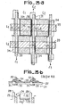
- FIG. 3a represents an embodiment of a matrix of photosensitive points capable of being used in the device of FIG. 2.
- a semiconductor substrate (not shown), in silicon for example, covered with an insulating layer, in silicon oxide for example, several conductive deposits 33, called below as the different deposits conductors of the device, electrodes or grids, possibly semi-transparent metallic or of polycrystalline silicon, parallel, representing the lines L of the matrix 1 of FIG. 2 (the lines L, and L 2 of the preceding figure, for example) and constituting with the semiconductor substrate and the insulator, photodetector MOS capacities.
- columns C of. the matrix (by example C ,, C 2 and C3) are placed grids 34, brought to a constant potential, which constitute a screen for the charges, according to a process described in more detail below.
- the device also includes, under each of the screen gates 34, a strip 35 produced in the semiconductor substrate, by doping for example, constituting a diode making it possible to read the different photosensitive points connected to the column considered.
- isolation barriers 31 in the form of vertical slots, shown in the figure in double lines, the horizontal parts of which are substantially in the middle of the space separating two grids 33, and the vertical parts are alternately left or right of the screen grids 34, without crossing them.
- Each of the isolation barriers 31 can be produced by a local excess thickness of the insulator, possibly accompanied by an overdoping of the semiconductor substrate, of the same type of conductivity as the latter (for example P overdoping for a P substrate), the overdoping intervening under the oxide excess thickness.
- a photosensitive point has been shown in thick lines, identified 30: it is bounded horizontally by the isolation barrier 31, on one of its vertical sides (right side in the example of the figure) by the same isolation barrier, and on its other. vertical side by the screen grid 34. According to a process described below, point 30 is read by the column diode 35 located to its left as indicated by an arrow 36 in the figure.
- each of the screen grids 34 is not in the form of a rectangular strip, but slightly in the form of vertical slots, like the isolation barriers 31 but of much smaller amplitude, in order to allow a maximum photosensitive surface: in fact, there is a minimum width for the screen grid between the photosensitive dot and the reading diode 35, but this width is of course not required. only on the side where this point is read: for example on the left side (arrow 36) for point 30 in the figure.
- the photosensitive point 30 is therefore formed of an MOS capacitance (semiconductor substrate, insulator and grid 33) constituting a first charge collection zone, and a second charge collection zone marked 38, consisting of two parts located between the grid 33 and the isolation barriers 30.
- MOS capacitance semiconductor substrate, insulator and grid 33
- the MOS capacity has a large charge storage capacity and thus makes it possible to obtain good dynamics for each photosensitive point, but grid 33 has greater absorption for the weak wavelengths, which are overcome by the second charge collection zone.
- a photodiode is formed in this zone 38, for example by doping the substrate, making it possible to increase the sensitivity of the point.
- This photodiode can be produced only in the space 38 between the grid 33 and the isolation barriers 30; it can also extend under the gate 33 in order to improve the electrical coupling between MOS capacitance and photodiode.
- These different embodiments of the second charge collection zone are also applicable to the different embodiments of the photosensitive matrix, described below.
- FIG. 3b represents a sectional view of FIG. 3a produced along a line AA, intersecting the photosensitive point 30 at the level of the MOS capacity grid 33.
- the structure of the device of FIG. 3a appears more clearly: it is produced in a semiconductor substrate 21, covered with an insulating layer 22, two isolation barriers 31 by excess thickness of insulator and a reading diode 35 to the right of each of the barriers 31, by doping the substrate.
- On the insulating layer 22 are deposited the screen grids 34 at the edge and to the right of the isolation barriers 31.
- the grid of the MOS capacity 33 extends over the substrate and above the screen grids 34, via 'a layer of insulation, not shown for clarity of the drawing.
- the device further comprises a metallization 32 deposited on the grid 33, by means of an insulating layer, at right of each of the diodes 35 and shown only in Figure 3b.
- These metal strips 32 have the function of constituting a screen opaque to light radiation which would be liable to create parasitic charges in the reading diodes 35. They can be made, for example, of aluminum.
- FIG. 4 represents another embodiment of the device according to the invention, suitable for the case where the reading of the photosensitive zone is done by interlaced half-frames, that is to say starting with the half-frame constituted by the odd order lines (odd half frame) then following by the half frame constituted by the even order lines (even half frame).
- each of the lines of a device such as that of FIG. 2 should be split to obtain an identical signal for each half-frame, which is necessary for good image quality on rendering .
- FIG. 4 there is a matrix 1 of six rows (L) and six columns (C) of photosensitive dots 15 to each of which is assigned a color (R, G or B), the green photosensitive dots being distributed in the same way as before.
- the remaining points are distributed so that a line is only two-color (green..and blue or green and red), the color information varying only once every two lines: for example line L 1 comprises alternately a green point and a blue point, and no red point; line L 2 alternately comprises red and green points, and no blue point; the same for line L 3 ; the lines L 4 and L 5 are again alternately blue and green, the line L 6 being alternately red and green, the point of the line L 1 and of the column CI being for example a blue point.
- the signal collected on each of the columns can be directed either to the line memory 27 or to the line memory 29.
- the devices 47 and 49 appropriately, described in more detail below, it is obtained in line memory 27 and therefore at the output of the associated shift register 37, only a signal representing the green chrominance information from which the luminance information is deduced, and on the line memory 29 and therefore at the output of the shift register 39 , successively a blue line then a red line in the same half-frame. The color separation is then complete and the alternation of red and then blue lines is adapted to the SECAM process.
- Figure 4a an alternative embodiment which consists of grouping the column connections in pairs between the columns of photosensitive dots, which increases the photosensitive area compared to that which is reserved for reading.
- the switching device 47 is constituted by six switching devices, for example MOS transistors, placed respectively on the six columns (C 1 to C6), those which are placed on the odd columns, marked 41 , being controlled by a potential 0 p applied to their grid, and those placed on the even columns, marked 42, are controlled by a potential ⁇ I also applied to their grid.
- the switching device 49 is made up of six MOS transistors interposed on the six columns C to C 6 respectively, the transistors of the odd columns (43) being controlled by the signal ⁇ I and the transistors of the even columns ( 44), by the signal ⁇ p. These transistors are polarized in triode when they are opened by the signals ⁇ 1 and ⁇ P.
- the potential ⁇ y is represented as a function of time; it is a function in time slots of period T, varying between a lower value noted V B and a higher value noted V H , the duration (between instants t 2 to t 3 in the figure) of the upper time slot (V H ) being slightly lower than T / 2.
- the poten tiel ⁇ P is analogously a square wave signal varying between a lower value V B and a higher value V H , which are for example equal to those of the signal ⁇ I , the period of ⁇ P being equal to the period T and the duration (of instants t 5 to t 6 ) of the upper slot (V H ), less than T / 2.
- the signal ⁇ P is in phase opposition with the signal ⁇ I , that is to say that the low square wave (V B ) begins at an instant t a prior to the instant t 2 , and that the upper square wave ( V H ) begins at time t 5 after time t 3 .
- the duration of the reading of a frame is equal to T; the odd frame is read (lines L 1 , L 3 and L 5 ) is carried out between times t 1 and t 4 , t 1 being between t 0 and t 2 and t 4 between t 3 and t 5 , the reading of the even half-frame (lines L 2 , L 4 and L 6 ) operating between the instants t 4 and t 7 , t 7 being analogous to the instant t l ; the duration of the odd frame is marked I on the diagram, and the duration of the even half-frame, by P.
- the signal ⁇ I is at the high level (VH), which results in the orientation of the charges stored in the blue and red points of the odd columns towards the line memory 29 thanks to the transistors 43 which, controlled by ⁇ I , are then conductive, the transistors 41, controlled by ⁇ P then at the low level, preventing access to memory 27.
- the even columns which include points sensitive to green on the odd lines are read in the direction of the line memory 27 only thanks to the transistors 42 which are then conductive, while the transistors 44 are not.
- the odd columns which have green dots on the even lines are read in the direction of the line memory 27 thanks to the transistors 41 which are then conductive, the signal ⁇ P being at the high level, while the signal ⁇ is at the low level, preventing access to the line memory 29 (non-conductive transistors 43).
- the reading of the even columns which carry on the odd lines alternately red and blue points are read in the direction of the memory of line 29 thanks to the 44 conductive transistors, the non-conductive transistors 42 preventing access to the line memory 27.
- each line of the structure of FIG. 4a one of the lines of the same pair belonging to the odd half-frame and the other, to the half- even frame.
- all the green dots for example are, from one line to another, sometimes connected to the even column connections, sometimes to the odd.
- the period (T) of the signals 0, and 0 p must no longer be the frame period, but the period line.
- the advantage of this variant is that then, the colored structure of two half-frames is perfectly identical.
- the vertical resolution may be twice lower for the color filters, which can then extend over two lines at the same time.
- the distribution of the colored filters differs from FIG. 4a in the sense that the green filters are now aligned.
- the photosensitive dots of the same column are always connected to the same column connection and the reading is done by interlaced half-frames. There is no longer any need for switching devices to obtain alternating blue and red lines on one of the green outputs and on the other output.
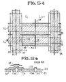
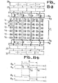
- FIG. 5a represents a top view and FIG. 5b a sectional view of an embodiment of a photosensitive dot matrix in which the grouping of the column connections illustrated in Figure 4a.
- FIG. 5a the grids 33, separated from each other by isolation barriers 51 produced as above. Between the grids 33 and the isolation barriers 51 are located the zones 38 in which are produced, in the variant shown, photodiodes.
- One of photosensitive points thus constituted is surrounded by a thick line and spotted 50 Figure 5a: it belongs to the L line. and in column Ci and the charges it stores are read to the left as represented by an arrow 56.
- the reading columns are grouped by two on either side of a vertical isolation barrier, also marked 51. There are therefore on each side of the isolation 51, two column diodes marked 35 and produced as above, for example in the substrate 21 (FIG. 5b).
- the screen grid is now marked 54 and covers both the isolation barrier 51 and the two reading diodes 35 which are located on either side of the barrier 51.
- the MOS capacitance grid 33 covers the substrate 21 and the screen grids 54, by means of an insulating layer.
- an opaque layer 32 is placed above the reading diodes 35; in the present case, a single layer 32 is deposited for the two reading diodes located on either side of the same barrier 51.
- FIG. 5b shows the case where photodiodes are produced in the zones 38 which also extend under the grid of MOS capacities 33, outside the zones occupied by the screen grids-54 and the isolation barriers 51.
- FIG. 6a represents a variant of the embodiment of FIG. 4a in which the double column is replaced by a single column, the isolation between the photosensitive points being carried out by independent screen grids.
- the photosensitive matrix 1 which comprises for example six rows (L 1 to L 6 ) and eight columns (C 1 to C 8 ), the colored filters being distributed in the same way as in FIG. 4a , and the two line memories 27 and 29 located on either side of the matrix 1, connected respectively to the two shift registers 37 and 39.
- the device here comprises two switching elements 67 and 69 interposed respectively before the line memories 27 and 29.
- the columns C 1 to C 8 that constitute the photosensitive dots are connected two by two to the same column connection (c 1 to c 4 in the figure), which comprises a reading diode 35, illustrated in FIG. 6a by a simple connection, surrounded by two screen grids on either side of the reading diode 35, these grids being marked 64 for the column C 1 and 74 for column C 2 .
- the screen grids such as 64 which correspond to the odd columns (C l , C 3 , C 5 ' C 7 ), are connected to a potential ⁇ G
- the screen grids such as 74 connected to the even columns (C 2 , C 4 , C 6 and C 8 ) are connected to a potential ⁇ D.
- the reading diodes 35 are connected, at each of their ends, to the memories 27 and 29 respectively by means of transistors 61 and 62, controlled respectively by potentials ⁇ B and ⁇ H , these transistors respectively constituting the switching devices 67 and 69.
- FIG. 6b represents the form of the control signals 0 B, ⁇ H , ⁇ G and ⁇ D used in the device of FIG. 6a, which are voltages varying between a high level and a low level.
- the signal ⁇ B is only high between time t 8 and time t 9 , t 9 -t 8 being slightly less than D / 2;
- the signal ⁇ H is in the high state only between an instant t 10 and the instant t 11 , with t 11 - t 10 slightly less than D / 2;
- the signals ⁇ G and ⁇ D respectively have the same form as the signals ⁇ B and ⁇ H.
- the operation of the device is as follows.
- the signals ⁇ B and ⁇ G returned to the low level while the signals ⁇ H and ⁇ D are at the high level and the operation is then inverse of the previous one, that is to say that this are the charges stored in the photosensitive points of the even columns which are discharged by the diode 35 and they are directed towards the line memory 29 exclusively via the transistors 62, the only conductors.
- Figure 7a shows a top view and Figure 7b a sectional view of an embodiment of a photosensitive matrix capable of being used in the device of Figure 6a.
- This structure differs from that of FIG. 5a only at the level of the charge collecting columns.
- the photosensitive point 50 constituted by an MOS capacitance produced by the grid 33, the semiconductor substrate 21 and the insulator 22, and a zone 38 in which a photodiode has been produced which extends for example also under the grid 33 , limited by the elements 51 and 74, as shown in the section of FIG. 7b, produced in the device of FIG. 7a along a line CC, at the photosensitive point 50 and the grid 33.
- the reading of this point is made from the left (arrow 56).
- the charge collection column is here constituted by a column diode 35 partially covered by the screen grid 64, the latter also extending above the substrate 21 to the left of the reading diode 35.
- the grid. screen 74 covers the other part of the diode 35, extends over a part of the substrate situated to the right of this diode and also extends, by means of an insulating layer, above the grid screen 64.
- the assembly is covered with the grid 33, above which the opaque layer 32 is still arranged by means of an insulating layer, at the level of the diode 35.
- the advantage of the structure as described in FIGS. 6 and 7 is the elimination of the insulation between two columns and, consequently, an increase in sensitivity. For example, this increase can reach 30% compared to a structure such as that of FIG. 3.
- the invention is not limited to the embodiments described above but encompasses all the variants which are within the reach of those skilled in the art. This is how the arrangement of the colored filters has been described with the three classic colors green, blue and red, but can of course be applied to the three complementary colors. previous ones, or to other sets of three colors, such as green, yellow and white or green, yellow and cyan for example.
Landscapes
- Engineering & Computer Science (AREA)
- Multimedia (AREA)
- Signal Processing (AREA)
- Physics & Mathematics (AREA)
- Spectroscopy & Molecular Physics (AREA)
- Solid State Image Pick-Up Elements (AREA)
- Color Television Image Signal Generators (AREA)
- Transforming Light Signals Into Electric Signals (AREA)
Applications Claiming Priority (2)
| Application Number | Priority Date | Filing Date | Title |
|---|---|---|---|
| FR8106432 | 1981-03-31 | ||
| FR8106432A FR2503502B1 (fr) | 1981-03-31 | 1981-03-31 | Dispositif d'analyse d'images en couleur utilisant le transfert de charges electriques et camera de television comportant un tel dispositif |
Publications (2)
| Publication Number | Publication Date |
|---|---|
| EP0063061A1 true EP0063061A1 (de) | 1982-10-20 |
| EP0063061B1 EP0063061B1 (de) | 1984-08-22 |
Family
ID=9256821
Family Applications (1)
| Application Number | Title | Priority Date | Filing Date |
|---|---|---|---|
| EP82400462A Expired EP0063061B1 (de) | 1981-03-31 | 1982-03-12 | Farbbildabtasteinrichtung unter Verwendung von elektrischer Ladungsübertragung und eine solche Einrichtung enthaltende Fernsehkamera |
Country Status (5)
| Country | Link |
|---|---|
| US (1) | US4453177A (de) |
| EP (1) | EP0063061B1 (de) |
| JP (1) | JPH0620315B2 (de) |
| DE (1) | DE3260595D1 (de) |
| FR (1) | FR2503502B1 (de) |
Cited By (6)
| Publication number | Priority date | Publication date | Assignee | Title |
|---|---|---|---|---|
| FR2533056A1 (fr) * | 1982-09-14 | 1984-03-16 | Thomson Csf | Imageur a transfert de lignes et camera de television comportant un tel imageur |
| GB2134347A (en) * | 1982-12-07 | 1984-08-08 | Canon Kk | Solid state image pick-up arrangement |
| FR2542919A1 (fr) * | 1983-03-18 | 1984-09-21 | Hitachi Ltd | Dispositif a l'etat solide de formation d'images en couleurs, comportant un filtre colore |
| FR2548505A1 (fr) * | 1983-06-30 | 1985-01-04 | Thomson Csf | Camera de television en couleur, a imageur solide a transfert de lignes |
| WO1990005424A1 (de) * | 1988-10-31 | 1990-05-17 | Reimar Lenz | Optoelektronischer farbbildwandler |
| US5877807A (en) * | 1988-10-31 | 1999-03-02 | Lenz; Reimar | Optoelectronic colored image converter |
Families Citing this family (20)
| Publication number | Priority date | Publication date | Assignee | Title |
|---|---|---|---|---|
| FR2522235B1 (fr) * | 1982-02-19 | 1986-02-21 | Thomson Brandt | Camera de television en couleurs comportant un filtre matriciel trichrome |
| FR2534435B1 (fr) * | 1982-10-08 | 1986-05-09 | Thomson Csf | Camera de television couleur monosenseur |
| DE3371454D1 (en) * | 1982-12-21 | 1987-06-11 | Thomson Csf | Method for scanning a line-transfer photosensitive device, and apparatus for carrying out the method |
| US4821088A (en) * | 1986-11-27 | 1989-04-11 | Fuji Photo Film Co., Ltd. | Solid-state color image pickup unit with mosaic color filter and two horizontal output registers |
| US4840725A (en) * | 1987-06-19 | 1989-06-20 | The Standard Oil Company | Conversion of high boiling liquid organic materials to lower boiling materials |
| JPS6454978A (en) * | 1987-08-26 | 1989-03-02 | Toshiba Corp | Solid-state image pickup element |
| JP2891550B2 (ja) * | 1991-01-11 | 1999-05-17 | 三菱電機株式会社 | イメージセンサ |
| DE4134666C2 (de) * | 1991-10-19 | 2002-03-28 | Zeiss Carl | Verfahren und Schaltung zur Verarbeitung optischer Signale |
| US5614950A (en) * | 1995-08-02 | 1997-03-25 | Lg Semicon Co., Ltd. | CCD image sensor and method of preventing a smear phenomenon in the sensor |
| JP3548410B2 (ja) | 1997-12-25 | 2004-07-28 | キヤノン株式会社 | 固体撮像装置および固体撮像装置の信号読み出し方法 |
| US7139025B1 (en) * | 1998-10-29 | 2006-11-21 | Micron Technology, Inc. | Active pixel sensor with mixed analog and digital signal integration |
| JP4532899B2 (ja) * | 2001-08-17 | 2010-08-25 | マイクロン テクノロジー, インク. | 列並列adcを有するcmosセンサにおける倍速化 |
| US7859581B2 (en) * | 2003-07-15 | 2010-12-28 | Eastman Kodak Company | Image sensor with charge binning and dual channel readout |
| JP4385844B2 (ja) * | 2004-04-23 | 2009-12-16 | ソニー株式会社 | 固体撮像装置および固体撮像装置の駆動方法 |
| JP2005333265A (ja) * | 2004-05-18 | 2005-12-02 | Olympus Corp | 固体撮像素子および装置 |
| JP4333478B2 (ja) * | 2004-05-27 | 2009-09-16 | 株式会社ニコン | 撮像装置および画像処理プログラム |
| JP4380439B2 (ja) * | 2004-07-16 | 2009-12-09 | ソニー株式会社 | データ処理方法およびデータ処理装置並びに物理量分布検知の半導体装置および電子機器 |
| JP4193768B2 (ja) * | 2004-07-16 | 2008-12-10 | ソニー株式会社 | データ処理方法並びに物理量分布検知の半導体装置および電子機器 |
| EP1971129A1 (de) * | 2007-03-16 | 2008-09-17 | STMicroelectronics (Research & Development) Limited | Verbesserungen bei oder im Zusammenhang mit Bildsensoren |
| JP5458690B2 (ja) * | 2009-06-22 | 2014-04-02 | ソニー株式会社 | 固体撮像装置およびカメラ |
Citations (7)
| Publication number | Priority date | Publication date | Assignee | Title |
|---|---|---|---|---|
| FR2314584A1 (fr) * | 1975-06-09 | 1977-01-07 | Philips Nv | Dispositif capteur d'images |
| US4016550A (en) * | 1975-11-24 | 1977-04-05 | Rca Corporation | Charge transfer readout of charge injection device arrays |
| US4047203A (en) * | 1976-05-12 | 1977-09-06 | Eastman Kodak Company | Color imaging array |
| FR2367353A1 (fr) * | 1976-10-06 | 1978-05-05 | Hitachi Ltd | Dispositif de formation d'image a semi-conducteur |
| FR2376517A1 (fr) * | 1976-12-30 | 1978-07-28 | Ibm | Structure photosensible a l'etat solide presentant une linearite de charge amelioree |
| GB2001504A (en) * | 1977-07-13 | 1979-01-31 | Hitachi Ltd | Colour solidstate imaging device |
| EP0038725A1 (de) * | 1980-04-23 | 1981-10-28 | Thomson-Csf | Photoempfindliche Vorrichtung, die durch Ladungsübertragung abgelesen wird, sowie eine Fernsehkamera, die eine solche Vorrichtung enthält |
Family Cites Families (3)
| Publication number | Priority date | Publication date | Assignee | Title |
|---|---|---|---|---|
| JPS5138826A (en) * | 1974-09-27 | 1976-03-31 | Matsushita Electric Industrial Co Ltd | Karaakotaisatsuzosochi |
| DE2838098A1 (de) * | 1978-08-31 | 1980-03-13 | Siemens Ag | Anordnung zur farbbildabtastung |
| JPS568968A (en) * | 1979-07-05 | 1981-01-29 | Matsushita Electric Ind Co Ltd | Solid-state image pickup unit |
-
1981
- 1981-03-31 FR FR8106432A patent/FR2503502B1/fr not_active Expired
-
1982
- 1982-03-12 EP EP82400462A patent/EP0063061B1/de not_active Expired
- 1982-03-12 DE DE8282400462T patent/DE3260595D1/de not_active Expired
- 1982-03-25 US US06/361,722 patent/US4453177A/en not_active Expired - Lifetime
- 1982-03-31 JP JP57053618A patent/JPH0620315B2/ja not_active Expired - Lifetime
Patent Citations (7)
| Publication number | Priority date | Publication date | Assignee | Title |
|---|---|---|---|---|
| FR2314584A1 (fr) * | 1975-06-09 | 1977-01-07 | Philips Nv | Dispositif capteur d'images |
| US4016550A (en) * | 1975-11-24 | 1977-04-05 | Rca Corporation | Charge transfer readout of charge injection device arrays |
| US4047203A (en) * | 1976-05-12 | 1977-09-06 | Eastman Kodak Company | Color imaging array |
| FR2367353A1 (fr) * | 1976-10-06 | 1978-05-05 | Hitachi Ltd | Dispositif de formation d'image a semi-conducteur |
| FR2376517A1 (fr) * | 1976-12-30 | 1978-07-28 | Ibm | Structure photosensible a l'etat solide presentant une linearite de charge amelioree |
| GB2001504A (en) * | 1977-07-13 | 1979-01-31 | Hitachi Ltd | Colour solidstate imaging device |
| EP0038725A1 (de) * | 1980-04-23 | 1981-10-28 | Thomson-Csf | Photoempfindliche Vorrichtung, die durch Ladungsübertragung abgelesen wird, sowie eine Fernsehkamera, die eine solche Vorrichtung enthält |
Cited By (6)
| Publication number | Priority date | Publication date | Assignee | Title |
|---|---|---|---|---|
| FR2533056A1 (fr) * | 1982-09-14 | 1984-03-16 | Thomson Csf | Imageur a transfert de lignes et camera de television comportant un tel imageur |
| GB2134347A (en) * | 1982-12-07 | 1984-08-08 | Canon Kk | Solid state image pick-up arrangement |
| FR2542919A1 (fr) * | 1983-03-18 | 1984-09-21 | Hitachi Ltd | Dispositif a l'etat solide de formation d'images en couleurs, comportant un filtre colore |
| FR2548505A1 (fr) * | 1983-06-30 | 1985-01-04 | Thomson Csf | Camera de television en couleur, a imageur solide a transfert de lignes |
| WO1990005424A1 (de) * | 1988-10-31 | 1990-05-17 | Reimar Lenz | Optoelektronischer farbbildwandler |
| US5877807A (en) * | 1988-10-31 | 1999-03-02 | Lenz; Reimar | Optoelectronic colored image converter |
Also Published As
| Publication number | Publication date |
|---|---|
| JPH0620315B2 (ja) | 1994-03-16 |
| JPS57176893A (en) | 1982-10-30 |
| US4453177A (en) | 1984-06-05 |
| EP0063061B1 (de) | 1984-08-22 |
| FR2503502B1 (fr) | 1985-07-05 |
| FR2503502A1 (fr) | 1982-10-08 |
| DE3260595D1 (en) | 1984-09-27 |
Similar Documents
| Publication | Publication Date | Title |
|---|---|---|
| EP0063061B1 (de) | Farbbildabtasteinrichtung unter Verwendung von elektrischer Ladungsübertragung und eine solche Einrichtung enthaltende Fernsehkamera | |
| EP0038725B1 (de) | Photoempfindliche Vorrichtung, die durch Ladungsübertragung abgelesen wird, sowie eine Fernsehkamera, die eine solche Vorrichtung enthält | |
| EP0064890B1 (de) | Einen Zeilenspeicher umfassende Einrichtung zur Bildabtastung in aufeinanderfolgenden Zeilen unter Verwendung elektrischer Ladungsübertragung und Fernsehkamera mit einer solchen Einrichtung | |
| FR3060250B1 (fr) | Capteur d'image pour capter une image en 2d et une profondeur | |
| FR2510852A1 (fr) | Matrice et dispositif de formation d'images en couleurs | |
| FR2537369A1 (fr) | Dispositif analyseur d'image a semi-conducteurs et systeme analyseur l'utilisant | |
| FR2496371A1 (fr) | Reseau de formation d'images en couleur et dispositif de formation d'images en couleur l'incorporant | |
| EP0145543B1 (de) | Ladungsgekoppelte mehrzeilige lineare Anordnung | |
| FR2556873A1 (fr) | Analyseur d'images a couplage de charges avec des registres cloisonnes pour les transferts de charges simultanes dans des directions opposees. | |
| EP2315251A1 (de) | Bildgeber mit vertikalem Transfergate und sein Herstellungsverfahren | |
| FR2652655A1 (fr) | Dispositif matriciel de grandes dimensions pour la prise ou la restitution d'images. | |
| EP0435773B1 (de) | Bildaufnahmeeinrichtung mit integrierten Ablenkschaltungen | |
| EP0060752B1 (de) | Zweidimensionale lichtempfindliche Festkörperanordnung und Ladungsübertragungsbildsensor, der eine solche Anordnung enthält | |
| FR2533056A1 (fr) | Imageur a transfert de lignes et camera de television comportant un tel imageur | |
| FR2509909A1 (fr) | Detecteur d'image a l'etat solide | |
| FR2470507A1 (fr) | Filtre de couleur | |
| EP0082035B1 (de) | Bildaufnahme und-ableseeinrichtung | |
| FR2867936A1 (fr) | Procede et capteur d'image pour effectuer un double sous-echantillonnage correle(cdss) de pixels dans une matrice de capteurs a pixels actifs (aps) | |
| EP1627432B1 (de) | Cmos bildaufnahmevorrichtung | |
| FR2504336A1 (fr) | Dispositif d'enregistrement de television pourvu d'un panneau d'enregistrement d'images a semi-conducteurs | |
| EP0207826B1 (de) | Detektorvorrichtung mit Zeitverzögerung und Integration in Phase | |
| FR2668303A1 (fr) | Capteur optique a faible diaphotie. | |
| FR2488085A1 (fr) | Dispositif de commutation pour la decharge d'une capacite, et camera de prise de vues comprenant ce dispositif | |
| EP4280283A1 (de) | Bildsensor | |
| JP2739601B2 (ja) | 撮像装置 |
Legal Events
| Date | Code | Title | Description |
|---|---|---|---|
| PUAI | Public reference made under article 153(3) epc to a published international application that has entered the european phase |
Free format text: ORIGINAL CODE: 0009012 |
|
| AK | Designated contracting states |
Designated state(s): DE FR GB NL |
|
| 17P | Request for examination filed |
Effective date: 19821030 |
|
| GRAA | (expected) grant |
Free format text: ORIGINAL CODE: 0009210 |
|
| AK | Designated contracting states |
Designated state(s): DE FR GB NL |
|
| REF | Corresponds to: |
Ref document number: 3260595 Country of ref document: DE Date of ref document: 19840927 |
|
| PLBE | No opposition filed within time limit |
Free format text: ORIGINAL CODE: 0009261 |
|
| STAA | Information on the status of an ep patent application or granted ep patent |
Free format text: STATUS: NO OPPOSITION FILED WITHIN TIME LIMIT |
|
| 26N | No opposition filed | ||
| REG | Reference to a national code |
Ref country code: FR Ref legal event code: CL |
|
| PGFP | Annual fee paid to national office [announced via postgrant information from national office to epo] |
Ref country code: DE Payment date: 20010214 Year of fee payment: 20 |
|
| PGFP | Annual fee paid to national office [announced via postgrant information from national office to epo] |
Ref country code: GB Payment date: 20010222 Year of fee payment: 20 |
|
| PGFP | Annual fee paid to national office [announced via postgrant information from national office to epo] |
Ref country code: NL Payment date: 20010315 Year of fee payment: 20 |
|
| PGFP | Annual fee paid to national office [announced via postgrant information from national office to epo] |
Ref country code: FR Payment date: 20010320 Year of fee payment: 20 |
|
| REG | Reference to a national code |
Ref country code: GB Ref legal event code: IF02 |
|
| PG25 | Lapsed in a contracting state [announced via postgrant information from national office to epo] |
Ref country code: GB Free format text: LAPSE BECAUSE OF EXPIRATION OF PROTECTION Effective date: 20020311 |
|
| PG25 | Lapsed in a contracting state [announced via postgrant information from national office to epo] |
Ref country code: NL Free format text: LAPSE BECAUSE OF EXPIRATION OF PROTECTION Effective date: 20020312 |
|
| REG | Reference to a national code |
Ref country code: GB Ref legal event code: PE20 Effective date: 20020311 |
|
| NLV7 | Nl: ceased due to reaching the maximum lifetime of a patent |
Effective date: 20020312 |