EP0063316A1 - Procédé et appareil de lecture d'information d'images - Google Patents
Procédé et appareil de lecture d'information d'images Download PDFInfo
- Publication number
- EP0063316A1 EP0063316A1 EP82102949A EP82102949A EP0063316A1 EP 0063316 A1 EP0063316 A1 EP 0063316A1 EP 82102949 A EP82102949 A EP 82102949A EP 82102949 A EP82102949 A EP 82102949A EP 0063316 A1 EP0063316 A1 EP 0063316A1
- Authority
- EP
- European Patent Office
- Prior art keywords
- integrator
- integration
- clock
- reset
- integrators
- Prior art date
- Legal status (The legal status is an assumption and is not a legal conclusion. Google has not performed a legal analysis and makes no representation as to the accuracy of the status listed.)
- Granted
Links
- 238000000034 method Methods 0.000 title claims description 16
- 230000010354 integration Effects 0.000 claims abstract description 118
- 230000001052 transient effect Effects 0.000 claims abstract description 10
- 238000005070 sampling Methods 0.000 claims description 51
- OAICVXFJPJFONN-UHFFFAOYSA-N Phosphorus Chemical compound [P] OAICVXFJPJFONN-UHFFFAOYSA-N 0.000 claims description 13
- 230000002411 adverse Effects 0.000 claims description 9
- 230000000694 effects Effects 0.000 claims description 4
- 230000003287 optical effect Effects 0.000 claims description 3
- 230000005855 radiation Effects 0.000 description 15
- 238000006243 chemical reaction Methods 0.000 description 11
- 230000004936 stimulating effect Effects 0.000 description 3
- 230000000638 stimulation Effects 0.000 description 3
- 101100166839 Arabidopsis thaliana CESA1 gene Proteins 0.000 description 2
- 101100449952 Arabidopsis thaliana KOR gene Proteins 0.000 description 2
- 230000008859 change Effects 0.000 description 2
- 238000003745 diagnosis Methods 0.000 description 2
- 230000008569 process Effects 0.000 description 2
- 241000143379 Idaea rufaria Species 0.000 description 1
- 238000013459 approach Methods 0.000 description 1
- 230000002238 attenuated effect Effects 0.000 description 1
- 239000003990 capacitor Substances 0.000 description 1
- 238000010276 construction Methods 0.000 description 1
- 238000007796 conventional method Methods 0.000 description 1
- 230000001934 delay Effects 0.000 description 1
- 230000003111 delayed effect Effects 0.000 description 1
- 238000001514 detection method Methods 0.000 description 1
- 238000010586 diagram Methods 0.000 description 1
- 238000007599 discharging Methods 0.000 description 1
- 230000006872 improvement Effects 0.000 description 1
- 238000002955 isolation Methods 0.000 description 1
- 230000004044 response Effects 0.000 description 1
- 230000001960 triggered effect Effects 0.000 description 1
Images

Classifications
-
- G—PHYSICS
- G11—INFORMATION STORAGE
- G11B—INFORMATION STORAGE BASED ON RELATIVE MOVEMENT BETWEEN RECORD CARRIER AND TRANSDUCER
- G11B7/00—Recording or reproducing by optical means, e.g. recording using a thermal beam of optical radiation by modifying optical properties or the physical structure, reproducing using an optical beam at lower power by sensing optical properties; Record carriers therefor
- G11B7/004—Recording, reproducing or erasing methods; Read, write or erase circuits therefor
- G11B7/005—Reproducing
-
- G—PHYSICS
- G02—OPTICS
- G02B—OPTICAL ELEMENTS, SYSTEMS OR APPARATUS
- G02B26/00—Optical devices or arrangements for the control of light using movable or deformable optical elements
- G02B26/08—Optical devices or arrangements for the control of light using movable or deformable optical elements for controlling the direction of light
- G02B26/10—Scanning systems
-
- G—PHYSICS
- G11—INFORMATION STORAGE
- G11B—INFORMATION STORAGE BASED ON RELATIVE MOVEMENT BETWEEN RECORD CARRIER AND TRANSDUCER
- G11B7/00—Recording or reproducing by optical means, e.g. recording using a thermal beam of optical radiation by modifying optical properties or the physical structure, reproducing using an optical beam at lower power by sensing optical properties; Record carriers therefor
- G11B7/002—Recording, reproducing or erasing systems characterised by the shape or form of the carrier
- G11B7/0025—Recording, reproducing or erasing systems characterised by the shape or form of the carrier with cylinders or cylinder-like carriers or cylindrical sections or flat carriers loaded onto a cylindrical surface, e.g. truncated cones
-
- H—ELECTRICITY
- H04—ELECTRIC COMMUNICATION TECHNIQUE
- H04N—PICTORIAL COMMUNICATION, e.g. TELEVISION
- H04N1/00—Scanning, transmission or reproduction of documents or the like, e.g. facsimile transmission; Details thereof
- H04N1/40—Picture signal circuits
Definitions
- This invention relates to a method of reading out image information stored on a recording medium, in which the image information is optically scanned in two directions, the resulting emitted, transmitted or reflected light is detected and converted to an electric output signal, the output signal is then integrated for a predetermined time and subjected to a sampling process, and a picture element of the image information is read out as a sampled- value train, and an apparatus for carrying out the method.
- This invention is particularly related to a method of and apparatus for reading out image information, which can effectively convert a detected.light even of a low intensity to an image signal.
- Techniques for detecting a weak light and reading image information are required for example in the fields of medical image processing, radiation image processing, nuclear electronics, facsimile, printing plate making by use of a laser beam, or the like.
- signals are generally passed through a low-pass.filter or an integration circuit before processing in order to convert the weak light to an electric signal at as high efficiency as possible.
- a stimulable phosphor as an intermediate medium for radiation image recording for the purpose of improving the efficiency and accuracy of medical diagnosis.
- S/N ratio signal-to- noise ratio
- the above-mentioned radiation image read-out system using a stimulable phosphor as an intermediate recording medium is disclosed for example in Japanese Unexamined Patent Publication No. 11395/1981 and U.S. Patent Nos. 4,258,264 and 4,284,889.
- the stimulable phosphor is exposed through a human body to a radiation to have a radiation image stored thereon, the stimulable phosphor is then scanned at a high speed with a stimulating ray to cause it to emit light therefrom in the pattern of the .stored image, and the-light emitted from the stimulable phosphor upon stimulation thereof is photoelectrically detected and converted to an electric signal.
- the obtained electric signal is processed as desired to reproduce a visible image having an image quality suitable for viewing and diagnosis purposes.
- an optical system which can effectively guide the detected light to the photoelectric conversion system is adopted and, in addition, a low-pass filter and an integration circuit are used to improve the use efficiency of the photoelectrically converted information.
- the low-pass filter works on the basis of the time constant of a capacitor-resistor and, consequently, presents a very real problem with regard to a signal sampling process. Namely, signal samples cannot be completely separated from each other, so that a preceding .sample adversely affects the subsequent sampling output signal. Further, the use efficiency of light information is low because of low integration efficiency.
- the integrator As for the integration circuit, it is essential that the integrator be reset to prepare for the next sampling. Accordingly, the electric signal corresponding to light information which is input during the resetting period cannot be integrated. More specifically, in order to sequentially integrate the input signal for a predetermined period and determine and sample the mean value or the total value of the integrated signal, it is necessary that the integrator be reset to the initial state each time the predetermined integration period runs out. However, it takes 1 to 2ps for even the most rapid switch presently available to be reset. A resetting period of this order greatly interferes with desired high-speed sampling. Thus the integration efficiency in the sampling region is low and it is impossible to improve the S/N ratio.
- the primary object of the present invention is to provide a method of and apparatus for reading out image information, which can photoelectrically convert light information at a high S/N ratio to provide a reproduced image of a high quality.
- Another object of the present invention is to provide a method of and apparatus for reading out image information, which can optimize utilization of the photoelectrically converted image signal which is input to the integrator.
- the specific object of the present invention is to provide a method of and apparatus for reading out image information, which car read image, information by carrying out signal conversion at any sampling frequency up to a high-frequency up to that determined by the changeover transient time intrinsic to the integrator.
- the above objects are accomplished by using a plurality of integrators, sequentially switching the integrators to start integration each time the first clock pulse determining the size of the picture element is input, setting the integration periods of the integrators to a value not shorter than one clock length of the first clock pulse so as to partially overlap each other, actuating the sampling of the signal from the started integrator by the second clock pulse at a point of time within the overlap region of the integration periods but outside the regions where the next integrator is in the switching transient state to integration start mode and where said started integrator is reset, and determining the reset state holding period of each integrator so that each integrator is sufficiently reset to prepare for the start of the next integration.
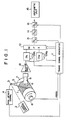
- FIG. 1 shows an embodiment of the radiation image read-out apparatus in accordance with the present invention.
- a radiation image stored on a stimulable phosphor sheet 1 is scanned in two directions with a stimulating ray 5 from a laser source 2 via a scanning mirror 3.
- the stimulable phosphor sheet 1 is driven by a rotating drum 7.
- Light 6 emitted from the stimulable phosphor sheet 1 upon stimulation thereof is guided to a photodetector 9 by a light collecting means (not shown) capable of effectively collecting light.
- the emitted light 6 is photoelectrically converted to time-series electric image signal corresponding to the amount of radiation energy-stored on the stimulable phosphor sheet 1.
- the electric output signal obtained from the photodetector 9 contains the random noise of the emitted light 6 and is input to two parallel-connected integrators IN1 and IN2 via a buffer amplifier 10.
- the integrators IN1 and IN2 are provided with reset switches SW1 and SW2, respectively.
- timing signal generating means 11 receives the signal input from a rotation angle detecting rotary encoder 8 engaged with the cylindrical rotating drum 7 which holds the stimulable phosphor sheet 1 thereon and moves it in the sub-scanning direction for read out.
- the timing signal generating means 11 is also fed with a signal input from a position detecting signal generating means 4 which detects the position of the stimulating ray 5. Based on these input signals, the timing signal generating means 11 generates output signals for controlling the changeover of the reset switches SW1 and SW2 for the integrators INl and IN2-, respectively, and other necessary timing signals.
- the output ends of the integrators IN1 and IN2 are connected with an analog multiplexer 12 which collects data by quickly sampling the integration output signals for respective picture elements, followed by a sample holding circuit 13, an analog signal processing amplifier 14 and an analog-to-digital converter (A/D converter) 15. Digital image signals converted and extracted by these circuits are then sent to an arithmetic processing unit 16 via a memory device such as magnetic tape for the purpose of processing the data so as to obtain a radiation image permitting high diagnostic efficiency and accuracy. In this way, the digital signals are converted to desired image signals by the arithmetic processing unit 16 and used for the reproduction of radiation image information.
- a photomultiplier is used as the photodetector 9.
- the above-mentioned timing signal generating means 11 has various components described below. First, it has a circuit for generating and supplying a first clock pulse, i.e. an integration start clock, which alternately switches the integrators IN1 and IN2 having the reset switches SW1 and SW2, respectively, from reset state (reset holding mode) to integration holding state (integration mode) in synchronization with clock timing of a predetermined picture element resolving frequency. Second, the timing signal generating means 11 has a circuit for setting the integration mode holding time which sets the integration times of the integrators IN1 and IN2, respectively, to values not less than the one clock length of the above-mentioned integration start clock.
- a first clock pulse i.e. an integration start clock
- the generaling means 11 is also provided with a circuit for generating and supplying a reset signal to each of the integrators IN1 and IN2 at the ends of their integration mode holding times, and a sampling timing setting circuit capable of timing the signal sampling from each integrator to a desired point of time within the integration time extending from the end of one clock length of the above-mentioned integration start clock to the start of the other integrator.
- the timing signal generating means 11 also has a circuit for generating and supplying a second clock pulse (sampling command clock) to sample the integrator outputs in accordance with the timing set by the aforesaid sampling timing setting circuit.
- the sampling clock frequency is divided in half by a 1/2 frequency divider.
- a signal for starting the integrator INl is generated when the frequency-divided wave rises, and that for starting the integrator IN2 is generated when the frequency-divided wave falls.
- the timing signal generating means 11 in Figure 1 also embraces other necessary circuits such as a reference clock generator, and circuits for generating signals for timing the sample hold control, multiplexer control and A/D conversion control based on the reference clock pulse, rotary encoder output and position detection signal.
- the above-described one-shot-multivibrators alternately switch the integrators IN1 and IN2 in such a manner that their integration mode holding periods overlap each other for a predetermined time.
- the one-shot-multivibrators also send a sampling command with a predetermined time lag with respect to the integration start clock, and appropriately output timing signals for the analog multiplexer, sample holding and A/D conversion.
- Integration outputs obtained from the integrators IN1 and IN2 are selectively picked up from the analog multiplexer 12, held as samples and A/D converted in an appropriately timed manner.
- the analog signal processing amplifier 14 in Figure 1 conducts log-conversion, gamma (y) conversion, nonlinear conversion or the like as required when the read image signal is reproduced into the final image on a photographic film or a cathode ray tube.
- Figure 2 is a timing chart showing the sampling operations of the embodiment shown in Figure 1.
- reference character A designates the signal waveform detected by the photoelectric converter 9 and containing random noise
- B designates the first clock having a reference frequency.
- the frequency of the first clock B is divided in half to obtain a wave X.
- the integrator IN1 is started when the wave X rises, and integrator IN2 is started when it falls.
- Reference character S designates the second clock, i.e. the sampling command clock.
- Waves Cl, Dl and C2, D2 are output from four one-shot-multivibrators built in the timing signal generating means 11.
- the 0 state of waves Cl and C2 corresponds to the integration mode holding periods of the integrators IN1 and IN2, while the 1 state thereof corresponds to the integration reset periods.
- Dotted waves RSW1 and RSW2 respectively superposed on waves Cl and C2 indicate the resistance values of the reset switches SW1 and SW2, respectively.
- the waves RSW1 and RSW2 when the waves Cl and C2 are changed over to the integration start command mode, the resistance values of the integrator reset switches do not instantly change from zero to the infinity ( ⁇ ).
- waves Cl and C2 are switched from the 0 state to the 1 state and the integrators INl and IN2 receive the reset state holding command, the resistances of the integrator reset switches gradually change from the infinity to zero.
- Waves Dl and D2 generate the sampling clocks to issue the commands for sampling the outputs of the integrators IN1 and IN2 when the respective waves rise from 0 to 1.
- Reference characters El and E2 respectively designate the waves of the integration outputs obtained from the integrators IN1 and IN2 having the reset switches.
- the black dots in Figure 2 denote two sampling points corresponding to the rises of the one-shot-multivibrator output pulses Dl and D2.
- Reference characters tl and tl' each designate pulse widths of the one-shot-multivibrator outputs which determine the points of time for sampling the outputs of the integrators IN1 and IN2, respectively, and t2 and t2' denote pulse widths of the outputs of the one-shot-multivibrators which determine the integration mode holding times of the integrators IN1 and IN2, respectively.
- Pulse widths t3 and t3' denote the reset state holding times of the integrators IN1. and IN2, respectively.
- Reference characters T and T ' designate delays between the aforesaid first integration start clock and the second sampling clock, and toff and t'off designate the switching transient times elapsing from when the integrators IN1 and IN2 having reset switches receive the integration start signal to when their reset switches open to start integration.
- Switching transient times t on and t' on denote the times required for the reset switches to close and start integration after the integrators IN1 and IN2 having reset switches receive the integration reset signal.
- the outputs Cl and Dl (for controlling the integrator IN1) of the two one-shot-multivibrators started when the output wave X from the frequency dividing circuit rises are switched from 1 to 0 so as to form square pulse output waves whose pulse widths are set to-t2 and tl respectively by the predetermined time constants, and then return to the 1 state.
- the multivibrator output Cl is set to 0
- the reset switch SW1 of the integrator IN1 is opened and holds its open state.
- the reset switch SW1 is closed.
- the second clock pulse S2 is sent to sample the integration output of the integrator IN1.
- the second clock pulse S2 for sampling is generated tl after the first clock Bl is input, and the sampling timing is set to satisfy the condition where Namely, the integration output is sampled from the integrator IN1 at a point of time delayed by T from the clock B2 next to the first clock Bl which starts the integrator IN1. Because sampling of the output of the integrator IN1 is conducted under these conditions, the integrator IN1 can accomplish stable integration of the signal which is input thereto during the transient state period (t' off ) of the integrator IN2 switched to the integration mode at the point of time of the clock B2. Further, sampling of the output of the integrator IN1 occurs before it is reset at the end of its integration mode holding period t2.
- the integrator IN1 After the integration output of the integrator IN1 is sampled at S2, integration of the input signal A is conducted by the second integrator IN2 which has been stabilized in the integration mode by the first clock B2. Accordingly, the result of integration is not affected by spike-like noise occurring when the integrator IN1 is reset. Thereafter, the integrator IN1 is sufficiently reset to the original state and can get ready for the integration because its reset mode holding time t3 is longer than ton + t c where t c designates the time constant for discharging the charges integrated and accumulated by the integrator IN1. In the embodiment described herein, one cycle time of the integrator IN1, i.e.
- the value T may be set so that the time T - t'off is somewhat long within the range of T + t0 ⁇ t2. However, it should not be set in such a way that the time T - t'off is excessively long and double integration of the same input signal A simultaneously conducted by both integrators IN1 and IN2 during that time adversely affects the isolation between sample values and quality of the reproduced image.
- the waves C2 and D2 of the two multivibrators for the integrator IN2 are switched from the 1 state to the 0 state by the trigger signal generated when the frequency divider output wave X falls.
- the waves C2 and D2 form square wave pulse outputs having the predetermined pulse widths t2' (corresponding to the integration mode holding time of the integrator IN2) and tl' (corresponding to the setting time of integration output sampling timing of the integrator IN2) in the same manner as waves Cl and Dl for the integrator INl.
- the waves C2 and D2 return to the 1 state.
- the reset switch SW2 of the integrator IN2 is opened t'off after the clock B2 is input thereto and maintains the integrator IN2 in the integration state for the time t2'.
- the setting time t2' and reset period t3' of the multivibrator C2 and the setting time tl' of multivibrator D2 are set in the same manner as those for the integrator IN1.
- the time tl' elapsing from when the clock B2 is input to when the integration output of the integrator IN2 is sampled is set to satisfy the condition
- the integration mode holding time t2' for the. integrator IN2 is set to satisfy the condition
- the time tl is set equally to tl', and the time T to T '. However, they may be varied as desired provided that they satisfy the above-described conditions.
- the first integration start clocks Bl and B2 are input to the integrators IN1 and IN2, and the signal A which is input between the time T ' after Bl and the time T ' after B3 is sequentially integrated by the two integrators which are actuated alternately.
- the respective integration outputs are sampled at S2 and S3 to yield two sampled values.
- the output wave of integration conducted by the integrator IN2 is shown by E2.
- the integrator INl is held in the reset state and waits for the next integration start command.
- the integrator IN1 completes its one operation cycle and is switched to the integration mode holding state of the second cycle.
- the command clock S3 is generated to sample the output of the currently operating integrator IN2 at an appropriate point of time T ' after the clock B3, namely at a time after the opening transient interval toff of the reset switch SW1 runs out.
- the integrator IN2. is maintained in the reset condition for a sufficiently long period t3' and waits for the next integration start clock B4.
- the clock B 3 simultaneously actuates the multivibrators Cl and Dl of the integrator INl, and thereafter the multivibrator Dl outputs a command clock S4 to sample the integration output of the integrator INl when the predetermined time tl elapses after the clock B3 is input thereto.
- the first clock is generated at B4 to switch the integrator IN2 to the integration mode holding period of the next cycle and activate the multivibrator D2 which times the sampling command S5 for sampling the integration output of the integrator IN2.
- the sampling command S4 for the integrator TN1 is generated T after the clock B4 is input thereto, and soon the integrator IN1 is switched to the reset holding mode and waits for the next clock B5. In this way, the above-described operations are repeated.
- two or more integrators are activated alternately.
- the input signal supplied during the integration start transient period and the reset period of one integrator is input to the other integrator.
- the integration output of each integrator is sampled after the integration start transient period of the other integrator, which is activated for integration by a pulse issued one clock after the former integrator is actuated for integration, but before the former integrator to be sampled is reset. Accordingly, the integration output can be sampled in such a way that the integration efficiency for a continuously input signal is nearly 100% for any picture element resolving frequency 1/t0 within the range below the high-frequency region where the value t0 ( > t off ) approaches t off . In addition, it is possible to minimize the adverse effect of noise contained in the input signal.
- the reset periods t3 and t3' are preferably selected to satisfy the condition t3 (t3') > t on (t' on ) + 7CR wherein C denotes the integrating capacitor capacity of each integrator, and R denotes the reset switch on resistance, because in this case the residual electric charges can be attenuated to a level of about a quarter or below so as to prepare for the next integration.
- one-shot-multivibrators are used as the integrator mode control and sampling pulse control circuits.
- these circuits may be constructed for example by a means in which a square wave pulse having a duty factor of 50% is generated from the aforesaid first reference clock, the integration time is set equally to a 1.5 clock length (from the rise of pulse to the fall after the next), and integration is reset with the remaining 0.5 clock length (from the fall to the rise of pulse).
- the circuitry from the multiplexer to the A/D conversion in the above-mentioned embodiment may be replaced for example by an A/D conversion control system using a special computer.
- the number n of integrators may be set to any integer within the range satisfying the above-described conditions. However, the number n should be minimized to simplify the circuitry construction.
- N denotes the number of light quanta. Therefore .
- e the integration efficiency.
- the sampling frequency is generally within the range of from 10 to 500 kHz.
- the response delay time of the reset switch of the integrator is 2 ⁇ s, the integration efficiency e is Therefore, the S/N ratio is improved by a factor within the range of 5% to 50% in accordance with the present invention.
- signals are sampled without being adversely affected by spike-like noise occurring in the integration output due to the floating capacity of the reset switch when it is closed at the end of the integration mode. This eliminates the necessity of using and adjusting circuitry for absorbing and preventing the floating capacity of the reset switch in synchronization with the switching, and greatly improves the productivity of the radiation image read-out apparatus.
- the present invention makes it possible to accomplish signal.conversion at a high S/N ratio and effectively read out the image information contained in the signal detected from the image recording medium by minimizing the adverse effect of random noise contained in the detected signal, if any, and by eliminating spike-like noise occurring due to switching of the reset switches.
Landscapes
- Physics & Mathematics (AREA)
- General Physics & Mathematics (AREA)
- Optics & Photonics (AREA)
- Engineering & Computer Science (AREA)
- Multimedia (AREA)
- Signal Processing (AREA)
- Facsimile Scanning Arrangements (AREA)
- Transforming Light Signals Into Electric Signals (AREA)
- Image Input (AREA)
Applications Claiming Priority (2)
| Application Number | Priority Date | Filing Date | Title |
|---|---|---|---|
| JP52685/81 | 1981-04-08 | ||
| JP56052685A JPS57168579A (en) | 1981-04-08 | 1981-04-08 | Method and device for reading of picture information |
Publications (2)
| Publication Number | Publication Date |
|---|---|
| EP0063316A1 true EP0063316A1 (fr) | 1982-10-27 |
| EP0063316B1 EP0063316B1 (fr) | 1986-03-05 |
Family
ID=12921736
Family Applications (1)
| Application Number | Title | Priority Date | Filing Date |
|---|---|---|---|
| EP82102949A Expired EP0063316B1 (fr) | 1981-04-08 | 1982-04-06 | Procédé et appareil de lecture d'information d'images |
Country Status (4)
| Country | Link |
|---|---|
| US (1) | US4446487A (fr) |
| EP (1) | EP0063316B1 (fr) |
| JP (1) | JPS57168579A (fr) |
| DE (2) | DE63316T1 (fr) |
Cited By (1)
| Publication number | Priority date | Publication date | Assignee | Title |
|---|---|---|---|---|
| EP0776473A4 (fr) * | 1995-06-19 | 1998-05-20 | Denoptix Inc | Systeme rotatif d'exploration de plaques radiosensibles multicouches |
Families Citing this family (6)
| Publication number | Priority date | Publication date | Assignee | Title |
|---|---|---|---|---|
| JPS5979674A (ja) * | 1982-10-28 | 1984-05-08 | Toshiba Corp | カラ−密着センサ |
| JPS5983149A (ja) * | 1982-11-04 | 1984-05-14 | Fuji Photo Film Co Ltd | 階調補正曲線の作成方法 |
| US4599640A (en) * | 1984-02-29 | 1986-07-08 | Rca Corporation | Television camera with multiplexed A-D converter |
| WO2000033057A1 (fr) | 1998-11-25 | 2000-06-08 | Phormax Corporation | Dispositifs de balayage a double tete pour ecrans fluorescents |
| JP2002296714A (ja) * | 2001-03-30 | 2002-10-09 | Fuji Photo Film Co Ltd | 放射線画像情報読取方法 |
| WO2004102627A2 (fr) * | 2003-05-08 | 2004-11-25 | Alara, Inc. | Procede et dispositif pour effacement d'images radiographiques |
Citations (6)
| Publication number | Priority date | Publication date | Assignee | Title |
|---|---|---|---|---|
| US3524020A (en) * | 1968-03-28 | 1970-08-11 | Us Air Force | Apparatus for opto-electronic photographic image translation |
| GB1394572A (en) * | 1971-11-22 | 1975-05-21 | Secr Defence | Facsimile scanning apparatus |
| GB1400471A (en) * | 1971-09-03 | 1975-07-16 | Matsushita Electric Industrial Co Ltd | Apparatus for automatic computation of cardiothoracic ratio |
| FR2438856A1 (fr) * | 1978-10-05 | 1980-05-09 | Fuji Photo Film Co Ltd | Procede d'enregistrement d'une image de radiations |
| FR2450471A1 (fr) * | 1979-02-28 | 1980-09-26 | Fuji Photo Film Co Ltd | Procede de traitement par gradation et appareil pour systeme d'enregistrement d'image par rayonnement |
| US4258264A (en) * | 1978-07-12 | 1981-03-24 | Fuji Photo Film Co., Ltd. | Method of and apparatus for reading out a radiation image recorded in a stimulable phosphor |
Family Cites Families (2)
| Publication number | Priority date | Publication date | Assignee | Title |
|---|---|---|---|---|
| US4148061A (en) * | 1972-05-18 | 1979-04-03 | Lemelson Jerome H | Scanning apparatus and method |
| JPS5842514B2 (ja) * | 1975-03-31 | 1983-09-20 | 株式会社日立製作所 | エイゾウシンゴウホセイソウチ |
-
1981
- 1981-04-08 JP JP56052685A patent/JPS57168579A/ja active Granted
-
1982
- 1982-04-05 US US06/365,304 patent/US4446487A/en not_active Expired - Lifetime
- 1982-04-06 DE DE198282102949T patent/DE63316T1/de active Pending
- 1982-04-06 EP EP82102949A patent/EP0063316B1/fr not_active Expired
- 1982-04-06 DE DE8282102949T patent/DE3269554D1/de not_active Expired
Patent Citations (6)
| Publication number | Priority date | Publication date | Assignee | Title |
|---|---|---|---|---|
| US3524020A (en) * | 1968-03-28 | 1970-08-11 | Us Air Force | Apparatus for opto-electronic photographic image translation |
| GB1400471A (en) * | 1971-09-03 | 1975-07-16 | Matsushita Electric Industrial Co Ltd | Apparatus for automatic computation of cardiothoracic ratio |
| GB1394572A (en) * | 1971-11-22 | 1975-05-21 | Secr Defence | Facsimile scanning apparatus |
| US4258264A (en) * | 1978-07-12 | 1981-03-24 | Fuji Photo Film Co., Ltd. | Method of and apparatus for reading out a radiation image recorded in a stimulable phosphor |
| FR2438856A1 (fr) * | 1978-10-05 | 1980-05-09 | Fuji Photo Film Co Ltd | Procede d'enregistrement d'une image de radiations |
| FR2450471A1 (fr) * | 1979-02-28 | 1980-09-26 | Fuji Photo Film Co Ltd | Procede de traitement par gradation et appareil pour systeme d'enregistrement d'image par rayonnement |
Cited By (2)
| Publication number | Priority date | Publication date | Assignee | Title |
|---|---|---|---|---|
| EP0776473A4 (fr) * | 1995-06-19 | 1998-05-20 | Denoptix Inc | Systeme rotatif d'exploration de plaques radiosensibles multicouches |
| EP0987542A3 (fr) * | 1995-06-19 | 2001-03-14 | Alara, Inc. | Système rotatif d'exploration d'une pluralité de plaques radiosensibles |
Also Published As
| Publication number | Publication date |
|---|---|
| US4446487A (en) | 1984-05-01 |
| JPS57168579A (en) | 1982-10-16 |
| EP0063316B1 (fr) | 1986-03-05 |
| JPS6159590B2 (fr) | 1986-12-17 |
| DE3269554D1 (en) | 1986-04-10 |
| DE63316T1 (de) | 1983-04-14 |
Similar Documents
| Publication | Publication Date | Title |
|---|---|---|
| US4484073A (en) | Method of and apparatus for reading out radiation image information | |
| US4472744A (en) | Photoelectric converter apparatus | |
| EP0195270B1 (fr) | Caméra vidéo | |
| JP2566694B2 (ja) | 対象画像のスペクトル成分を捕獲するためのシステム | |
| EP0108308A2 (fr) | Appareil de conversion photo-électrique | |
| US4446487A (en) | Method of and apparatus for reading out image information | |
| GB2159016A (en) | Image data correction | |
| US5955725A (en) | Digitizing CCD array system | |
| US4252425A (en) | Camera focus detecting device | |
| JPH0391734A (ja) | 放射線画像読取装置 | |
| US4703177A (en) | Arrangement for the production of X-ray pictures by computer radiography | |
| US4742230A (en) | X-ray image detecting apparatus | |
| EP0594070B1 (fr) | Réduction de bruit dans un système de saisie de données avec matériau luminescent | |
| WO1996016510A1 (fr) | Appareil de prise d'images | |
| JP2571644B2 (ja) | イメージセンサ | |
| JPH01134619A (ja) | アナログーディジタル変換回路 | |
| SU1352435A1 (ru) | Устройство регистрации | |
| JP3046170B2 (ja) | Ccdラインセンサ駆動装置 | |
| SU1574014A1 (ru) | Многоканальный флуориметр | |
| EP0181031B1 (fr) | Optimisation de l'illumination de polarisation d'un vidicon | |
| SU1277952A1 (ru) | Сканирующее устройство | |
| SU561979A1 (ru) | Устройство дл считывани графической информации | |
| SU1626451A2 (ru) | Устройство дл автоматической фокусировки луча электронно-лучевой трубки | |
| JPS62116062A (ja) | 読取装置 | |
| SU966710A1 (ru) | Устройство дл считывани и селекции изображений объектов |
Legal Events
| Date | Code | Title | Description |
|---|---|---|---|
| PUAI | Public reference made under article 153(3) epc to a published international application that has entered the european phase |
Free format text: ORIGINAL CODE: 0009012 |
|
| AK | Designated contracting states |
Designated state(s): BE DE FR GB NL |
|
| TCNL | Nl: translation of patent claims filed | ||
| EL | Fr: translation of claims filed | ||
| DET | De: translation of patent claims | ||
| 17P | Request for examination filed |
Effective date: 19830218 |
|
| GRAA | (expected) grant |
Free format text: ORIGINAL CODE: 0009210 |
|
| AK | Designated contracting states |
Kind code of ref document: B1 Designated state(s): BE DE FR GB NL |
|
| REF | Corresponds to: |
Ref document number: 3269554 Country of ref document: DE Date of ref document: 19860410 |
|
| ET | Fr: translation filed | ||
| PLBE | No opposition filed within time limit |
Free format text: ORIGINAL CODE: 0009261 |
|
| STAA | Information on the status of an ep patent application or granted ep patent |
Free format text: STATUS: NO OPPOSITION FILED WITHIN TIME LIMIT |
|
| 26N | No opposition filed | ||
| PGFP | Annual fee paid to national office [announced via postgrant information from national office to epo] |
Ref country code: GB Payment date: 19960318 Year of fee payment: 15 Ref country code: FR Payment date: 19960318 Year of fee payment: 15 |
|
| PGFP | Annual fee paid to national office [announced via postgrant information from national office to epo] |
Ref country code: BE Payment date: 19960422 Year of fee payment: 15 |
|
| PGFP | Annual fee paid to national office [announced via postgrant information from national office to epo] |
Ref country code: NL Payment date: 19960430 Year of fee payment: 15 |
|
| PGFP | Annual fee paid to national office [announced via postgrant information from national office to epo] |
Ref country code: DE Payment date: 19960627 Year of fee payment: 15 |
|
| PG25 | Lapsed in a contracting state [announced via postgrant information from national office to epo] |
Ref country code: GB Effective date: 19970406 |
|
| PG25 | Lapsed in a contracting state [announced via postgrant information from national office to epo] |
Ref country code: BE Effective date: 19970430 |
|
| BERE | Be: lapsed |
Owner name: FUJI PHOTO FILM CO. LTD. Effective date: 19970430 |
|
| PG25 | Lapsed in a contracting state [announced via postgrant information from national office to epo] |
Ref country code: NL Effective date: 19971101 |
|
| GBPC | Gb: european patent ceased through non-payment of renewal fee |
Effective date: 19970406 |
|
| PG25 | Lapsed in a contracting state [announced via postgrant information from national office to epo] |
Ref country code: FR Free format text: LAPSE BECAUSE OF NON-PAYMENT OF DUE FEES Effective date: 19971231 |
|
| PG25 | Lapsed in a contracting state [announced via postgrant information from national office to epo] |
Ref country code: DE Free format text: LAPSE BECAUSE OF NON-PAYMENT OF DUE FEES Effective date: 19980101 |
|
| NLV4 | Nl: lapsed or anulled due to non-payment of the annual fee |
Effective date: 19971101 |
|
| REG | Reference to a national code |
Ref country code: FR Ref legal event code: ST |