EP0063429B1 - Appareil de lithographie par matrice de faisceaux d'électrons et méthode pour son utilisation - Google Patents
Appareil de lithographie par matrice de faisceaux d'électrons et méthode pour son utilisation Download PDFInfo
- Publication number
- EP0063429B1 EP0063429B1 EP82301670A EP82301670A EP0063429B1 EP 0063429 B1 EP0063429 B1 EP 0063429B1 EP 82301670 A EP82301670 A EP 82301670A EP 82301670 A EP82301670 A EP 82301670A EP 0063429 B1 EP0063429 B1 EP 0063429B1
- Authority
- EP
- European Patent Office
- Prior art keywords
- lenslet
- electron beam
- grid
- array
- chip
- Prior art date
- Legal status (The legal status is an assumption and is not a legal conclusion. Google has not performed a legal analysis and makes no representation as to the accuracy of the status listed.)
- Expired
Links
- 238000010894 electron beam technology Methods 0.000 title claims description 150
- 238000000034 method Methods 0.000 title claims description 54
- 238000001459 lithography Methods 0.000 title claims description 13
- 230000003287 optical effect Effects 0.000 claims description 45
- 239000004065 semiconductor Substances 0.000 claims description 33
- 238000013507 mapping Methods 0.000 claims description 25
- 230000015654 memory Effects 0.000 claims description 22
- 230000000694 effects Effects 0.000 claims description 17
- 238000012937 correction Methods 0.000 claims description 15
- 238000006073 displacement reaction Methods 0.000 claims description 14
- 238000010276 construction Methods 0.000 claims description 12
- 238000012545 processing Methods 0.000 claims description 12
- 230000001419 dependent effect Effects 0.000 claims description 11
- 238000005259 measurement Methods 0.000 claims description 10
- 238000000609 electron-beam lithography Methods 0.000 claims description 8
- 238000013519 translation Methods 0.000 claims description 7
- 238000003780 insertion Methods 0.000 claims description 6
- 238000005094 computer simulation Methods 0.000 claims description 5
- 230000037431 insertion Effects 0.000 claims description 5
- 230000009466 transformation Effects 0.000 claims description 4
- 241000226585 Antennaria plantaginifolia Species 0.000 claims description 3
- 238000013461 design Methods 0.000 claims description 3
- 230000017105 transposition Effects 0.000 claims description 2
- 230000001131 transforming effect Effects 0.000 claims 4
- 230000005284 excitation Effects 0.000 claims 2
- 230000014509 gene expression Effects 0.000 claims 1
- 238000007493 shaping process Methods 0.000 claims 1
- 235000012431 wafers Nutrition 0.000 description 56
- 230000007246 mechanism Effects 0.000 description 8
- 238000004519 manufacturing process Methods 0.000 description 7
- 239000000463 material Substances 0.000 description 7
- XUIMIQQOPSSXEZ-UHFFFAOYSA-N Silicon Chemical compound [Si] XUIMIQQOPSSXEZ-UHFFFAOYSA-N 0.000 description 4
- 229910052710 silicon Inorganic materials 0.000 description 4
- 239000010703 silicon Substances 0.000 description 4
- 238000003491 array Methods 0.000 description 3
- 238000010586 diagram Methods 0.000 description 3
- 230000006870 function Effects 0.000 description 3
- PCTMTFRHKVHKIS-BMFZQQSSSA-N (1s,3r,4e,6e,8e,10e,12e,14e,16e,18s,19r,20r,21s,25r,27r,30r,31r,33s,35r,37s,38r)-3-[(2r,3s,4s,5s,6r)-4-amino-3,5-dihydroxy-6-methyloxan-2-yl]oxy-19,25,27,30,31,33,35,37-octahydroxy-18,20,21-trimethyl-23-oxo-22,39-dioxabicyclo[33.3.1]nonatriaconta-4,6,8,10 Chemical compound C1C=C2C[C@@H](OS(O)(=O)=O)CC[C@]2(C)[C@@H]2[C@@H]1[C@@H]1CC[C@H]([C@H](C)CCCC(C)C)[C@@]1(C)CC2.O[C@H]1[C@@H](N)[C@H](O)[C@@H](C)O[C@H]1O[C@H]1/C=C/C=C/C=C/C=C/C=C/C=C/C=C/[C@H](C)[C@@H](O)[C@@H](C)[C@H](C)OC(=O)C[C@H](O)C[C@H](O)CC[C@@H](O)[C@H](O)C[C@H](O)C[C@](O)(C[C@H](O)[C@H]2C(O)=O)O[C@H]2C1 PCTMTFRHKVHKIS-BMFZQQSSSA-N 0.000 description 2
- 201000009310 astigmatism Diseases 0.000 description 2
- 238000005530 etching Methods 0.000 description 2
- 239000003550 marker Substances 0.000 description 2
- 230000008569 process Effects 0.000 description 2
- 235000006506 Brasenia schreberi Nutrition 0.000 description 1
- 239000012080 ambient air Substances 0.000 description 1
- 230000003466 anti-cipated effect Effects 0.000 description 1
- 230000003190 augmentative effect Effects 0.000 description 1
- 230000008901 benefit Effects 0.000 description 1
- 230000015572 biosynthetic process Effects 0.000 description 1
- 230000008602 contraction Effects 0.000 description 1
- 239000013078 crystal Substances 0.000 description 1
- 238000005520 cutting process Methods 0.000 description 1
- 230000008021 deposition Effects 0.000 description 1
- 238000011161 development Methods 0.000 description 1
- 238000005516 engineering process Methods 0.000 description 1
- 238000002474 experimental method Methods 0.000 description 1
- 238000013213 extrapolation Methods 0.000 description 1
- 230000002349 favourable effect Effects 0.000 description 1
- 239000011521 glass Substances 0.000 description 1
- 230000006872 improvement Effects 0.000 description 1
- 239000012535 impurity Substances 0.000 description 1
- 229910052746 lanthanum Inorganic materials 0.000 description 1
- FZLIPJUXYLNCLC-UHFFFAOYSA-N lanthanum atom Chemical compound [La] FZLIPJUXYLNCLC-UHFFFAOYSA-N 0.000 description 1
- 229910052751 metal Inorganic materials 0.000 description 1
- 239000002184 metal Substances 0.000 description 1
- 238000001393 microlithography Methods 0.000 description 1
- 230000000737 periodic effect Effects 0.000 description 1
- 238000005096 rolling process Methods 0.000 description 1
- 230000035945 sensitivity Effects 0.000 description 1
- 238000010561 standard procedure Methods 0.000 description 1
- 238000010408 sweeping Methods 0.000 description 1
- 238000012360 testing method Methods 0.000 description 1
- WFKWXMTUELFFGS-UHFFFAOYSA-N tungsten Chemical compound [W] WFKWXMTUELFFGS-UHFFFAOYSA-N 0.000 description 1
- 229910052721 tungsten Inorganic materials 0.000 description 1
- 239000010937 tungsten Substances 0.000 description 1
Images




Classifications
-
- H—ELECTRICITY
- H01—ELECTRIC ELEMENTS
- H01J—ELECTRIC DISCHARGE TUBES OR DISCHARGE LAMPS
- H01J37/00—Discharge tubes with provision for introducing objects or material to be exposed to the discharge, e.g. for the purpose of examination or processing thereof
- H01J37/30—Electron-beam or ion-beam tubes for localised treatment of objects
- H01J37/317—Electron-beam or ion-beam tubes for localised treatment of objects for changing properties of the objects or for applying thin layers thereon, e.g. for ion implantation
- H01J37/3174—Particle-beam lithography, e.g. electron beam lithography
- H01J37/3177—Multi-beam, e.g. fly's eye, comb probe
-
- B—PERFORMING OPERATIONS; TRANSPORTING
- B82—NANOTECHNOLOGY
- B82Y—SPECIFIC USES OR APPLICATIONS OF NANOSTRUCTURES; MEASUREMENT OR ANALYSIS OF NANOSTRUCTURES; MANUFACTURE OR TREATMENT OF NANOSTRUCTURES
- B82Y10/00—Nanotechnology for information processing, storage or transmission, e.g. quantum computing or single electron logic
-
- B—PERFORMING OPERATIONS; TRANSPORTING
- B82—NANOTECHNOLOGY
- B82Y—SPECIFIC USES OR APPLICATIONS OF NANOSTRUCTURES; MEASUREMENT OR ANALYSIS OF NANOSTRUCTURES; MANUFACTURE OR TREATMENT OF NANOSTRUCTURES
- B82Y40/00—Manufacture or treatment of nanostructures
-
- H—ELECTRICITY
- H01—ELECTRIC ELEMENTS
- H01J—ELECTRIC DISCHARGE TUBES OR DISCHARGE LAMPS
- H01J37/00—Discharge tubes with provision for introducing objects or material to be exposed to the discharge, e.g. for the purpose of examination or processing thereof
- H01J37/30—Electron-beam or ion-beam tubes for localised treatment of objects
- H01J37/304—Controlling tubes by information coming from the objects or from the beam, e.g. correction signals
- H01J37/3045—Object or beam position registration
Definitions
- This invention relates to electron beam array lithograph (EBAL) apparatus for example, for use in the fabrication of semiconductor integrated circuits of the LSI (large scale integrated circuits) and VLSI (very large scale integrated circuits) type, and to methods of operating EBAL apparatus.
- EBAL electron beam array lithograph
- the present invention seeks to provide an EBAL apparatus employing electron beam optics wherein a lenslet array is employed in conjunction with an associated fine deflector array assembly to provide precise and extremely fine detailed control over the positioning of an electron beam at any point on the surface of a target workpiece, which might for example be a semiconductor wafer, while tracing out a predetermined pattern over the surface of the individual circuit chip on the workpiece.
- the EBAL apparatus may be such that any workpiece can be inserted into any station for registration and exposure of any pattern level of a multi-level set of patterns and so that the effect of flawed lenslets in the lenslet array on the yields of good patterns or circuit chips obtained by the EBAL system can be reduced to a minimum.
- the later article describes an EBAL apparatus wherein lenslet stitching is accomplished by writing test patterns in an electron resist on a calibration target, measuring these patterns visually to determine the absolute scale of the patterns and applying corrections to the fine deflection voltages necessary to obtain stitching of the patterns between lenslets.
- the system was used to write 1 x 1 inch patterns on 2x2 inch glass plates which were to be used as masks for subsequent exposure of semiconductor wafers by light.
- the absolute accuracy which was achieved resulted in ⁇ 1.25 pm accuracy of registration between patterns written on different plates.
- a number of problems are associated with this method of achieving stitching and registration: (1) the accuracy is limited by the resolution of the patterns written in the resist and by the optical instruments used to measure the patterns, (2) no means is provided to correct for inaccuracy which occurs because of the non-orthogonal angle which the electron beam makes at the workpiece when exposure is made on workpieces which are not inserted in exactly the same plane as the original calibration workpiece, and (3) the procedure is tedious and time consuming, a factor which further limits accuracy in actual practice.
- One aim of the present invention is to provide a means of lenslet stitching which is capable of accuracy to ⁇ 50 nm or better, which is rapid, which utilises electronic signals to obtain the necessary information from which to drive the correction voltages and which is entirely under computer control.
- the EBAL apparatus It is also an aim of the EBAL apparatus that it can be extended to provide multi-level pattern registration in those cases in which subsequent exposures of different patterns are to be made on the same workpiece after processing between exposures. Also the system can make corrections for workpieces which are inserted such that the surface which is to be exposed does not lie exactly in the same plane as the plane in which the lenslet stitching grid was measured. Furthermore the system allows a workpiece to be inserted and exposed in any station of a multi-station EBAL apparatus.
- a multiplicity of workpieces could be mounted in a rotatable turntable which then could be employed to rotate one of the target workpieces into an operative position relative to the electron beam optical column.
- a particular target workpiece had been exposed to the electron beam, it could be rotated out of operative position and a new target workpiece rotated into position under the electron beam optical column.
- the entire turntable mechanism was evacuated so that withdrawal of a previously exposed target workpiece and insertion of a new target workpiece did not require releasing and re-establishing the vacuum between the target surface and the electron beam optical column while changing target workpieces.
- a method of operating an electron beam array lithography apparatus employing an electron beam column having a lenslet array, a fine deflector assembly and a coarse deflector assembly for selectively directing an electron beam to a desired element of the lenslet array and its associated fine deflector element which directs the electron beam to a desired point on a target plane; the method being characterised by comprising fabricating a lenslet stitching calibration grid having formed thereon a grid of fiducial marking elements, using said lenslet stitching calibration grid to derive fiducial marking signals indicative of the boundaries of the field of view of the individual elements of the lenslet array, and using said fiducial marking signals to control the electron beam column so as to stitch together the individual fields of view of the elements in the lenslet array in order to cover a desired area of a target workpiece to be exposed to the electron beam and which is greater in surface area than the area covered by the field of view of an individual element of the lenslet array.
- a method of operating an electron beam accessed lithography apparatus employing an electron beam tube of the fly's eye type having a lenslet array, a fine deflector assembly and a coarse deflector assembly for selectively and sequentially directing an electron beam to a desired lenslet of the array of lenslets and its associated deflector assembly, one or more of which lenslets may be flawed, for performing electron beam lithography on a target plane; said method characterised by comprising deriving fiducial marking signals from a chip registration grid formed on or near the target surface for identifying the boundaries of the field of view of the respective lenslets on the target plane for use in stitching together the combined fields of view of a plurality of the lenslets sufficient to cover a desired area of the target plane to be exposed, mapping in a computer memory the location of any spot on the desired area which is subject to the field of view of a flawed lenslet in the assembly array, exposing the desired area of the surface to the electron beam while blanking operation of the flawed lenslet, permut
- an electron beam array lithography apparatus comprising: an electron beam tube of the fly's eye type having a lenslet array, a fine deflection assembly and a coarse deflector assembly for selectively directing an electron beam to a desired one of the lenslets of the lenslet array and its fine deflector assembly, one or more of the lenslets being flawed, for performing electron beam lithography; said apparatus characterised by further comprising: permuting means for selectively permuting a target plane on which the electron beam impinges during successive exposures of the target surface to the electron beam whereby the effect of a flawed lenslet in the lenslet array can be overcome by transposition of the area of the target plane previously under the field of view of a flawed lenslet to a new location where it is subject to the field of view of a working lenslet; fiducial marking signal producing means for producing fiducial marking singals for use in stitching together the boundaries of the fields of view of adjacent lenslets on the target plane and for re-registration of the
- the first problem encountered arises from the fact that the field of view of each individual lenslet is not large enough to cover an entire integrated circuit pattern thus requiring the use of multiple lenslets per pattern. Hence, beam stitching must be achieved on the boundaries between the fields of view of adjacent lenslets.
- a second problem is that re-registration of the fields of view of the lenslets relative to previously exposed patterns on the workpiece, which may correspond for example to integrated circuit chips on a silicon wafer, must be achievable in order to allow the workpiece or wafer to be removed for processing in a special atmosphere or solution for layer deposition or formation purposes, etching and similar process steps that must be conducted sequentially by layers on the surface of the workpiece or semiconductor target wafer.
- the problem of the existence of one or more flawed lenslets in the array must be overcome in order not to impair seriously production yields of the patterns or integrated circuit chips by the EBAL apparatus.
- the size of the field of view of an individual lenslet in the lenslet array is determined by the desired electron beam current and electron beam spot size.
- Lenslets in known fly's eye electron beam optical columns are on the order of 1.3 mm (50 mils) centre-to-centre spacing which therefore defines a 1.3x 1.3 mm field of view. It does not appear feasible to increase this field of view substantially and still maintain adequate current density, small spot size, and precise spot position control at the target surface. Consequently, since semiconductor integrated circuit chip sizes in the range of 2.5 mm to 10 mm (100 to 400 mils) are required by the integrated circuit industry, an EBAL station according to the present invention must use the fields of view of multiple lenslets in order to expose any given IC chip.
- electron beam optical columns having lenslets in the lenslet array of the above-stated size and centre-to-centre spacing would require lenslet sub-arrays of 2x2 or 8x8 in order to expose 2.5 mm to 10 mm (100 or 400 mil) IC chips, respectively.
- the first step in meeting this requirement is to provide highly accurate lenslet stitching and chip registration grids of fiducial elements which are compatible with the short working distances of the array optics system. For example, it is only 6.3 mm (250 mils) between the outlet of the fine micro-deflector assembly and the target surface in conventional fly's eye electron beam tubes.
- FIGs 1A, 1B and 1C One possible fiducial element used in forming the stitching and registration grids is shown in Figures 1A, 1B and 1C and a fiducial output marking signal pulse produced by such element is illustrated in Figure 1 D.
- a fiducial element of this form has previously been described by Y. lida and T. E. Everhart in an article entitled "High-contrast registration marks for electron-beam pattern exposure on (100) silicon” which appeared in the Journal of Vacuum Science and Technology for May/June 1978, page 917.
- FIGs 1A to 1C it will be seen that square tapered holes are etched in (100) Si. These holes are formed by anisotropic etching and should in principle have definition to within one atomic plane, i.e. to less than 9 nm.
- the angle of 54.7° shown in Figure 1C which together with the thickness of the silicon wafer defines the relative sizes of the top and bottom square holes, is determined by the orientation of (111) crystal faces.
- the sharpness of the intersection of the hole with the wafer surface is determined in principle by the spacing between (111) planes which is approximately 0.3 nm (3A).
- the production square holes having edges thus formed are believed to provide sufficient resolution for all presently known and future anticipated registration and re-registration needs for the EBAL system.
- the fiducial element is completed as shown in Figure 1C by positioning of a suitable semiconductor silicon detector below the fiducial hole which produces an output electric signal upon impingement of the electron beam thereon. This output signal is then amplified in an amplifier to produce an output signal pulse as shown in Figure 1 D.
- the position of the electron beam is determined by sweeping across the hole and generating a signal as shown in Figure 1D. Given a smooth and sharp edge for each fiducial hole, electronic processing of this signal can easily yield a determination of the spot centre of the electron beam to less than 1/10 of the electron beam spot diameter. By further processing of the resulting signals, the centre of the fiducial squares can be located to within ⁇ 50 nm or better.
- a set of fundamental fiducial elements placed along the boundary between the fields of view of two adjacent microlenslets at their corners can be used to "stitch" together the boundaries of the fields of view of the two lenslets since the electron beam from either lenslet can be positioned to within less than 50 nm at the fiducial hole centres.
- correction can be made for off-set, rotation, quadrilateral distortion, and sensitivity variations.
- the rest of the boundary can be stitched together by theoretical extrapolation which takes into account any non-linear deflector distortion (barrel or pin cushion) which is best determined by computer simulation of the deflector.
- a lenslet stitching calibration grid is made by placing fiducial holes at the corners of the fields of view of each lenslet as shown in Figure 3 of the drawings.
- fiducial holes In principle, variations in size, shape and placement of these fiducial holes can exceed the design requirements for registration of multi-level circuits, which might be as small as 50 nm, for circuits having smallest features of 0.5 pm.
- hole size variations will occur due to variations in semiconductor chip waferthickness
- hole shape will vary due to impurities or strain in the wafer
- the placement of holes will vary due to limitations of the lithography equipment used to make the stitching or registration fiducial masks.
- Typical specifications of 25 ⁇ 10 um (i.e. 1 ⁇ 0.4 mils) for hole size and ⁇ 1pm for hole placement are indicated in Figure 3., These deviations from a perfect mathematical grid are shown in Figure 3 on an exaggerated scalein order to be visible to a viewer of the drawing.
- a chip registration grid is defined by first producing fiducial marking holes at the corners of each chip. Then, by measurement of the position of these holes, a transformation can be computed in a computer which will in turn map the chip registration grid into the lenslet stitching grid by means of which patterns are actually written on the wafer.
- chip by chip corrections can be made for semiconductor wafer insertion errors (translation or rotation) and wafer dimensional changes due to expansion or quadrilateral distortion.
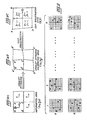
- the general problem of stitching and registration is to transform between three grids as shown in Figures 4A, 4B and 4C.
- This grid could be accessed by applying voltages V x x o , Vy Yo to an ideal hypothetical array optical system which is both perfect in construction and linear in deflection as observed in the target plane. This grid is congruentto all lenslets.
- the second grid is the lenslet stitching calibration grid which is accessed by real voltages V x (X 0 ,Y 0 ) and Vy(x o ,y o ).
- the corners of this grid are determined by the actual physical locations of fiducial marks.
- the positions of interior points within this grid relative to the corners are determined by three main factors which are: firstly, the non-linear relation between deflection voltage and spot position at a target associated with all electron optical systems; secondly, the deviations from perfection in the construction of the array optical system such as variations from lenslet to lenslet in dimensions and placement of the various elements such as array deflector bars and the lenslets in the lens array: and thirdly, the form of the equations used to map ideal voltages from the ideal mathematical grid into real voltages associated with the lenslet stitching grid.
- Lenslet stitching requires mapping of the mathematical grid a bed into the lenslet stitching grid a' b' c' d' with a sufficient number of non-linear voltage terms such that the lines connecting the corners of the mathematical grid and which define the boundaries between lenslets in mathematical space are mapped into two such boundary lines on the lenslet stitching grid (one for each lenslet), which are sufficiently close together such as to be within the acceptable range of stitching error.
- the required mapping equation between the mathematical grid and the lenslet stitching grid depends on the specifications for stitching accuracy.
- constants C and D are determined for each lenslet by measuring the voltages Vx and V y which place the beam at the positions of the lenslet stitching grid fiducial marks, and the values of x o and yo are taken as (1,1), (1,-1), (-1,-1) and (-1,1) at the fiducial marks corresponding to the appropriate mathematical grid corners.
- Constants g and h for non-linear pincushion distortion (g 01 , and h 10 ) and non-linear gain (g 10 and h o1 ) can be quite accurately determined by computer simulation of the properties of the array optical fine deflector.
- the constants V. and Vy are the nominal full-field deflection voltages, which may be found experimentally or by computer simulation.
- the positions of the fiducials marks on each lenslet stitching calibration grid may be measured using firstly a laser interferometer calibrated stage for coarse positioning over each fiducial mark and secondly an electron beam column to locate fiducial mark centres precisely. From these measurements the deviations between the position of each lenslet stitching grid fiducial mark and its location on an ideal, mathematical grid, are obtained. These deviations would then be used to modify equations (1) and (2), to provide a precisely mapped lenslet stitching calibration grid.
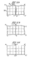
- FIG. 12A This figure depicts a 3x3 lenslet array and corresponding lenslet stitching calibration grid 70 with corners A, B, C, D. For clarity only the outer boundary of this grid is shown, along with the underlying mathematical grid 73. Now in order to write a larger area, say for example an area requiring 3x6 lenslets, it is necessary to translate the workpiece by a distance corresponding to 3 lenslets.
- the mapping of the lenslet stitching calibration grid into the workpiece in this new position is designated as A'B'C'D'.
- FIGs 12B and 12C Two methods of achieving mechanical stitching are shown in Figures 12B and 12C.
- the lenslet stitching calibration grid ABCDEF is made large enough to cover the entire area of the pattern which is to be written (3x6 lenslets).
- the boundary BE is stitched by using the methods described in connection with the chip registration grid.
- FIG. 12C A second method of achieving mechanical registration is shown in Figure 12C.
- the lenslet stitching calibration grid is only as large as the lenslet array but now the deviations from a perfect orthogonal mathematical grid are measured by some independent means, such as by using a laser controlled stage in combination with an electron beam, and the measured position of the fiducial marks used as data to insert corrections such as to make the lenslet stitching calibration grid appear to be a perfect orthogonal grid.
- the boundaries BC and A'D' can be made to match and hence mechanical stitching can be accomplished.
- Chip mapping requires that the grid ABCD shown in Figure 4C be mapped into A'B'C'D shown in Figure 4B.
- a particularly convenient way to achieve this is to first transform the chip grid described by X and Y into the mathematical grid described by x o and y o , where the variables X and Y describing the chip registration grid are of the same ideal hypothetical form as described previously for the mathematical grid variables x o and y o , but defined over a chip covered by the field of view of a multiplicity of lenslets.
- the appropriate equations are which contain only linear terms in X and Y, based upon the assumption that all wafer insertion and processing distortions can be assumed to be linear over a chip.
- the constants E and F again describe the same topological effects as the corresponding constants C and D described above, but on a chip rather than a lenslet level.
- the values of x o and y o associated with the voltages V . and Vy which are required to reach the co-responding chip registration fiducial marks from each corner lenslet are determined by use of the mapping equations (1) and (2).
- the procedure is to measure V x and Vy required to deflect the beam to the chip registration fiducial marks and then use equation (1) and (2) with the values of the C's and D's previously determined for each lenslet as described above to solve these equations for the four pairs of values for x o and y o '.
- Fiducial marks may also be supplied at a plurality of positions along chip boundaries to provide redundancy for determining with higher reliability the constants in equations (3) and (4), or their augmented versions.
- fiducial marks may be supplied within the interiors of the chips in order to be able to write continuous patterns on the same chip using two or more adjacent stage positions, for example because the chip size is larger than the array size.
- the additional fiducial marks are located at points along the boundaries between regions of the chip written at different stage positions.
- Figure 5A depicts a two-lenslet chip having chip registration marks at the corners of the chip
- Figure 5B shows the position in which the lenslet stitching grid was initially inserted when determining the stitching coefficients constants (C and D of equations (1) and (2)) and also shows the position of a wafer which has subsequently been inserted for exposure in the EBAL system and on which a chip registration grid has been incorporated.
- the stitching algorithm will interpret the deflection voltage as indicating that the target has been locally shifted to the right by the horizontal distance between A, and A' or the amount ⁇ 1 , as shown in Figure 5B.
- the stitching algorithm will indicate that the target has been locally shifted to the left by the distance ⁇ 2 , which for this example is equal to 0,.
- the chip to lenslet mapping, equations (3) and (4), will interpret these shifts as a contraction, which it will attempt to correct via the constants E, o (and F 01 ).
- the stitching error due to incorrect height placement can be corrected by utilising the well-known properties of stereoscopic vision, which can be applied to the present problem by viewing the chip fiducial marks from two adjacent lenslets.
- stereoscopic vision which can be applied to the present problem by viewing the chip fiducial marks from two adjacent lenslets.
- a more complete theory must take account of displacement and rotation effects of the chip registration grid in the x'-plane as well as tilt of the x'-plane.
- the preferred method of applying the necessary corrections to obtain stitching is to modify the constants G and H of equations (5) and (6) in an appropriate way which can be readily derived by those skilled in the art. By these means stitching can be achieved even though the workpiece (containing the chip registration grid) and the lenslet stitching grid are not inserted in the same position in the electron optical column.
- FIG. 6 illustrates two exposure stations A and B each having a fly's eye electron beam optical column wherein four chips are exposed with sixteen lenslets required to cover each chip and with flawed lenslets X which are different in stations A and B.
- the total system consists of N pairs of A and B stations for a total of 2N stations all operating in parallel.
- the first step in processing a wafer is to simultaneously expose a wafer in each station pair such as A-1 and B-1. Common coarse deflection lenslet selection is used for both stations A-1 and B-1 but the electron beams are selectively blanked when accessing a flawed lenslet.
- M the number of electron beam optical columns in the EBAL apparatus which share common spot selection, coarse deflection, and pattern-dependent fine deflection control plus pattern generating software
- M the throughput is maximum at 99% which is desirable; however, for EBAL apparatus containing a total of 36 columns, the cost of 36 independent spot selection controls, coarse deflection controls, and partial fine deflection controls, plus independent pattern generating software, will be considerable.
- the preferred configuration, for which a high lenslet yield is required e.g. 99.5% for 36 columns
- M the preferred configuration, for which a high lenslet yield is required (e.g. 99.5% for 36 columns)
- M the cost to be equal to the total number of electron beam optical columns, thereby minimising the cost of complicated and expensive deflection and pattern generating hardware and software.
- all of the cost elements of the apparatus must be known and also the cost of throughput must be determined in specific manufacturing environments before a determination of the most cost effective value for M can be made.
- Figure 8A depicts the first exposure of a wafer in quadrant 2 followed by rotation of the wafer with the rotation centre in the lower right quadrant of the electron beam optical column of the fly's eye electron beam tube whereby quadrants 1, 4 and 3 or alternatively for opposite direction of rotation quadrants 3, 4 and 1 would be successively exposed by 90° rotations of the wafer about the rotation centre in the lower right quadrant of the electron beam optical column.
- a second or permuted exposure of the target wafer us discussed above can be achieved simply by physical displacement of the rotation centre of the workpiece following the first set of exposures to a different physical location as illustrated in Figure 8B wherein the centre of rotation is physically displaced to the lower left quadrant of the optical column.
- Figure 8C of the drawing discloses the second (permuted) exposure of the same target wafer in quadrant 2 after physical displacement of the centre of the rotation to the lower left quadrant of the electron beam optical column pursuant to Figure 8B.
- Figures 8A to 8C a 7.5 cm (3 inch) electron beam optical column and a 12.7 cm (5 inch) target wafer are drawn to scale and superimposed one over the other so as to illustrate the effect of a flawed lenslet whose field of view is depicted by a dotted line small square appearing in Figure 8B in the upper left corner of quadrant 2 of the semiconductor wafer.
- the flawed lenslet itself remains fixed in space and hence will appear as shown in Figures 8B and 8C after physical displacement of the centre of rotation of the wafer.
- an extended lenslet stitching calibration grid is used.
- This grid which replaces the usual lenslet stitching calibration grid, has additional contiguous rows and columns of fiducial marks to achieve stitching after displacement of the semiconductor wafer or other target as described above.
- Figure 9A is a functional block diagram which illustrates schematically the construction of an EBAL station in a preferred configuration sharing spot selection, coarse deflection, pattern-dependent fine deflection, and pattern generating software and which employs a fly's eye electron beam column having an outer evacuated exposure station chamber 11 connected at each of the ends thereof to a suitable vacuum system for separately evacuating the end of the chamber in which an electron gun having a cathode 12 is mounted as well as the opposite end of the chamber in which the target semiconductor wafer to be processed is mounted.
- the electron gun shown generally by an electron cathode 12 is mounted at one end of station chamber 11 so as to project a finely focussed electron beam depicted by dash dot line 13 toward the opposite end of the electron beam optical column on which an object 14 such as a target workpiece, semiconductor wafer, or stitching calibration grid is supported.
- the object 14 is supported within a holder 15 which also supports a plurality of fiducial marking detectors 16 that are disposed under the fiducial marking holes formed in the object 14 for stitching and registration purposes as described previously.
- the shaft 20 is designed to be rotated by a workpiece support rotation mechanism 22 of conventional construction, the mechanism 22 and the shaft 20 being physically translatable between one or two fixed positions at either end of the travel of the bellows 21A by a workpiece stage translation mechanism 23.
- the mechanisms 22, 23 can be mounted exterior of the evacuated chamber 11 for physical rotation about the new centre of rotation, as was described above with respect to Figures 8A through 8C.
- the mechanism 22 which can comprise an electric motor of conventional construction suitably geared down to the desired rotational speeds and the mechanism 23 can comprise a linear electric motor, are under the control of a stage control 60 which in turn is under control of a system executive computer 24, which includes the pattern memory.
- the electron beam produced by the electron gun which includes the cathode 12 first passes through a set of blanking electrodes 31 which are positioned to deflect the electron beam off of an aperture onto an opaque plate for cutting of or blanking the beam from reaching the target.
- the beam passes through a beam spot selection optical system 32 for determining the size and the shape of the electron beam spot, a beam steering deflector 33 for aligning the electron beam with the axis of a coarse deflector 35 for deflecting the beam 13 to the entrance of a particular lenslet in a lenslet assembly 36 and a stigmator 34 for correcting astigmatism introduced by a fine deflector assembly 37 or for correcting for mechanical imperfections in the optical system which also can cause astigmatism.
- the lenslet assembly 36 is shown at the far end of the coarse deflector 35 and is followed by the fine deflector assembly 37.
- the coarse deflector 35 may be of the type described in U.S. Patent Specification No. 4 142 132.
- the lenslet assembly 36 and the fine deflector assembly 37 may be of the type described in U.S. Patent Specification No. 4 200 794.
- the lenslet stopping aperture 38 After passing through the fine deflector assembly 37, the electron beam 13 then must pass through a lenslet stopping aperture 38 which is mechanically coupled through a connection 39 to a lenslet stopping aperture control 41.
- the construction of the lenslet stopping aperture is best seen in Figures 10A and 10B of the drawings.
- the lenslet stopping aperture comprises two rolls 38A, 38B of an electron stopping material rolled on calender rolls that can be rolled either up or down or right and left as shown in Figure 10A.
- the rolls 38A, 38B of electron beam stopping material each have a respective elongated slit 42, 43 formed therein and extending width-wise across the material.
- the slits 42, 43 are so positioned as to intersect one another within their range of movement.
- the tolerances on the size and shape of this opening might typically be of the order of 10% or more of the dimensions of the lenslet field itself.
- the rolls 38A, 38B are activated. If, for example, the slit 43 is moved to the right, the opening will move to the right from the position shown in Figure 10A and if it is moved left by appropriately rolling up one of the rolls and paying out on the other, the opening will move to the left. Similarly, if the upper roll is taken up and the lower roll is payed out to control the positioning of the electron stopping material in which the slit 42 is formed, the opening will move up from the position shown in Figure 10A and if the rolls are moved in the reverse direction, the opening can be caused to move downwardly.
- the lenslet stopping aperture which is formed by the alignment of the two slits 42, 43 at their intersection, can be caused to move in an X, Y plane over the entire surface of the object 14.
- the lenslet stopping aperture control 41 controls payout and takeup of the rolls 38A, 38B which control positioning of the opening defined by the slits 42, 43 via the interconnection 39.
- An EBAL station constructed as shown in Figure 9A should employ a cathode which combines adequate brightness and low operating temperature with long life in a demountable vacuum chamber which is occasionally exposed to ambient air. Furthermore, the cathode should be designed for periodic replacement in demountable hardware.
- a possible cathode would be tungsten having a brightness of approximately 3x 10⁴ amperes per square centimetre per sterradian and an even better choice having higher brightness would be a lanthanum hexaboride which can operate at a brightness of about 4x10 5 amperes per square centimetre per sterradian.
- Power for the cathode and electron gun is from high voltage and cathode power supply 51 under the control of the system executive computer 24.
- the electrodes 31 are of conventional known construction and are under the control of an electron beam blanker control 52 which is in turn controlled by the individual station computer 19.
- the beam spot size and shape selection optical system 32 is of conventional known construction as described, for example, in the paper entitled “Electron Beam Direct Writing Lithography System” by J. Trotel, published in The Proceedings of the International Conference on Microlithography, Amsterdam, 30 Sept.-2 Oct. 1980, p. 111 (Delft University Press, 1981) and is under the control of an electron beam spot selectron control circuit 53 that, in turn, is controlled by the system executive computer 24.
- the beam steering deflector 33 which corrects for misalignment betweent he electron gun and the coarse deflector 35, is of conventional, known construction and is under the control of an electron beam steering control circuit 54 of conventional design and is in turn controlled by the individual station computer 19.
- the basic principles of the stigmator 34 and its associated stigmation control 55 are known and are under the control of both the system executive computer 24 and the individual station computer 19.
- the coarse deflector 35 and its associated coarse deflection controLcircuit 56, together with correction capability, are described more fully in U.S. Patent Specification No. 4 142 132 and are in turn controlled by the system executive computer 24.
- the lenslet assembly 36 is supplied with a constant focusing voltage from a power supply 51 and a variable dynamic focusing voltage, as described more fully is published European Patent Application No. 0 033 805, from an array lens dynamic focus control 57, which in turn is controlled by both the system executive computer 24 and the individual station computer 19.
- the fine deflector assembly 37 is controlled by a pattern-dependent fine deflection control 58, which in turn is controlled by the system executive computer 24, and corrected by a fine deflector correction 59 which, in turn, is controlled by the individual station computer 19.
- the system executive computer 24 may be common to all the EBAL stations comprising the EBAL apparatus, each station of which is similar to that shown in Figure 9A.
- the power supply 51, the coarse deflection control 56, the pattern dependent fine deflection control 58, and the lenslet stopping aperture control 41 may be common to some or all of the EBAL stations under the control of the system executive computer 24.
- Figure 11 shows such a system, consisting of a number of EBAL stations such as shown in Figure 9A.
- the EBAL apparatus contains N stations which are divided into m subgroups of M stations each, and that these subgroups share a set of electronic control circuits 63 which include spot selection control 53, coarse deflection control 56, lenslet stopping aperture control 41, pattern dependent fine deflection control 58, a flawed lenslet pattern memory 62, and a subgroup computer 64 in which some of the functions reside that were carried out by the system executive computer 24 in the apparatus composed of stations shown in Figure 9A.
- each station is provided with an individual control circuit 66 in the form of the blanker control 52, the beam steering control 54, the stigmation control 55, the array lens dynamic focus control 57, the fine deflection correction control 59, the fiducial signal processor 18, and the individual station computer 19 within which are found circuits for stitching and registration and flawed lenslet mapping.
- a set of electronics 61 is associated with all N stations which include the power supply 51, the stage control 60, a complete pattern memory 65, and the system executive computer 24.
- the flawed lenslet mapping memory is used to selectively blank the electron beam in those stations which have a flawed lenslet at the particular lenslet location which is currently being exposed.
- the flawed lenslet mapping memory is used to control the exposure of only flawed lenslets.
- the above described EBAL apparatus is particularly designed for use un the fabrication of semiconductor integrated circuits of the LSI and VLSI type either in the form of reticles, masks of directly written patterns on wafers.
- the EBAL apparatus employs an electron beam electron optical column of the fly's eye type wherein an array lenslet assembly is employed in conjunction with an associated array deflector assembly to provide precise and extremely fine detailed control over the positioning of the electron beam with respect to the surface of a workpiece during exposure with the electron beam.
- the EBAL apparatus is designed such that while the field of view of each lenslet in the array optical system employed in the fly's eye electron beam column is not large enough to cover a complete circuit pattern, the fields of view of a number of adjacent lenslets can be stitched together at the workpiece surface so as to cover the entire surface. Electron beam registration between adjacent lenslets and between successive superimposed levels of materials deposited or otherwise formed on the surface of the target workpieces is achieved through the use of a registration scheme employing fiducial marking signals derived from the surface of the target wafer. The effect of any flawed lenslets in the array are overcome through the use of a permutation scheme in which areas on the target workpiece surface that otherwise would be affected by a flawed lenslet are rewritten so as greatly to increase the yield of IC circuits produced.
Landscapes
- Engineering & Computer Science (AREA)
- Chemical & Material Sciences (AREA)
- Nanotechnology (AREA)
- Crystallography & Structural Chemistry (AREA)
- Physics & Mathematics (AREA)
- Analytical Chemistry (AREA)
- Mathematical Physics (AREA)
- Theoretical Computer Science (AREA)
- Condensed Matter Physics & Semiconductors (AREA)
- General Physics & Mathematics (AREA)
- Manufacturing & Machinery (AREA)
- Electron Beam Exposure (AREA)
- Exposure And Positioning Against Photoresist Photosensitive Materials (AREA)
Claims (31)




Applications Claiming Priority (2)
| Application Number | Priority Date | Filing Date | Title |
|---|---|---|---|
| US06/254,870 US4430571A (en) | 1981-04-16 | 1981-04-16 | Method and apparatus for exposing multi-level registered patterns interchangeably between stations of a multi-station electron-beam array lithography (EBAL) system |
| US254870 | 1981-04-16 |
Publications (3)
| Publication Number | Publication Date |
|---|---|
| EP0063429A2 EP0063429A2 (fr) | 1982-10-27 |
| EP0063429A3 EP0063429A3 (en) | 1984-01-04 |
| EP0063429B1 true EP0063429B1 (fr) | 1986-10-08 |
Family
ID=22965911
Family Applications (1)
| Application Number | Title | Priority Date | Filing Date |
|---|---|---|---|
| EP82301670A Expired EP0063429B1 (fr) | 1981-04-16 | 1982-03-30 | Appareil de lithographie par matrice de faisceaux d'électrons et méthode pour son utilisation |
Country Status (6)
| Country | Link |
|---|---|
| US (1) | US4430571A (fr) |
| EP (1) | EP0063429B1 (fr) |
| JP (1) | JPS57181122A (fr) |
| AU (2) | AU549326B2 (fr) |
| CA (1) | CA1166362A (fr) |
| DE (1) | DE3273692D1 (fr) |
Families Citing this family (36)
| Publication number | Priority date | Publication date | Assignee | Title |
|---|---|---|---|---|
| JPS57208132A (en) * | 1981-06-17 | 1982-12-21 | Toshiba Corp | Electron-beam exposure apparatus |
| JPS59124719A (ja) * | 1982-12-29 | 1984-07-18 | Fujitsu Ltd | 電子ビ−ム露光装置 |
| US4613981A (en) * | 1984-01-24 | 1986-09-23 | Varian Associates, Inc. | Method and apparatus for lithographic rotate and repeat processing |
| DE3410885A1 (de) * | 1984-03-24 | 1985-10-03 | Ibm Deutschland Gmbh, 7000 Stuttgart | Fehlerkorrigierte korpuskularstrahllithographie |
| JPS6246518A (ja) * | 1985-08-23 | 1987-02-28 | Toshiba Corp | 荷電ビ−ム描画方法 |
| JPS6298724A (ja) * | 1985-10-25 | 1987-05-08 | Hitachi Ltd | 電子線描画装置 |
| US4890239A (en) * | 1987-10-20 | 1989-12-26 | Shipley Company, Inc. | Lithographic process analysis and control system |
| US5012105A (en) * | 1989-02-02 | 1991-04-30 | Nippon Seiko Kabushiki Kaisha | Multiple-imaging charged particle-beam exposure system |
| US5280437A (en) * | 1991-06-28 | 1994-01-18 | Digital Equipment Corporation | Structure and method for direct calibration of registration measurement systems to actual semiconductor wafer process topography |
| JPH05206017A (ja) * | 1991-08-09 | 1993-08-13 | Internatl Business Mach Corp <Ibm> | リソグラフイ露光システム及びその方法 |
| JP3796317B2 (ja) * | 1996-06-12 | 2006-07-12 | キヤノン株式会社 | 電子ビーム露光方法及びそれを用いたデバイス製造方法 |
| US5798528A (en) * | 1997-03-11 | 1998-08-25 | International Business Machines Corporation | Correction of pattern dependent position errors in electron beam lithography |
| SE9800665D0 (sv) * | 1998-03-02 | 1998-03-02 | Micronic Laser Systems Ab | Improved method for projection printing using a micromirror SLM |
| JPH11329928A (ja) * | 1998-05-12 | 1999-11-30 | Advantest Corp | 電子ビーム露光装置 |
| IL125338A0 (en) * | 1998-07-14 | 1999-03-12 | Nova Measuring Instr Ltd | Method and apparatus for monitoring and control of photolithography exposure and processing tools |
| JP3982913B2 (ja) * | 1998-07-17 | 2007-09-26 | 株式会社アドバンテスト | 荷電粒子ビーム露光装置 |
| US6556702B1 (en) * | 1999-01-06 | 2003-04-29 | Applied Materials, Inc. | Method and apparatus that determines charged particle beam shape codes |
| WO2001039243A1 (fr) * | 1999-11-23 | 2001-05-31 | Ion Diagnostics, Inc. | Optique electronique destinee a un outil lithographique faisceau electronique multi-faisceaux |
| WO2001060456A1 (fr) | 2000-02-19 | 2001-08-23 | Ion Diagnostics, Inc. | Systeme d'inspection a faisceaux d'electrons a plusieurs colonnes et faisceaux |
| US6943351B2 (en) * | 2000-02-19 | 2005-09-13 | Multibeam Systems, Inc. | Multi-column charged particle optics assembly |
| US6734428B2 (en) | 2000-02-19 | 2004-05-11 | Multibeam Systems, Inc. | Multi-beam multi-column electron beam inspection system |
| US7122795B2 (en) * | 2001-04-18 | 2006-10-17 | Multibeam Systems, Inc. | Detector optics for charged particle beam inspection system |
| KR100523823B1 (ko) * | 2002-06-13 | 2005-10-25 | 에이에스엠엘 네델란즈 비.브이. | 리소그래피장치 및 디바이스제조방법 |
| US6785615B2 (en) * | 2002-10-29 | 2004-08-31 | International Business Machines Corporation | Method and structure for detection of electromechanical problems using variance statistics in an E-beam lithography device |
| US8064730B2 (en) * | 2003-09-22 | 2011-11-22 | Asml Netherlands B.V. | Device manufacturing method, orientation determination method and lithographic apparatus |
| JP4313145B2 (ja) * | 2003-10-07 | 2009-08-12 | 株式会社日立ハイテクノロジーズ | 荷電粒子ビーム描画方法及び荷電粒子ビーム描画装置 |
| JP4611755B2 (ja) * | 2005-01-13 | 2011-01-12 | 株式会社日立ハイテクノロジーズ | 走査電子顕微鏡及びその撮像方法 |
| CN101248505B (zh) * | 2005-07-08 | 2010-12-15 | 耐克斯金思美控股公司 | 受控粒子束制造用的设备和方法 |
| WO2008140585A1 (fr) | 2006-11-22 | 2008-11-20 | Nexgen Semi Holding, Inc. | Appareil et procédé de fabrication de masque conforme |
| US10991545B2 (en) | 2008-06-30 | 2021-04-27 | Nexgen Semi Holding, Inc. | Method and device for spatial charged particle bunching |
| US10566169B1 (en) | 2008-06-30 | 2020-02-18 | Nexgen Semi Holding, Inc. | Method and device for spatial charged particle bunching |
| CN102460631B (zh) * | 2009-05-20 | 2015-03-25 | 迈普尔平版印刷Ip有限公司 | 两次扫描 |
| JP5386544B2 (ja) * | 2011-06-07 | 2014-01-15 | 株式会社アドバンテスト | 電子ビーム露光装置及び電子ビーム露光方法 |
| US10593074B1 (en) * | 2016-03-16 | 2020-03-17 | Liberty Mutual Insurance Company | Interactive user interface for displaying geographic boundaries |
| US12493005B1 (en) | 2022-06-07 | 2025-12-09 | Nexgen Semi Holding, Inc. | Extended range active illumination imager |
| CN119943633B (zh) * | 2025-04-07 | 2025-06-17 | 惠然科技有限公司 | 带电粒子束系统中视场缝合的方法、电子设备和存储介质 |
Family Cites Families (3)
| Publication number | Priority date | Publication date | Assignee | Title |
|---|---|---|---|---|
| US3789185A (en) | 1969-12-15 | 1974-01-29 | Ibm | Electron beam deflection control apparatus |
| JPS52109373A (en) * | 1976-03-10 | 1977-09-13 | Rikagaku Kenkyusho | Method of deflecting and scanning electron beam |
| US4200794A (en) * | 1978-11-08 | 1980-04-29 | Control Data Corporation | Micro lens array and micro deflector assembly for fly's eye electron beam tubes using silicon components and techniques of fabrication and assembly |
-
1981
- 1981-04-16 US US06/254,870 patent/US4430571A/en not_active Expired - Lifetime
-
1982
- 1982-03-30 DE DE8282301670T patent/DE3273692D1/de not_active Expired
- 1982-03-30 EP EP82301670A patent/EP0063429B1/fr not_active Expired
- 1982-03-31 CA CA000399901A patent/CA1166362A/fr not_active Expired
- 1982-04-07 AU AU82425/82A patent/AU549326B2/en not_active Ceased
- 1982-04-15 JP JP57063209A patent/JPS57181122A/ja active Pending
-
1985
- 1985-11-13 AU AU49864/85A patent/AU577640B2/en not_active Ceased
Also Published As
| Publication number | Publication date |
|---|---|
| AU4986485A (en) | 1986-03-20 |
| EP0063429A2 (fr) | 1982-10-27 |
| AU8242582A (en) | 1982-10-21 |
| DE3273692D1 (en) | 1986-11-13 |
| CA1166362A (fr) | 1984-04-24 |
| AU549326B2 (en) | 1986-01-23 |
| JPS57181122A (en) | 1982-11-08 |
| AU577640B2 (en) | 1988-09-29 |
| EP0063429A3 (en) | 1984-01-04 |
| US4430571A (en) | 1984-02-07 |
Similar Documents
| Publication | Publication Date | Title |
|---|---|---|
| EP0063429B1 (fr) | Appareil de lithographie par matrice de faisceaux d'électrons et méthode pour son utilisation | |
| US4467211A (en) | Method and apparatus for exposing multi-level registered patterns interchangeably between stations of a multi-station electron-beam array lithography (EBAL) system | |
| US4390789A (en) | Electron beam array lithography system employing multiple parallel array optics channels and method of operation | |
| US5401972A (en) | Layout overlay for FIB operations | |
| EP0660370B1 (fr) | Système de lithographie par faisceau d'électrons | |
| US4213053A (en) | Electron beam system with character projection capability | |
| US4694178A (en) | Multiple channel electron beam optical column lithography system and method of operation | |
| US5757409A (en) | Exposure method and pattern data preparation system therefor, pattern data preparation method and mask as well as exposure apparatus | |
| US4442361A (en) | System and method for calibrating electron beam systems | |
| US6835511B2 (en) | Methods and apparatus for detecting and correcting reticle deformations in microlithography | |
| US9087366B2 (en) | High accuracy beam placement for local area navigation | |
| JPH1064799A (ja) | 荷電ビーム描画装置及び描画方法 | |
| JP2020053380A (ja) | マルチ電子ビーム画像取得装置及びマルチ電子ビーム画像取得方法 | |
| US6277532B1 (en) | Charged-particle-beam microlithographic methods for correction of reticle distortions | |
| US5674413A (en) | Scattering reticle for electron beam systems | |
| JP2019114731A (ja) | マルチ荷電粒子ビーム描画装置及びマルチ荷電粒子ビーム描画方法 | |
| CN111812947A (zh) | 多带电粒子束描绘装置以及多带电粒子束描绘方法 | |
| EP0033138B1 (fr) | Procédé pour corriger les distorsions de déviation dans un appareil pour lithographie à particules chargées | |
| GB2109538A (en) | Electron beam alignment | |
| US6291819B1 (en) | Method of calibrating an electron beam system for lithography | |
| JPH10106931A (ja) | 電子ビーム露光方法およびそれを用いた半導体集積回路装置の製造方法 | |
| US4835392A (en) | Ion-projection apparatus | |
| US4424450A (en) | Hybrid moving stage and rastered electron beam lithography system employing approximate correction circuit | |
| JP2001015428A (ja) | 電子ビーム露光装置 | |
| JP3105657B2 (ja) | 荷電粒子ビーム描画方法 |
Legal Events
| Date | Code | Title | Description |
|---|---|---|---|
| PUAI | Public reference made under article 153(3) epc to a published international application that has entered the european phase |
Free format text: ORIGINAL CODE: 0009012 |
|
| AK | Designated contracting states |
Designated state(s): DE FR GB |
|
| PUAL | Search report despatched |
Free format text: ORIGINAL CODE: 0009013 |
|
| AK | Designated contracting states |
Designated state(s): DE FR GB |
|
| 17P | Request for examination filed |
Effective date: 19840604 |
|
| GRAA | (expected) grant |
Free format text: ORIGINAL CODE: 0009210 |
|
| AK | Designated contracting states |
Kind code of ref document: B1 Designated state(s): DE FR GB |
|
| ET | Fr: translation filed | ||
| REF | Corresponds to: |
Ref document number: 3273692 Country of ref document: DE Date of ref document: 19861113 |
|
| PLBE | No opposition filed within time limit |
Free format text: ORIGINAL CODE: 0009261 |
|
| STAA | Information on the status of an ep patent application or granted ep patent |
Free format text: STATUS: NO OPPOSITION FILED WITHIN TIME LIMIT |
|
| 26N | No opposition filed | ||
| PGFP | Annual fee paid to national office [announced via postgrant information from national office to epo] |
Ref country code: FR Payment date: 19910224 Year of fee payment: 10 |
|
| PGFP | Annual fee paid to national office [announced via postgrant information from national office to epo] |
Ref country code: DE Payment date: 19910227 Year of fee payment: 10 |
|
| PGFP | Annual fee paid to national office [announced via postgrant information from national office to epo] |
Ref country code: GB Payment date: 19910301 Year of fee payment: 10 |
|
| PG25 | Lapsed in a contracting state [announced via postgrant information from national office to epo] |
Ref country code: GB Effective date: 19920330 |
|
| GBPC | Gb: european patent ceased through non-payment of renewal fee | ||
| PG25 | Lapsed in a contracting state [announced via postgrant information from national office to epo] |
Ref country code: FR Effective date: 19921130 |
|
| PG25 | Lapsed in a contracting state [announced via postgrant information from national office to epo] |
Ref country code: DE Effective date: 19921201 |
|
| REG | Reference to a national code |
Ref country code: FR Ref legal event code: ST |