EP0063851B1 - Clavier à interrupteurs transparent - Google Patents
Clavier à interrupteurs transparent Download PDFInfo
- Publication number
- EP0063851B1 EP0063851B1 EP82300075A EP82300075A EP0063851B1 EP 0063851 B1 EP0063851 B1 EP 0063851B1 EP 82300075 A EP82300075 A EP 82300075A EP 82300075 A EP82300075 A EP 82300075A EP 0063851 B1 EP0063851 B1 EP 0063851B1
- Authority
- EP
- European Patent Office
- Prior art keywords
- backplate
- flexible sheet
- conductive strips
- switch array
- conductive
- Prior art date
- Legal status (The legal status is an assumption and is not a legal conclusion. Google has not performed a legal analysis and makes no representation as to the accuracy of the status listed.)
- Expired
Links
- 239000000463 material Substances 0.000 claims description 37
- 239000010410 layer Substances 0.000 claims description 18
- 239000004020 conductor Substances 0.000 claims description 17
- GWEVSGVZZGPLCZ-UHFFFAOYSA-N Titan oxide Chemical compound O=[Ti]=O GWEVSGVZZGPLCZ-UHFFFAOYSA-N 0.000 claims description 12
- PCHJSUWPFVWCPO-UHFFFAOYSA-N gold Chemical compound [Au] PCHJSUWPFVWCPO-UHFFFAOYSA-N 0.000 claims description 9
- 239000010931 gold Substances 0.000 claims description 9
- 238000000034 method Methods 0.000 claims description 9
- 229910052737 gold Inorganic materials 0.000 claims description 8
- MRNHPUHPBOKKQT-UHFFFAOYSA-N indium;tin;hydrate Chemical compound O.[In].[Sn] MRNHPUHPBOKKQT-UHFFFAOYSA-N 0.000 claims description 8
- 239000010409 thin film Substances 0.000 claims description 8
- 230000005855 radiation Effects 0.000 claims description 7
- 238000000926 separation method Methods 0.000 claims description 7
- 239000002344 surface layer Substances 0.000 claims description 6
- 239000004408 titanium dioxide Substances 0.000 claims description 6
- 239000011159 matrix material Substances 0.000 claims description 5
- 229910052751 metal Inorganic materials 0.000 claims description 5
- 239000002184 metal Substances 0.000 claims description 5
- 230000002093 peripheral effect Effects 0.000 claims description 3
- 229920002379 silicone rubber Polymers 0.000 claims description 3
- 230000008569 process Effects 0.000 claims description 2
- 238000013035 low temperature curing Methods 0.000 claims 1
- 238000000576 coating method Methods 0.000 description 26
- 239000011248 coating agent Substances 0.000 description 16
- 230000003287 optical effect Effects 0.000 description 11
- 239000000853 adhesive Substances 0.000 description 10
- 230000001070 adhesive effect Effects 0.000 description 10
- 239000010408 film Substances 0.000 description 8
- 238000003491 array Methods 0.000 description 7
- 239000000758 substrate Substances 0.000 description 7
- KDLHZDBZIXYQEI-UHFFFAOYSA-N Palladium Chemical compound [Pd] KDLHZDBZIXYQEI-UHFFFAOYSA-N 0.000 description 6
- BASFCYQUMIYNBI-UHFFFAOYSA-N platinum Chemical compound [Pt] BASFCYQUMIYNBI-UHFFFAOYSA-N 0.000 description 6
- 238000005424 photoluminescence Methods 0.000 description 5
- 229920006267 polyester film Polymers 0.000 description 5
- 238000004544 sputter deposition Methods 0.000 description 5
- CTQNGGLPUBDAKN-UHFFFAOYSA-N O-Xylene Chemical compound CC1=CC=CC=C1C CTQNGGLPUBDAKN-UHFFFAOYSA-N 0.000 description 4
- 230000000694 effects Effects 0.000 description 4
- 238000001914 filtration Methods 0.000 description 4
- 239000008096 xylene Substances 0.000 description 4
- BQCADISMDOOEFD-UHFFFAOYSA-N Silver Chemical compound [Ag] BQCADISMDOOEFD-UHFFFAOYSA-N 0.000 description 3
- 239000011324 bead Substances 0.000 description 3
- 229920001971 elastomer Polymers 0.000 description 3
- 239000000806 elastomer Substances 0.000 description 3
- 229910052763 palladium Inorganic materials 0.000 description 3
- 229910052697 platinum Inorganic materials 0.000 description 3
- 229910052709 silver Inorganic materials 0.000 description 3
- 239000004332 silver Substances 0.000 description 3
- 239000012780 transparent material Substances 0.000 description 3
- 239000004642 Polyimide Substances 0.000 description 2
- 230000008859 change Effects 0.000 description 2
- 238000000151 deposition Methods 0.000 description 2
- 239000012769 display material Substances 0.000 description 2
- 230000003993 interaction Effects 0.000 description 2
- 239000004973 liquid crystal related substance Substances 0.000 description 2
- 238000004519 manufacturing process Methods 0.000 description 2
- 238000007747 plating Methods 0.000 description 2
- 229920001721 polyimide Polymers 0.000 description 2
- 229920000642 polymer Polymers 0.000 description 2
- 238000003825 pressing Methods 0.000 description 2
- 230000008439 repair process Effects 0.000 description 2
- 229910052710 silicon Inorganic materials 0.000 description 2
- 239000010703 silicon Substances 0.000 description 2
- 238000001228 spectrum Methods 0.000 description 2
- 238000007736 thin film deposition technique Methods 0.000 description 2
- 229910001258 titanium gold Inorganic materials 0.000 description 2
- 229920002799 BoPET Polymers 0.000 description 1
- 239000005041 Mylar™ Substances 0.000 description 1
- 229920005372 Plexiglas® Polymers 0.000 description 1
- XUIMIQQOPSSXEZ-UHFFFAOYSA-N Silicon Chemical compound [Si] XUIMIQQOPSSXEZ-UHFFFAOYSA-N 0.000 description 1
- 238000005275 alloying Methods 0.000 description 1
- 230000004075 alteration Effects 0.000 description 1
- 230000015556 catabolic process Effects 0.000 description 1
- 238000007796 conventional method Methods 0.000 description 1
- 238000006731 degradation reaction Methods 0.000 description 1
- 238000010894 electron beam technology Methods 0.000 description 1
- 230000007613 environmental effect Effects 0.000 description 1
- 238000005530 etching Methods 0.000 description 1
- 238000001704 evaporation Methods 0.000 description 1
- 230000008020 evaporation Effects 0.000 description 1
- 230000005284 excitation Effects 0.000 description 1
- 230000001747 exhibiting effect Effects 0.000 description 1
- 238000002474 experimental method Methods 0.000 description 1
- 238000009501 film coating Methods 0.000 description 1
- ZNKMCMOJCDFGFT-UHFFFAOYSA-N gold titanium Chemical compound [Ti].[Au] ZNKMCMOJCDFGFT-UHFFFAOYSA-N 0.000 description 1
- 238000004020 luminiscence type Methods 0.000 description 1
- 238000003754 machining Methods 0.000 description 1
- 238000012986 modification Methods 0.000 description 1
- 230000004048 modification Effects 0.000 description 1
- 238000000465 moulding Methods 0.000 description 1
- 239000002245 particle Substances 0.000 description 1
- -1 phosphor compound Chemical class 0.000 description 1
- 239000004033 plastic Substances 0.000 description 1
- 229920003023 plastic Polymers 0.000 description 1
- 229920000728 polyester Polymers 0.000 description 1
- 239000004926 polymethyl methacrylate Substances 0.000 description 1
- 238000012545 processing Methods 0.000 description 1
- 238000002310 reflectometry Methods 0.000 description 1
- 238000012216 screening Methods 0.000 description 1
- 239000002210 silicon-based material Substances 0.000 description 1
- 239000006104 solid solution Substances 0.000 description 1
- 239000002904 solvent Substances 0.000 description 1
- 125000006850 spacer group Chemical group 0.000 description 1
- 238000012360 testing method Methods 0.000 description 1
- 229920001169 thermoplastic Polymers 0.000 description 1
- 239000012815 thermoplastic material Substances 0.000 description 1
- 239000004416 thermosoftening plastic Substances 0.000 description 1
- 238000012549 training Methods 0.000 description 1
- 230000000007 visual effect Effects 0.000 description 1
Images

Classifications
-
- H—ELECTRICITY
- H01—ELECTRIC ELEMENTS
- H01H—ELECTRIC SWITCHES; RELAYS; SELECTORS; EMERGENCY PROTECTIVE DEVICES
- H01H13/00—Switches having rectilinearly-movable operating part or parts adapted for pushing or pulling in one direction only, e.g. push-button switch
- H01H13/70—Switches having rectilinearly-movable operating part or parts adapted for pushing or pulling in one direction only, e.g. push-button switch having a plurality of operating members associated with different sets of contacts, e.g. keyboard
- H01H13/83—Switches having rectilinearly-movable operating part or parts adapted for pushing or pulling in one direction only, e.g. push-button switch having a plurality of operating members associated with different sets of contacts, e.g. keyboard characterised by legends, e.g. Braille, liquid crystal displays, light emitting or optical elements
Definitions
- This invention relates to touch-operated switching devices. More specifically, this invention relates to rectangular arrays of pressure sensitive switching elements that are relatively transparent and thus permit various alphanumeric characters or other symbols to be viewed through the switching array.
- the type of switching array addressed by the present invention includes a relatively pliant or flexible planar sheet of material that is spaced apart from and parallel to a relatively rigid planar backplate of sustantially identical curvature.
- the surface of the backplate that faces the pliant sheet material includes n parallel strips of conductive material and the juxtaposed surface of the pliant sheet includes m conductive strips that are parallel to one another and perpendicular to the conductive strips of the backplate.
- switching devices of this type are sometimes referred to as X-Y switching arrays or X-Y selectors.
- X-Y selectors and other arrays of touch-operated switches often serve as a keyboard for use with a wide variety of electrical and electronic systems wherein human control of interaction is necessary. fn this regard, there are a growing number of situations in which it is either desired or necessary to change the function or operation defined by one or more keys within such a switching array during a particular sequence of keyboard operations or to change functions of the keys so that a completely different operational sequence can be implemented.
- a keyboard can be used advantageously in a programmed electronic instrument or system wherein operator interaction is required to sequence the system or instrument through a series of various computational steps or other operations that may vary, depending on the keys selected by the operator and/or the results of the previous step of the sequence.
- the number of switching elements required during each step of an operational sequence often varies and it may be desirable to utilize a different keyboard pattern or configuration at different steps of the sequence.
- One prior art proposal for permitting various instructions and comments to be displayed within an associated set of keys or switches that are defined in accordance with the operational step or sequence being performed utilizes an X-Yselec- tor of the above-described type that is mounted to the face of a cathode-ray tube (CRT) or a similar display device with the pliant sheet, the backplate and the conductive strips all being formed of a transparent material. Since numerous techniques are known for generating virtually any desired symbol or character with either raster scan systems (such as conventional televison) or X-Y deflectable electron gun systems (such as conventional oscilloscopes) and since most systems or instruments that include computational or programming capability can store the information required to generate a relatively large number of various displays, such an arrangement offers considerable advantages.
- prior art devices have not always allowed the characters generated on the cathode-ray tube to be observed as readily as is desired.
- the switching array must not diffuse or distort the characters produced on the cathode-ray tube.
- the display generated by the cathode-ray tube to define different switching formats that use a selected number of the arrayed .switches at selected positions within the rectangular matrix that forms the switch array, the separation between the rows and columns (and hence between the switching elements) should be as visibly indiscernible as possible.
- materials of sufficient transparency are available, the visual or optical properties of prior art devices have not been completely satisfactory.
- This document discloses the use of means, such as a thin transparent insulating grid, to prevent shorting between the conductive strips on the backplate and those on the flexible transparent sheet in places where no external pressure is present.
- This grid must cover the whole surface of the conductive strips on the surface of the backplate. Its fabrication involves several steps.
- a preferred embodiment of the new transparent switch array exhibits improved viewing of luminescent displays under various ambient lighting conditions relative to the quality of such displays in the absence of the switch array.
- one surface of the relatively transparent, rigid backplate is formed of poly-(methyl methacrylate)-type polymer or other suitable material and is coated with a thin, transparent conductive material such as a gold-titanium thin film.
- the conductive film is partitioned into a series of conductive row elements by scribing or otherwise removing a narrow region of material so as to electrically isolate each row element from the adjacent row elements. For example, a grid of parallel, spaced apart conductors of relatively small diameter is placed against the coated surface of the backplate and an electrical current is applied to, in effect, burn away narrow regions of the thin film coating and form the desired row elements.
- Conductive column elements that form the second element of each switch of the switch array are formed in a similar manner on one surface of a sheet of polyester or other transparent material that exhibits a pliancy or yielding characteristic that permits at least limited deformation or flexure when a localized pressure such as the force exerted by pressing lightly with a finger is asserted against the surface of the material.
- This pliant sheet material is positioned parallel to and spaced apart from the coated surface of the backplate with the conductive column elements facing the backplate and being substantially perpendicular to the row elements on the surface of the backplate.
- each embodiment of this invention are relatively close together, being spaced apart by a distance of less than 0.010 inch (254 microns) and preferably being spaced apart by a distance of approximately 0.8 to 1.2 mils (20 to 30 microns).
- the surface of the pliant sheet includes a geometric pattern of transparent bead-like "dots" with each dot projecting outwardly from the conductive surface of the material. More specifically, in the presently-preferred embodiments of the invention, small dots of a transparent, silicon-based elastomer are deposited on the surface of the pliant material by means of a conventional silk-screen process with the dots forming a rectangular pattern that corresponds to the pattern formed by the narrow gaps that separate adjoining conductive elements of the backplate from one another and the narrow gaps that separate column elements of the pliant sheet from one another.
- the material for forming the separation dots is selected to obtain a diffraction coefficient that is approximately equal to the square root of the diffraction coefficient of the pliant sheet member.
- a minimum numu b t jf separation dots is employed, with the presently-preferred embodiments of the invention utilizing four such dots symmetrically positioned about each intersection of the juxtaposed narrow gaps that defines the corners of four contiguous switching elements.
- the rectangular outline of each touch sensitive switch region of the array includes eight separation dots with two dots being associated with any one edge.
- each conductive row and column element Electrical contact is provided to each conductive row and column element by means of small spaced apart conductors that are formed on one surface of a thin, flexible strip of a substrate material such as a polyester film or polyimide sheet material.
- the terminal portion of each conductor of this electrical cable arrangement includes a rectangular contact region positioned so that each contact region of the cable will contact the terminal portion of an associated conductive row element when the cable is placed on the conductive surface of the backplate and routed along an edge that is perpendicular to the conductive row elements.
- the cable is folded on itself at one corner of the backplate so that the cable extends along one of the backplate edges that is parallel to the conductive row elements. This causes the conductive regions of the cable to face upwardly for contacting the terminal portions of the conductive column elements that are contained on one surface of the pliant sheet member.
- the electrical cable is maintained in the above-described position by a strip of thin, transparent material having an adhesive material deposited on each planar surface thereof.
- a strip of this double-sided adhesive material is then applied to the border region of the two remaining edges of the backplate and the pliant sheet is positioned atop the border formed by the electrical cable and the adhesive strips.
- the sandwich-like assemblage is then joined together by U - shaped spring clips that are installed along the edges of the assembly, with a clip being positoned over each contact region of the electrical cable and the juxtaposed terminal region of the associated row or column element.
- the conductive film that forms the row elements of the backplate and the column elements of the pliant sheet member is selected and arranged for substantially improved view of luminescent displays that are generated at the rear surface of the backplate by conventional cathode-ray systems, or other devices such as liquid-crystal displays and plasma-discharge display panels.
- luminescent displays that are generated at the rear surface of the backplate by conventional cathode-ray systems, or other devices such as liquid-crystal displays and plasma-discharge display panels.
- most display materials exhibit a relatively high degree of photoluminescence as well as being energizable by a primary excitation means and viewing the display under conditions of relatively high ambient light can become a problem.
- the disclosed embodiment of the invention is configured for use with a cathode-ray tube wherein the phosphor compound that coats the inside surface of the tube face is excited by an emitted electron beam (cathode luminescence) and light energy that impinges on the gloss face of the tube further excites the phosphorescent coating (photoluminescence).
- cathode luminescence emitted electron beam
- photoluminescence phosphorescent coating
- the photoluminescence can seriously hamper observance of the intended display, especially in situations wherein the display primarily depends on phosphorescence of the display material, rather than the fluorescence thereof utilizes a "high persistance" phosphorescent coating).
- the conductive coating of the switch array is selected to exhibit high transmissibility (transparency) relative to the light energy emitted by the luminescent display and high opacity (law transparency) relative to light energy that causes the photoluminescence.
- the coating or film of the preferred embodiments of the invention are, in effect, optical filters which improve the display quality while simultaneously providing the necessary electrical conductivity and durability.
- conductive films that employ an initial layer of titanium dioxide that is approximately 75 to 150 angstroms in thickness; a second layer of sputter gold that is approximately 40 to 120 angstroms thick; and a surface layer of tin-indium oxide that is approximately 150-500 angstroms in thickness provide the desired electrical conductivity and optical filtering for a cathode-ray phosphorescent material that emits light at a primary wavelength of approximately 520 nanometers.
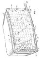
- the switch array 10 includes a planar, transparent backplate 12 having a transparent conductive coating 14 that forms a number of conductive strip regions 16 on the backplate upper surface 18.
- the conductive strips 16 extend longitudinally across the upper surface 18 of backplate 12 to form conductive row elements that are electrically isolated from one another by narrow strips or gaps 20 in the conductive coating 14.
- Rectangular metal contact regions 22 are formed in the terminal portion of each conductive strip 16 so that the contact regions 22 are within a vertically-extending border region that is outside the viewing area when the transparent switch array 10 is positioned against the face of an associated display device such as the cathode-ray tube 26 that is shown in FIGURE 1.
- backplate 12 is established to match that of the face of the cathode-ray tube 26 and, if desired, a thin pliant gasket (not shown in the drawings) can be mounted between the rear surface of the switch array 10 and the front surface of cathode-ray tube 26.
- a relatively flexible or pliant sheet 28 that is of substantially the same shape and size as backplate 12 includes a transparent conductive coating 30 for forming a number of vertically-extending conductive strips 32.
- the conductive strips 32 are generally referred to as column elements and are electrically isolated from one another by narrow strips or gaps 34.
- Each conductive strip 32 includes a rectangular contact region 36 that is formed in a horizontally-extending edge region that lies outside the viewing region of the associated cathode-ray tube 26.
- backplate 12 is formed of a transparent, thermoplastic acrylic-type material such as a poly-(methyl methalcrylate)-type polymer that is available under the trademark Plexiglas. Generally, backplate 12 is approximately 0.030 inch to 0.10 inch in thickness (760 to 2500 microns).
- Pliant sheet 28 is preferably constructed of a transparent polyester film such as the various films that are sold under the trademark, Mylar, and is preferably approximately four to five mils thick (10 to 13 microns).
- the backplate conductive coating 14 and the pliant sheet conductive coating 30 are preferably formed on backplate 12 and pliant sheet 28 by conventional thin film deposition techniques such as cathode sputtering with the materials employed and the film thicknesses being selected so as to meet various physical, electrical and optical requirements.
- the conductive coatings 14 and 30 must exhibit a relatively high electrical conductivity in order to perform the desired switching function and, because of flexure and frictional contact that is experienced during the switching operations, must adhere well to backplate 12 and pliant sheet 28 while simultaneously exhibiting a relatively hard, durable surface that will not rapidly deteriorate due to frictional contact.
- coatings 14 and 30 must be transparent to radiation at wavelengths associated with the luminescent display (e.g., the display generated on the face of cathode-ray tube 26), coatings 14 and 30 are preferably configured to exhibit a relatively high opacity to longer wavelength radiation (e.g., radiation in the ultraviolet portion of the spectrum). Thus, coatings 14 and 30 cause switch array 10 to exhibit an optical filtering characteristic that reduces radiation that would otherwise result in photoluminescence that, in effect, reduces the contrast between the displayed characters and background regions.
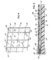
- the disclosed embodiment of the invention employs a multilayer thin film structure of the type depicted in FIGURE 2, which illustrates a portion of backplate 12 and conductive coating 14.
- the first layer 40 is a material such as titanium dioxide or tin-indium oxide that substantially improves the adherence of a second layer 42 of a highly conductive metal such as gold, silver, platinum or palladium.
- the surface layer 44 forms the relatively durable surface of the conductive coatings 14 (and 30) and is formed of tin-indium oxide.
- the exact conductance of a multilayer thin film structure cannot be theoretically predicted, but depends on a number of factors such as the conductivities of the various materials employed, the solid solution and multiphase alloying characteristics of such materials, the type of thin film deposition techniques employed (e.g., evaporation, plating, or sputtering) and, even when limited to sputtered films, depends on a system parameter such as the sputtering atmosphere, energy of the sputtered particles and the surface characteristics of the substrate material.
- optical properties e.g., transparency or transmissibility
- selection of the most advantageous conductive coating 14 and 30 often requires a certain amount of empirical testing to determine the thickness of each of the layers 40, 42 and 44 and, in some cases, on which material (gold, silver, platinum or palladium) is best used as the highly conductive second layer 42.
- conductive coatings 14 and 30 are often selected to achieve the desired optical filtering characteristics.
- conductive coatings 14 and 30 ideally result in a relatively high opacity of switch array 10 for spectra of a wavelength greater than that exhibited by the luminescent display characters and result in a high level of transparency for radiation emitted by the luminescent display.
- the first layer 40 consists of approximately 70-200 angstroms of titanium dioxide; the second layer 42 consists of approximately 40-150 angstroms of gold and the tin-indium oxide surface layer 44 is approximately 100-200 angstroms thick.
- silver, platinum or palladium would be considered for use as the highly conductive second layer 42 and experiments would be conducted to determine the optimal thickness range for each layer of the coatings 14 and 30.
- electrical contact to each conductive strip 16 of backplate 12 and each conductive strip 32 of plianrsheet 28 of the depicted embodiment of the transparent switch array 10 is provided by a thin, flat electrical cable assembly 48.
- electrical cable 48 is routed along the vertically-extending border region of backplate 12 that includes rectangular contact regions 22 and is routed along the lower boundary.of backplate 12 so as to be juxtaposed with the lower horizontal border region and contact regions 36 of pliant sheet 28 when the pliant sheet 28 is positoned in front of and spaced apart from backplate 12 in the manner depicted in FIGURE 1.
- electrical cable assembly 48 includes a relatively thin, flexible substrate tayer50 that is formed of a plastic material such as polyester film or a polyimide sheet material
- Parallel, spaced apart electrical conductors 52 run along one surface of the substrate 50 with a conductor being provided for each row element included on backplate 12-and each column element included on pliant sheet 28.
- a plurality of rectangular contacts 56 that substantially correspond in geometry and spacing with backplate contacts 22 and pliant sheet contacts 36 are formed on the second planar surface of cable substrate 50. More specifically, the cable contacts 56.
- each cable contact region 56 preferably includes a gold surface layer 60 that ensures a reliable electrical contact with the associated contact region 22 or 36.
- interconnection between each cable contact region 56 and an associated one of the electrical cable conductors 52 is effected by, for example, a "plated-through hole" 62 that extends between the oppositely disposed surfaces of cable substrate 50.
- a thin transparent strip 64 having an adhesive material coated on both planar surfaces thereof, is routed along the surface of electrical cable assembly 48 that does not include the conductive contact regions 56.
- the adhesive strip 64 attaches cable assembly 48 to the lower border region of backplate 12 and loosely bonds the vertically extending portion of cable assembly 48 to one vertical border region of pliant sheet 28. Since the adhesive strip 64 is also used to fasten pliant sheet 28 to backplate 12 along vertical and horizontal regions that do not include electrical cable assembly 48, it can be recognized that the spacing between the juxtaposed backplate 12 and the pliant sheet 28 is not uniform around the entire periphery of switch array 10.
- the presently preferred embodiments of the invention employ a cable assembly 48 that is' approximately three mils (75 microns) thick with the adhesive strip 64 being approximately 1-1/2 mils (38 microns) thick. Because of the above-described folded configuration of electrical cable 48, the spacing between the conductive surface of backplate 12 and the conductive surface of pliant sheet 28 of such an embodiment may be on the order of seven to eight mils in the corner region of switch array 10 that includes the folded portion of electrical cable 48.
- portions of the switch array border regions that extend outwardly from the folded portion of electrical cable 48 will typically exhibit a backplate-compliant sheet spacing of approximately 4 to 6 mils (100 to 150 microns) and the backplate-compliant sheet spacing along the border regions 24 and 38 that are separated only by the adhesive strip 64 is typically on the order of 1-1/2 to 2 mils (37 to 50 microns).
- backplate 12 could be employed to provide more uniform peripheral spacing between pliant sheet 28 and backplate 12, such measures do not appreciably improve either the structural integrity or the operation.
- the two most important criteria are that the conductive regions of backplate 12 and pliant sheet 28 do not contact one another unless pliant sheet 28 is deformed by pressing it toward backplate 12 and that a region of pliant sheet 28 that contains a conductive strip 32 and is urged into contact with the conductive surface of backplate 12 contacts only the oppositely disposed conductive strip 16 of backplate 12.
- the conductive surface of pliant sheet 28 includes an array of small transparent beads or "dots" 66 that are somewhat hemispherical in shape.
- the presently preferred embodiments of the invention include four dots that are deposited on the surface of pliant sheet 28-and form a substantially symmetric pattern about the intersection between a gap 34 that separates the conductive strips 32 of pliant sheet 28 and a gap 20 of backplate 12.
- each gap 34 of pliant sheet 28 includes a series of spaced apart dots 66 wherein each pair of consecutive dots are substantially equidistant from an orthogonal trace 68 that aligns with a gap 20 of backplate 12 when the switch array is assembled in the manner depicted in FIGURE 1.
- an additional series of dots is formed on each trace 68 that extends across the conductive surface of pliant sheet 28, with each pair of consecutive dots along a trace 68 being positioned so that each dot thereof lies on trace 68 and is substantially equidistant from two dots that are deposited in a gap 34.
- the above-discussed dot pattern of the presently preferred embodiments in effect, defines a matrix of rectangular touch regions 70 wherein the periphery of each touch region includes eight dots 66 (two per side).
- the dots 66 are approximately 0.8 to 1.25 mils in diameter (20 to 32 microns) and project outwardly from the surface of pliant sheet 28 to as to maintain a backplate to pliant sheet spacing of approximately 0.8 to 1.25 mils (20 to 32 microns).
- an organo-silicon based elastomer is applied to the surface of pliant sheet 28 by means of a silk-screen (not shown in the drawing) which includes open weave areas that define the desired geometric dot pattern.
- the material utilized should cure at a relatively low temperature (e.g., room temperature) to form flexible transparent beads or dots and should be selected for satisfactory adherence to both the conductive coating 30 and the gap regions 34 of pliant sheet 28.
- a relatively low temperature e.g., room temperature
- the diffraction coefficient of the organo-silicon elastomer should be substantially equal to the square root of the diffraction coefficient of pliant sheet 28.
- One material that has proven satisfactory in the practice of this invention is an organo-silicon material that is marketed by Dow Corning Corporation of Midland, Michigan under the product identification DC3440. In utilzing this material sufficient xylene is added to produce the paste- like consistency required for optimum silk-screening. Although solvents other than xylene may be satisfactory, it has been found that the xylene acts as somewhat of an etchant relative to the polyester film utilized to fabricate pliant sheet 28 and thereby improves the bond between pliant sheet 28 and the dots 66. Moreover, xylene appears to increase the air cure time of the elastomer being employed, thereby improving the "pot-life" of the material and permitting batch processing techniques to be employed.
- the pliant sheet 28 is assembled to backplate 12 without the use of conventional fasteners or permanent bonding techniques and the contact regions 56 of cable assembly 48 are not soldered or otherwise joined to the abutting backplate contact regions 22 and pliant sheet contact regions 36.
- the surface of electrical cable assembly 48 which is oppositely disposed to the surface that includes the contact regions 56 is affixed to the facing regions of backplate 12 and pliant sheet 28 only by means of adhesive strip 64.
- a series of U-shaped spring clips 72 preferably formed of metal strip material of a width that is commensurate-with the width of the rectangular contact regions 22, 32 and 56, are installed along the periphery of the switching array to maintain the components in the proper orientation and to ensure satisfactory electrical contact between electrical cable 48 and the conductive row and column elements of backplate 12 and pliant sheet 28.
- a spring clip 72 is placed over each edge region of switch array 10 that includes a pair of the contacts 22, 32 and 56 to, as is shown in FIGURE 5, exert compressive force that urges the contact regions against one another so as to maintain satisfactory electrical contact. Additional spring clips 72 are spaced along the remaining periphery of the switch array 10 as is required to secure pliant sheet 28 to backplate 12.
- a sheet of thermoplastic material of the desired type is placed on a mold having a surface contour that corresponds to the desired contour of backplate 12 (i.e., the curvature of the face of the associated cathode-ray tube 26 in FIGURE 1).
- the mold and the sheet material are then placed in an infrared oven and heated to a temperature at which backplate 12 assumes the curvature of the mold.
- Backplate 12 is then cleaned and a uniform coating of the previously-described type is deposited on one entire surface of the backplate by successive vacuum depositing (sputtering) of, for example, titanium dioxide, gold and tin-indium oxide of the previously-mentioned thicknesses.
- the thicker gold that defines the above-described backplate contact regions is then formed by continued sputtering or other low temperatue deposition techniques.
- the conductive coating of pliant sheet 28 is formed in the same manner, without the necessity of molding the polyester film or other material employed to match the curvature of backplate 12 and the associated cathode-ray tube 26.
- the conductive rows of backplate 12 and the conductive columns of pliant sheet 28 are then formed by placing the coating surfaces of backplate 12 and pliant sheet 28 against an array of thin, parallel wires. An electrical current is introduced in the wires so that the wires attain a temperature that removes the conductive coating from the contacting regions of backplate 12 and pliant sheet 28.
- other methods such as scribing can be employed to form the backplate gaps 20 and pliant sheet gaps 34 that define conductive strips 16 and 32 of backplate 12 and pliant sheet 28, the above-mentioned method produces very thin gaps that are relatively indiscernible.
- the backplate 12, pliant sheet 28 and electrical cable 48 are then assembled in the manner discussed relative to FIGURE 1 and the U-shaped spring clips 72 are installed.
- embodiments that utilize relatively large conductive strips to form larger touch-pressure activated switches than those of the discussed embodiments may require the use of a dot pattern that includes additional dots 66 to prevent inadvertent contact between the conductive regions of the backplate and the pliant sheet.
Landscapes
- Push-Button Switches (AREA)
Claims (11)
Applications Claiming Priority (2)
| Application Number | Priority Date | Filing Date | Title |
|---|---|---|---|
| US255677 | 1981-04-20 | ||
| US06/255,677 US4423299A (en) | 1981-04-20 | 1981-04-20 | Touch sensitive transparent switch array |
Publications (2)
| Publication Number | Publication Date |
|---|---|
| EP0063851A1 EP0063851A1 (fr) | 1982-11-03 |
| EP0063851B1 true EP0063851B1 (fr) | 1986-07-30 |
Family
ID=22969413
Family Applications (1)
| Application Number | Title | Priority Date | Filing Date |
|---|---|---|---|
| EP82300075A Expired EP0063851B1 (fr) | 1981-04-20 | 1982-01-07 | Clavier à interrupteurs transparent |
Country Status (4)
| Country | Link |
|---|---|
| US (1) | US4423299A (fr) |
| EP (1) | EP0063851B1 (fr) |
| JP (1) | JPS57180819A (fr) |
| DE (1) | DE3272227D1 (fr) |
Families Citing this family (31)
| Publication number | Priority date | Publication date | Assignee | Title |
|---|---|---|---|---|
| JPS58142715A (ja) * | 1982-02-17 | 1983-08-24 | キヤノン株式会社 | キ−ボ−ド |
| JPS5998408A (ja) * | 1982-11-29 | 1984-06-06 | 横浜ゴム株式会社 | 感圧型導電性複合シ−ト |
| JPS6032214A (ja) * | 1983-08-02 | 1985-02-19 | キヤノン株式会社 | キ−ボ−ド |
| US4598472A (en) * | 1983-08-19 | 1986-07-08 | Amp Incorporated | Method for forming a hemispherically shaped switch assembly |
| US4594482A (en) * | 1984-01-23 | 1986-06-10 | Canon Kabushiki Kaisha | Input element with improved appearance and reliability |
| JPS6168422U (fr) * | 1984-10-11 | 1986-05-10 | ||
| US4725696A (en) * | 1985-06-11 | 1988-02-16 | Shin-Etsu Polymer Co., Ltd. | Touch-operated see-through coordinate input unit |
| US4965421A (en) * | 1985-09-26 | 1990-10-23 | John Fluke Mfg. Co., Inc. | Particulate spacers for touch sensitive overlay panel applications |
| CN1010143B (zh) * | 1985-09-26 | 1990-10-24 | 约翰弗兰克制造公司 | 供触敏涂覆层使用的粒子垫片 |
| US4696860A (en) * | 1985-09-26 | 1987-09-29 | John Fluke Mfg. Co., Inc. | Particulate spacers for inhibiting Newton rings in touch sensitive overlays |
| USRE38419E1 (en) | 1986-05-13 | 2004-02-10 | Ncr Corporation | Computer interface device |
| US4959805A (en) * | 1987-03-17 | 1990-09-25 | Alps Electric Co., Ltd. | Coordinate detecting device |
| US4786767A (en) * | 1987-06-01 | 1988-11-22 | Southwall Technologies Inc. | Transparent touch panel switch |
| DE8714217U1 (de) * | 1987-10-26 | 1987-12-23 | Preh, Elektrofeinmechanische Werke Jakob Preh Nachf. Gmbh & Co, 8740 Bad Neustadt | Tastenkappe für eine Tastatur |
| US4931782A (en) * | 1988-06-24 | 1990-06-05 | E. I. Du Pont De Nemours And Company | Touch screen overlay with improved conductor durability |
| DE3914984A1 (de) * | 1989-05-06 | 1990-11-08 | Licentia Gmbh | Tastatur fuer eine datenverarbeitungseinrichtung |
| GB2233499B (en) * | 1989-06-28 | 1994-03-02 | Mitsubishi Electric Corp | Sheet-like switch |
| JP2598152B2 (ja) * | 1990-04-28 | 1997-04-09 | シャープ株式会社 | タッチパネル |
| DE9012407U1 (de) * | 1990-08-30 | 1992-01-09 | Platz, Karl Otto, 5226 Reichshof | Druckschaltelement |
| US5228562A (en) * | 1991-09-09 | 1993-07-20 | Gm Nameplate, Inc. | Membrane switch and fabrication method |
| DE4134358A1 (de) * | 1991-10-17 | 1993-04-22 | Standard Elektrik Lorenz Ag | Schaltungseinrichtung zur abfrage einer tastatur |
| DE19923392C1 (de) * | 1999-05-21 | 2001-02-01 | Ackermann Albert Gmbh Co | Hand-Bediengerät für den Pflegebereich |
| US6305073B1 (en) | 1999-12-29 | 2001-10-23 | Gm Nameplate, Inc. | One-sided electrode arrangement on an intermediate spacer for a touchscreen |
| JP2002222055A (ja) * | 2001-01-26 | 2002-08-09 | Matsushita Electric Ind Co Ltd | タッチパネル |
| US6906273B2 (en) * | 2002-08-09 | 2005-06-14 | Stoneridge Control Devices, Inc. | Switch assembly |
| US7706046B2 (en) | 2004-06-08 | 2010-04-27 | Gentex Corporation | Rearview mirror element having a circuit mounted to the rear surface of the element |
| TWI466004B (zh) | 2009-04-17 | 2014-12-21 | Egalax Empia Technology Inc | 電阻式多點觸控裝置及方法 |
| MX2013011886A (es) | 2011-04-13 | 2014-03-31 | Kior Inc | Catalizador mejorado para conversion termocatalitica de biomasa para combustibles liquidos y productos quimicos. |
| US9518229B2 (en) | 2012-07-20 | 2016-12-13 | Inaeris Technologies, Llc | Catalysts for thermo-catalytic conversion of biomass, and methods of making and using |
| US9522392B2 (en) | 2013-03-15 | 2016-12-20 | Inaeris Technologies, Llc | Phosphorous promotion of zeolite-containing catalysts |
| CN110010397A (zh) * | 2019-05-15 | 2019-07-12 | 光宝电子(广州)有限公司 | 发光按键 |
Family Cites Families (11)
| Publication number | Priority date | Publication date | Assignee | Title |
|---|---|---|---|---|
| US3594684A (en) * | 1969-05-12 | 1971-07-20 | Datanetics Corp | Electrical interconnection system for multilayer circuitry |
| FR2268342A1 (en) | 1974-04-19 | 1975-11-14 | Ducros Emile | Touch operated electric switch - has moving contact grid covered in insulating material sheet and fixed contacts |
| US4017848A (en) * | 1975-05-19 | 1977-04-12 | Rockwell International Corporation | Transparent keyboard switch and array |
| US4017697A (en) | 1975-09-15 | 1977-04-12 | Globe-Union Inc. | Keyboard membrane switch having threshold force structure |
| US4145584A (en) * | 1976-04-28 | 1979-03-20 | Otterlei Jon L | Flexible keyboard switch with integral spacer protrusions |
| US4071718A (en) * | 1976-10-22 | 1978-01-31 | Bowmar Instrument Corporation | Flat keyboard assembly having cover type membrane with protrusions to align switch components |
| US4085302A (en) * | 1976-11-22 | 1978-04-18 | Control Data Corporation | Membrane-type touch panel |
| US4143253A (en) | 1977-04-25 | 1979-03-06 | Amp Incorporated | Optically clear membrane switch |
| US4220815B1 (en) * | 1978-12-04 | 1996-09-03 | Elographics Inc | Nonplanar transparent electrographic sensor |
| US4243852A (en) * | 1979-04-16 | 1981-01-06 | Oak Industries Inc. | Membrane switch with means for impeding silver migration |
| JPS55143722A (en) * | 1979-04-26 | 1980-11-10 | Nissan Motor | Switching device |
-
1981
- 1981-04-20 US US06/255,677 patent/US4423299A/en not_active Expired - Lifetime
-
1982
- 1982-01-07 EP EP82300075A patent/EP0063851B1/fr not_active Expired
- 1982-01-07 DE DE8282300075T patent/DE3272227D1/de not_active Expired
- 1982-03-29 JP JP57049228A patent/JPS57180819A/ja active Pending
Also Published As
| Publication number | Publication date |
|---|---|
| JPS57180819A (en) | 1982-11-08 |
| EP0063851A1 (fr) | 1982-11-03 |
| US4423299A (en) | 1983-12-27 |
| DE3272227D1 (en) | 1986-09-04 |
Similar Documents
| Publication | Publication Date | Title |
|---|---|---|
| EP0063851B1 (fr) | Clavier à interrupteurs transparent | |
| CA1047082A (fr) | Commutateur a membrane | |
| US4085302A (en) | Membrane-type touch panel | |
| US4516112A (en) | Transparent touch switching system | |
| US5062198A (en) | Method of making a transparent touch screen switch assembly | |
| US4317011A (en) | Membrane touch switch | |
| US4066855A (en) | Vented membrane-type touch panel | |
| US4431882A (en) | Transparent capacitance membrane switch | |
| US5228562A (en) | Membrane switch and fabrication method | |
| US4220815A (en) | Nonplanar transparent electrographic sensor | |
| US7071927B2 (en) | Resistive touch panel using removable, tensioned top layer | |
| US6305073B1 (en) | One-sided electrode arrangement on an intermediate spacer for a touchscreen | |
| EP0614561B1 (fr) | Ecran tactile a dispositif d'espacement isole ameliore | |
| US3742279A (en) | Segmented electrode display panel having closed structure | |
| US3988551A (en) | Membrane keyboard apparatus having common apertured electrode, aperture inserted electrodes and conductive bubble contactors | |
| JP2916260B2 (ja) | 電気泳動表示装置およびその製造方法 | |
| US3877790A (en) | Large liquid crystal displays and method of producing them | |
| JPS61208533A (ja) | グラフイツクタツチセンサ | |
| CA1039838A (fr) | Panneau d'affichage a commande eletrostatique | |
| JPS6222135A (ja) | 透明図形入力タブレツト | |
| US4488084A (en) | Electroluminescence structure | |
| US4736190A (en) | Sheet membrane keyboard and electronic apparatus using same | |
| GB2177260A (en) | Touch-operated see-through coordinate input unit | |
| US4035061A (en) | Honeycomb display devices | |
| US4066853A (en) | Membrane type touch panel employing piezoresistant anti-short means |
Legal Events
| Date | Code | Title | Description |
|---|---|---|---|
| PUAI | Public reference made under article 153(3) epc to a published international application that has entered the european phase |
Free format text: ORIGINAL CODE: 0009012 |
|
| AK | Designated contracting states |
Designated state(s): DE FR GB NL |
|
| 17P | Request for examination filed |
Effective date: 19830415 |
|
| GRAA | (expected) grant |
Free format text: ORIGINAL CODE: 0009210 |
|
| AK | Designated contracting states |
Kind code of ref document: B1 Designated state(s): DE FR GB NL |
|
| REF | Corresponds to: |
Ref document number: 3272227 Country of ref document: DE Date of ref document: 19860904 |
|
| ET | Fr: translation filed | ||
| PGFP | Annual fee paid to national office [announced via postgrant information from national office to epo] |
Ref country code: NL Payment date: 19870131 Year of fee payment: 6 |
|
| PLBE | No opposition filed within time limit |
Free format text: ORIGINAL CODE: 0009261 |
|
| STAA | Information on the status of an ep patent application or granted ep patent |
Free format text: STATUS: NO OPPOSITION FILED WITHIN TIME LIMIT |
|
| 26N | No opposition filed | ||
| PG25 | Lapsed in a contracting state [announced via postgrant information from national office to epo] |
Ref country code: NL Effective date: 19890801 |
|
| NLV4 | Nl: lapsed or anulled due to non-payment of the annual fee | ||
| PG25 | Lapsed in a contracting state [announced via postgrant information from national office to epo] |
Ref country code: FR Free format text: LAPSE BECAUSE OF NON-PAYMENT OF DUE FEES Effective date: 19890929 |
|
| REG | Reference to a national code |
Ref country code: FR Ref legal event code: ST |
|
| PGFP | Annual fee paid to national office [announced via postgrant information from national office to epo] |
Ref country code: GB Payment date: 19951228 Year of fee payment: 15 |
|
| PG25 | Lapsed in a contracting state [announced via postgrant information from national office to epo] |
Ref country code: GB Effective date: 19970107 |
|
| GBPC | Gb: european patent ceased through non-payment of renewal fee |
Effective date: 19970107 |
|
| PGFP | Annual fee paid to national office [announced via postgrant information from national office to epo] |
Ref country code: DE Payment date: 20010126 Year of fee payment: 20 |