EP0063886B1 - Procédé et système de communication par impulsions - Google Patents
Procédé et système de communication par impulsions Download PDFInfo
- Publication number
- EP0063886B1 EP0063886B1 EP82301861A EP82301861A EP0063886B1 EP 0063886 B1 EP0063886 B1 EP 0063886B1 EP 82301861 A EP82301861 A EP 82301861A EP 82301861 A EP82301861 A EP 82301861A EP 0063886 B1 EP0063886 B1 EP 0063886B1
- Authority
- EP
- European Patent Office
- Prior art keywords
- signal
- mark inversion
- coded mark
- level
- transmission
- Prior art date
- Legal status (The legal status is an assumption and is not a legal conclusion. Google has not performed a legal analysis and makes no representation as to the accuracy of the status listed.)
- Expired
Links
- 238000004891 communication Methods 0.000 title claims description 30
- 238000000034 method Methods 0.000 title claims description 9
- 230000005540 biological transmission Effects 0.000 claims description 98
- 230000008054 signal transmission Effects 0.000 claims description 19
- 230000003287 optical effect Effects 0.000 claims description 11
- 238000012544 monitoring process Methods 0.000 claims description 10
- 239000013307 optical fiber Substances 0.000 claims description 3
- 230000001172 regenerating effect Effects 0.000 claims description 3
- 238000010586 diagram Methods 0.000 description 9
- 230000005856 abnormality Effects 0.000 description 6
- 230000000630 rising effect Effects 0.000 description 6
- 238000006243 chemical reaction Methods 0.000 description 3
- 239000000284 extract Substances 0.000 description 2
- 239000000835 fiber Substances 0.000 description 2
- 230000000052 comparative effect Effects 0.000 description 1
- 238000010276 construction Methods 0.000 description 1
- 238000004377 microelectronic Methods 0.000 description 1
- 230000003252 repetitive effect Effects 0.000 description 1
Images


Classifications
-
- H—ELECTRICITY
- H04—ELECTRIC COMMUNICATION TECHNIQUE
- H04L—TRANSMISSION OF DIGITAL INFORMATION, e.g. TELEGRAPHIC COMMUNICATION
- H04L25/00—Baseband systems
- H04L25/38—Synchronous or start-stop systems, e.g. for Baudot code
- H04L25/40—Transmitting circuits; Receiving circuits
- H04L25/49—Transmitting circuits; Receiving circuits using code conversion at the transmitter; using predistortion; using insertion of idle bits for obtaining a desired frequency spectrum; using three or more amplitude levels ; Baseband coding techniques specific to data transmission systems
- H04L25/4906—Transmitting circuits; Receiving circuits using code conversion at the transmitter; using predistortion; using insertion of idle bits for obtaining a desired frequency spectrum; using three or more amplitude levels ; Baseband coding techniques specific to data transmission systems using binary codes
- H04L25/4908—Transmitting circuits; Receiving circuits using code conversion at the transmitter; using predistortion; using insertion of idle bits for obtaining a desired frequency spectrum; using three or more amplitude levels ; Baseband coding techniques specific to data transmission systems using binary codes using mBnB codes
- H04L25/491—Transmitting circuits; Receiving circuits using code conversion at the transmitter; using predistortion; using insertion of idle bits for obtaining a desired frequency spectrum; using three or more amplitude levels ; Baseband coding techniques specific to data transmission systems using binary codes using mBnB codes using 1B2B codes
- H04L25/4912—Transmitting circuits; Receiving circuits using code conversion at the transmitter; using predistortion; using insertion of idle bits for obtaining a desired frequency spectrum; using three or more amplitude levels ; Baseband coding techniques specific to data transmission systems using binary codes using mBnB codes using 1B2B codes using CMI or 2-HDB-3 code
Definitions
- the present invention relates to a method of and a system for pulse communication which has a large signal transmission speed and a large transmission capacity and which permits the signal transmission line to be monitored.
- Such a method and system is particularly suitable for communication by the transmission of optical pulses along optical fibres.
- the Auffret article also discusses an encoding system referred to as HDB in which a binary code is converted into a ternary or 3-level HDB code.
- Another article referring to the use of a 3-level code is by Hanson entitled "Integrated Components for Fibre Optic Data Links in Industrial Applications” from Microelectronics and Reliability, Volume 18 numbers 1/2 (1978), pages 175 to 178.
- data is transmitted by generating a positive going pulse at the conversion point between a data 1 and a data 0 and a negative going pulse at a conversion point between a data 0 and a data 1.
- the 2-level coded mark inversion code is converted into a 3-level signal before it is transmitted through a transmission line from a transmission site to a reception site and then, at the reception site the 3-level signal is initially converted into a 2-level coded mark inversion code before the data signal and clock signal are separately recovered.
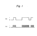
- Figure 1 illustrates the principle of a previously used pulse communication system.
- the previously known pulse communication system operated as a 2-level pulse communication system in which data signals were transmitted as logical 0 and 1 as shown in Figure 1(a), or were transmitted as envelope modulations in a pulse communication system in which repetition pulses were subjected to envelope modulation as shown in Figure 1 (b).
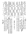
- Fig. 2 shows the principle of the pulse communication method according to the present invention, in which a transmission data signal (a) is converted into a coded mark inversion (CMI) code (c) and thereafter modulated into a 3-level CMI signal (g) and transmitted by the signal transmission line. On the reception side, the received signal is demodulated separately into the data signal and the clock signal.
- 01 of the CMI code (c) is corresponded to logical 1 of the transmission data signal (a) and 11 or 00 of the CMI code (c) is corresponded to logical 0 of the transmission data signal (a) while 10 of the CMI code (c) is not corresponded to any of logical 1 and 0 of the transmission data signal (a).
- 00 and 11 of the CMI code (c) are alternately corresponded to logical 0 of the transmission data signal (a).
- the transmission data signal (a) of frequency fo is sampled at the middle of the signal frequency in synchronism with the rising of the transmission clock signal (b) of frequency 2fo and is converted into the transmission CMI code (c) in accordance with the correspondance described above.
- the transmission CMI code (c) since 00 of the transmission CMI code (c) is corresponded to the first transmission data signal 0, 11 and 00 are alternatively repeatedly corresponded to logical 0 of the further transmission data signal (a).
- the transmission CMI code (c) is converted in synchronism with the rising of a transmission multiplied clock signal (d) of frequency 4fo into the 3-level CMI signal (g) to logical 0 and -1 of which logical 1 and 0 of the transmission CMI code are corresponded.
- logical 1 of the transmission data signal (a) is converted into one negative pulse and one positive pulse of the 3-level CMI signal (g) in correspondence with the falling and the rising, respectively, of the transmission clock signal.
- logical 0 of the transmission data signal (a) is converted into two positive pulses or two negative pulses of the 3-level CMI signal (g) in correspondence with the falling and the rising, respectively, of the transmission clock signal.
- the two positive or negative pulses of the 3-level CMI signal (g) are pulse signals having the signs opposite to two pulse signals used for logical 0 of the transmission data signal (a) immediately before them.
- This 3-level CMI signal is transmitted to the reception side through the signal transmission line.
- the probability of occurrence of logical 0 and 1 in the 3-level CMI signal (g) as a whole is 1:1.
- the average value of the 3-level CMI signal (g) is half of the peak value (in Fig. 2, it is the half of the maximum value +1 and the minimum value -1, that is 0), to make the level of the transmission signal easily detectable. This characteristic can be utilized as an abnormality monitoring signal of the signal transmission line.
- the abnormality can be detected by comparing the half value level with the predetermined reference value by means of a comparator.
- This characteristic of the system according to the present invention is effective particularly in the optical pulse communication system in which the signal is transmitted by the optical pulse in the optical fiber. Further, since both the positive pulse and the negative pulse of the 3-level CMI signal (g) are corresponded to the rising or the falling of the transmission clock signal (b) and since 10 of the transmission CMI code (c) is not corresponded to any of logical 0 and 1 of the transmission data signal (a), it can be distinguished whether the pulse of the 3-level CMI signal corresponds to the rising or to the falling of the clock signal.
- the pulse communication system can transmit the clock signal with the data signal.
- the transmission data signal (a) can be demodulated to a reception data signal through reverse steps to the transmission, by corresponding logical 1 of the reception data signal to 01 of the reception CMI code (c) and corresponding logical 0 of the reception data signal to 00 or 11 of the reception CMI code (c).
- the 3-level CMI signal to be transmitted includes the data signal, the clock signal, and the transmission line monitoring signal.
- the necessary transmission band is only four times the signal pulse frequency. That is, one fourth of the transmission band can be used as the data signal.
- the reception timing clock signal corresponding to the reception data signal can be easily extracted by a sequence circuit operated with the clock signal four times the transmission speed without using any complicated circuit such as PLL circuit.
- the reception data signal includes clock information including phase, and the clock information can be easily regenerated by the sequential circuit transiting in the clock frequency twice the transmission speed. Since 10 of the CMI code is not used as data, another advantage is provided that even if the phase of the clock is shifted 180 degrees with respect to the data signal, it can be corrected.
- the positive pulse is corresponded to logical 1 and the negative pulse is corresponded to logical 0, they may be otherwise corresponded, for example, the negative pulse is corresponded to logical 1 and the positive pulse is corresponded to logical 0.
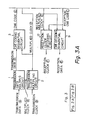
- Figs. 3A and 3B are a block diagram showing a pulse communication system for practising the pulse communication system according to the present invention, comprising a transmission data holding circuit 1, a transmission clock multiplying circuit 2, a CMI coding sequential circuit 3, a modulating circuit 4, a 3-level CMI signal coding circuit 5, a signal transmission line 6, a 3-level CMI signal decoding circuit 7, a demodulating circuit 8, a CMI decoding sequential circuit 9, a transmission line monitoring circuit 10, a multiplied clock regenerating circuit 11, and a reception clock decoding sequential circuit 12.
- the transmission clock multiplying circuit 2 converts the transmission clock signal (b) into the transmission multiplied clock signal (d) of frequency 4fo which is twice the frequency 2fo and applies the transmission multipled clock signal (d) to the transmission data holding circuit 1, the CMI coding sequential circuit 3 and the modulating circuit 4.
- the CMI coding sequential circuit 3 converts the transmission data signal (a) into the transmission CMI code (c).
- the modulating circuit 4 separates the transmission CMI code (c) into the transmission positive pulse signal (d) and the transmission negative pulse signal (e) which are converted into the 3-level CMI signal (g) by the 3-level CMI signal coding circuit 5.
- the 3-level CMI signal (g) is transmitted as an optical signal by a light emitting diode of the 3-level CMI signal coding circuit 5 through the signal transmission line 6 comprising the optical fibers.
- the 3-level CMI signal decoding circuit 7 decodes the 3-level CMI signal of the optical signal into the electrical reception positive pulse signal (A) and reception negative pulse (B) which are demodulated into the reception CMI code (C) by the demodulating circuit 8.
- the multiplication clock regenerating circuit 11 extracts the reception multiplied clock signal (D) from the 3-level CMI signal (g) and applies it to the CMI decoding sequential circuit 9 which converts the reception CMI code (c) into the reception data signal (E) and reception clock decoding circuit 12.
- the reception clock decoding sequential circuit 12 converts the reception CMI code (C) into the reception clock signal (F) by the reception multiplied clock signal. By this, the data signal and the clock signal are extracted separately.
- the 3-level CMI signal decoding circuit 7 takes out the average value of the 3-level CMI signal which is the optical signal received thereby, and the transmission line monitoring circuit 10 outputs a transmission line monitoring signal for monitoring the abnormality of the signal transmission line by comparing always the average value with a predetermined value.
- Fig. 4 shows an embodiment of the CMI coding sequential circuit 3 according to the present invention, in which reference numerals 13a and 13b denote data holding flip-flops, and reference numerals 14a and 14b denote JK input type flip-flops.
- the flip-flop 13b holds the transmission data signal (a) by the transmission multiplied clock signal (d)
- the flip-flop 13a holds the transmission data signals (a) sequentially with one clock's delay from the flip-flop 13b by the transmission multiplied clock signal (d).
- the outputs of the flip-flops 13a, 13b, 14a and 14b are returned to the JK inputs of the flip-flops 14a and 14b by a combinational circuit to form the CMI coding sequential circuit 3.
- Fig. 5 shows an embodiment of the modulating circuit 4 according to the present invention, in which the transmission CMI code (c) is applied to a 2-input NAND gate 16a and inverted by an inverter 17a into the transmission positive pulse signal (e).
- the transmission CMI code (c) inverted by an inverter 15 is applied to a 2-input NAND gate 16b and isfurther inverted by an inverter 17b into the transmission negative pulse signal (f).
- Fig. 6 shows an embodiment of the 3-level CMI signal coding circuit 5 according to the present invention, in which the transmission positive pulse signal (e) and the transmission negative pulse signal (f) are applied to one inputs of 2-input NAND gates 18a and 18b, respectively, and transmission control signals are applied to the other inputs thereof.
- the transmission control signal to decide whether the optical signal is or is not to be transmitted. If the data signal is to be transmitted, the transmission control signal becomes logical 1, and a light emitting diode 19 emits light at the maximum value when the transmission positive pulse signal (e) is applied and at the minimum value when the transmission negative pulse signal (f) is applied.
- the transmission control signal In the state where the transmission control signal is logical 1 and yet there is no transmission signal pulse, the light emitting diode 19 emits light at the half value of the maximum value and the minimum value determined by resistors 20 and 21. If the data signal is not to be transmitted, the transmission control signal becomes logical 0 and the light emitting diode 19 is extinguished.
- the transmission data signal (a) is transmitted by the diode 19 as an optical pulse signal carried through the signal transmission line 6, it will be obvious to those skilled in the art that another embodiment of the 3-level CMI signal coding circuit 5 for carrying an ordinary electrical pulse signal is easily constructed within the scope of the present invention.
- Fig. 7 shows an embodiment of the 3-level CMI signal decoding circuit 7, in which the 3-level CMI signal (g) transmitted through the signal transmission line 6 is amplified by a preamplifier 22 and thereafter applied to a positive pulse comparator 24, a negative pulse comparator 25, and a threshold setting circuit 23 generates the half value of the maximum and the minimum value of the transmitted signal as a predetermined threshold value.
- the positive pulse comparator 24 outputs the reception positive pulse signal (A) when the 3-level CMI signal (g) is larger than the threshold value and, on the other hand, the negative pulse comparator 25 outputs the reception negative pulse signal (B) when the 3-level CMI signal (g) is smaller than the threshold value.
- the transmitted 3-level CMI signal (g) is applied also to a reception signal average extracting circuit 30 which extracts the average value of the received 3-level CMI signals (g).
- the average value is compared by a comparator 31 with a reference value outputted by a reception signal reference setting circuit 29 for distinguishing any abnormality in the signal transmission line, and the comparator 31 outputs a transmission line monitoring signal.
- Fig. 8 shows an embodiment each of the demodulating circuit 8 and the CMI decoding sequential circuit 9 according to the present invention.
- the demodulating circuit 8 is constructed as an RS flip-flop.
- the reception CMI code (C) which is the output signal of the RS flip-flop is held sequentially by the reception multiplied clock signal (D).
- the data holding flip-flop 27b holds the reception CMI code to the data holding flip-flop 27a one clock later than the reception multiplied clock signal (D).
- the CMI decoding sequential circuit 9 formed by returning the outputs of JK input flip-flop 28a and 28b and the outputs of the data holding flip-flops 27a and 27b to the inputs of the JK input flip-flops 28a and 28b by means of a combinational circuit makes, as shown in Fig. 2, the reception data signal (E) and the reception clock signal (F) from the reception positive pulse signal (A) and the reception negative pulse signal (B).
- a pulse communication system which is compact in construction and yet is large both in the signal transmission speed and in the transmission capacity, and further is capable of deciding easily whether absence of a signal pulse is due to any abnormality in the signal transmission line or due to one of the 2-level signal pulses, to thereby monitor the transmission line.
Landscapes
- Physics & Mathematics (AREA)
- Spectroscopy & Molecular Physics (AREA)
- Engineering & Computer Science (AREA)
- Computer Networks & Wireless Communication (AREA)
- Signal Processing (AREA)
- Dc Digital Transmission (AREA)
Claims (10)
caractérisé en ce qu'à l'étape de codage le code d'inversion de marque codée (c) est converti en un signal à 3 niveaux (g) avant transmission par la ligne de transmission et en ce qu'à l'étape de décodage le signal transmis à 3 niveaux (g) est initialement converti en un code d'inversion de marque codée à 2 niveaux (c).
Applications Claiming Priority (4)
| Application Number | Priority Date | Filing Date | Title |
|---|---|---|---|
| JP64898/81 | 1981-04-27 | ||
| JP56064898A JPS57178452A (en) | 1981-04-27 | 1981-04-27 | Optical communication system |
| JP34983/82 | 1982-03-05 | ||
| JP3498382A JPS58151753A (ja) | 1982-03-05 | 1982-03-05 | パルス通信方式 |
Publications (3)
| Publication Number | Publication Date |
|---|---|
| EP0063886A2 EP0063886A2 (fr) | 1982-11-03 |
| EP0063886A3 EP0063886A3 (en) | 1983-06-01 |
| EP0063886B1 true EP0063886B1 (fr) | 1985-12-18 |
Family
ID=26373861
Family Applications (1)
| Application Number | Title | Priority Date | Filing Date |
|---|---|---|---|
| EP82301861A Expired EP0063886B1 (fr) | 1981-04-27 | 1982-04-08 | Procédé et système de communication par impulsions |
Country Status (4)
| Country | Link |
|---|---|
| US (1) | US4442528A (fr) |
| EP (1) | EP0063886B1 (fr) |
| CA (1) | CA1187187A (fr) |
| DE (1) | DE3267979D1 (fr) |
Families Citing this family (16)
| Publication number | Priority date | Publication date | Assignee | Title |
|---|---|---|---|---|
| DE3245845A1 (de) * | 1982-12-10 | 1984-06-14 | Siemens AG, 1000 Berlin und 8000 München | Cmi-decoder |
| DE3468799D1 (en) * | 1983-11-17 | 1988-02-18 | Ant Nachrichtentech | Cmi coder |
| US4661801A (en) * | 1985-04-01 | 1987-04-28 | General Electric Company | Decoder for three level coded data |
| US4885582A (en) * | 1987-09-28 | 1989-12-05 | The Grass Valley Group, Inc. | "Simple code" encoder/decoder |
| US4860009A (en) * | 1988-02-12 | 1989-08-22 | Paradyne Corporation | Bidirectional multiframe converter for data communications systems |
| DE59008497D1 (de) * | 1989-04-20 | 1995-03-30 | Siemens Ag | Übertragungsstrecke. |
| JPH02312329A (ja) * | 1989-05-27 | 1990-12-27 | Fujitsu Ltd | 信号伝送方式 |
| KR920005364B1 (ko) * | 1989-12-12 | 1992-07-02 | 한국전기통신공사 | Nrz/cmi(ii) 부호 변환장치 |
| US5020872A (en) * | 1990-01-04 | 1991-06-04 | Smiths Industries Aerospace & Defense Systems Incorporated | Method of operating an electrooptic modulator |
| US5113187A (en) * | 1991-03-25 | 1992-05-12 | Nec America, Inc. | CMI encoder circuit |
| EP0589217A1 (fr) * | 1992-09-24 | 1994-03-30 | Siemens Stromberg-Carlson | Procédé et dispositif pour synchroniser des signaux transmis en série par une ligne |
| DE59713030D1 (de) * | 1996-07-24 | 2010-05-12 | Bosch Gmbh Robert | Verfahren zur synchronisierung von daten, schnittstelle zur übertragung |
| US6265971B1 (en) | 1999-04-09 | 2001-07-24 | Simplex Time Recorder Company | Fiber-sync communications channel |
| FI115864B (fi) * | 1999-09-06 | 2005-07-29 | Nokia Corp | Sarjamuotoinen rajapinta ja menetelmä digitaalisen datan siirtämiseksi sarjamuotoisen rajapinnan yli |
| US20020089726A1 (en) * | 2000-07-18 | 2002-07-11 | Zhan He | System and method for wavelength modulated free space optical communication |
| CN111913058A (zh) | 2020-06-18 | 2020-11-10 | 深圳麦克韦尔科技有限公司 | 气溶胶雾化设备、测试设备及其控制方法和控制装置 |
Family Cites Families (5)
| Publication number | Priority date | Publication date | Assignee | Title |
|---|---|---|---|---|
| GB1489177A (en) * | 1973-10-16 | 1977-10-19 | Gen Electric Co Ltd | Digital data signalling systems and apparatus therefor |
| GB1512700A (en) * | 1975-10-23 | 1978-06-01 | Standard Telephones Cables Ltd | Data transmission |
| US4083005A (en) * | 1976-11-01 | 1978-04-04 | Burroughs Corporation | Three-level serial digital data communication system |
| GB1563848A (en) * | 1977-02-09 | 1980-04-02 | Hewlett Packard Ltd | Cmi-encoder |
| NL7903103A (nl) * | 1979-04-20 | 1980-10-22 | Philips Nv | Transmissiestelsel voor de overdracht van tweewaardige datasymbolen. |
-
1982
- 1982-04-08 DE DE8282301861T patent/DE3267979D1/de not_active Expired
- 1982-04-08 CA CA000400788A patent/CA1187187A/fr not_active Expired
- 1982-04-08 EP EP82301861A patent/EP0063886B1/fr not_active Expired
- 1982-04-14 US US06/368,846 patent/US4442528A/en not_active Expired - Lifetime
Also Published As
| Publication number | Publication date |
|---|---|
| DE3267979D1 (en) | 1986-01-30 |
| CA1187187A (fr) | 1985-05-14 |
| EP0063886A3 (en) | 1983-06-01 |
| US4442528A (en) | 1984-04-10 |
| EP0063886A2 (fr) | 1982-11-03 |
Similar Documents
| Publication | Publication Date | Title |
|---|---|---|
| EP0063886B1 (fr) | Procédé et système de communication par impulsions | |
| EP0610204B1 (fr) | Code en ligne utilisant l'inversion de bloc pour des liaisons rapides | |
| US4530088A (en) | Group coding system for serial data transmission | |
| EP0595034B1 (fr) | Modulation d'impulsions en position codée différentielle avec du temps de garde pour réseaux de communications | |
| EP0040632B1 (fr) | Systeme de traitement de donnees avec transmission serielle de donnees entre des sous systemes | |
| CA1266128A (fr) | Interface de modulation de donnees | |
| US4347617A (en) | Asynchronous transmission system for binary-coded information | |
| CN1140086C (zh) | 数字数据串行传输的通信接口及其对应的数据传输方法 | |
| EP0124959A2 (fr) | Méthode de codage par groupe pour la transmission de données en série | |
| CA2043596C (fr) | Emetteur-recepteur optique | |
| US4740998A (en) | Clock recovery circuit and method | |
| Pollard | Multilevel data communication over optical fibre | |
| EP0089467B1 (fr) | Méthode et système pour la transmission de signaux d'impulsions | |
| EP0692887A1 (fr) | Dispositif de communication optique | |
| US4503472A (en) | Bipolar time modulated encoder/decoder system | |
| EP0786182B1 (fr) | Codage de signaux infrarouges | |
| Kawanishi et al. | DmB1M code and its performance in a very high-speed optical transmission system | |
| US5969839A (en) | Optical communications device | |
| EP0284164B1 (fr) | Unité de décodage pour des signaux à codage CMI | |
| EP0326614B1 (fr) | Decodeur de signaux synchrone | |
| US4928289A (en) | Apparatus and method for binary data transmission | |
| US4606056A (en) | Method of encoding and serially transmitting self-clocking data and control characters | |
| JPS61201534A (ja) | 衝突検出機能付き送受信装置 | |
| US4201884A (en) | Digital data transmission system | |
| EP0476968A2 (fr) | Système pour la récuperation de l'horloge |
Legal Events
| Date | Code | Title | Description |
|---|---|---|---|
| PUAI | Public reference made under article 153(3) epc to a published international application that has entered the european phase |
Free format text: ORIGINAL CODE: 0009012 |
|
| AK | Designated contracting states |
Designated state(s): DE FR GB |
|
| PUAL | Search report despatched |
Free format text: ORIGINAL CODE: 0009013 |
|
| AK | Designated contracting states |
Designated state(s): DE FR GB |
|
| 17P | Request for examination filed |
Effective date: 19831014 |
|
| GRAA | (expected) grant |
Free format text: ORIGINAL CODE: 0009210 |
|
| AK | Designated contracting states |
Designated state(s): DE FR GB |
|
| REF | Corresponds to: |
Ref document number: 3267979 Country of ref document: DE Date of ref document: 19860130 |
|
| ET | Fr: translation filed | ||
| PLBE | No opposition filed within time limit |
Free format text: ORIGINAL CODE: 0009261 |
|
| STAA | Information on the status of an ep patent application or granted ep patent |
Free format text: STATUS: NO OPPOSITION FILED WITHIN TIME LIMIT |
|
| 26N | No opposition filed | ||
| PGFP | Annual fee paid to national office [announced via postgrant information from national office to epo] |
Ref country code: GB Payment date: 19960401 Year of fee payment: 15 |
|
| PGFP | Annual fee paid to national office [announced via postgrant information from national office to epo] |
Ref country code: FR Payment date: 19960410 Year of fee payment: 15 |
|
| PGFP | Annual fee paid to national office [announced via postgrant information from national office to epo] |
Ref country code: DE Payment date: 19960418 Year of fee payment: 15 |
|
| PG25 | Lapsed in a contracting state [announced via postgrant information from national office to epo] |
Ref country code: GB Effective date: 19970408 |
|
| GBPC | Gb: european patent ceased through non-payment of renewal fee |
Effective date: 19970408 |
|
| PG25 | Lapsed in a contracting state [announced via postgrant information from national office to epo] |
Ref country code: FR Free format text: LAPSE BECAUSE OF NON-PAYMENT OF DUE FEES Effective date: 19971231 |
|
| PG25 | Lapsed in a contracting state [announced via postgrant information from national office to epo] |
Ref country code: DE Free format text: LAPSE BECAUSE OF NON-PAYMENT OF DUE FEES Effective date: 19980101 |
|
| REG | Reference to a national code |
Ref country code: FR Ref legal event code: ST |