EP0063972A1 - Verfahren und Anordnung zur Hilfsquellenzuteilung in einem eine autonome Datenverarbeitungseinheit umfassenden System - Google Patents
Verfahren und Anordnung zur Hilfsquellenzuteilung in einem eine autonome Datenverarbeitungseinheit umfassenden System Download PDFInfo
- Publication number
- EP0063972A1 EP0063972A1 EP82400559A EP82400559A EP0063972A1 EP 0063972 A1 EP0063972 A1 EP 0063972A1 EP 82400559 A EP82400559 A EP 82400559A EP 82400559 A EP82400559 A EP 82400559A EP 0063972 A1 EP0063972 A1 EP 0063972A1
- Authority
- EP
- European Patent Office
- Prior art keywords
- unit
- signal
- resource
- units
- allocation
- Prior art date
- Legal status (The legal status is an assumption and is not a legal conclusion. Google has not performed a legal analysis and makes no representation as to the accuracy of the status listed.)
- Granted
Links
Images




Classifications
-
- G—PHYSICS
- G06—COMPUTING OR CALCULATING; COUNTING
- G06F—ELECTRIC DIGITAL DATA PROCESSING
- G06F13/00—Interconnection of, or transfer of information or other signals between, memories, input/output devices or central processing units
- G06F13/14—Handling requests for interconnection or transfer
- G06F13/36—Handling requests for interconnection or transfer for access to common bus or bus system
- G06F13/368—Handling requests for interconnection or transfer for access to common bus or bus system with decentralised access control
- G06F13/374—Handling requests for interconnection or transfer for access to common bus or bus system with decentralised access control using a self-select method with individual priority code comparator
Definitions
- the present invention relates to a method for allocating a resource in a system comprising autonomous data processing units, as well as to the device for implementing this method.
- the term "data processing unit” must be understood in its most general acceptance.
- the systems comprising such units can be, by way of nonlimiting examples, automata such as digital machine tools comprising units performing specific tasks under the control of a program, regulation systems such as control systems. regulation of road traffic comprising geographically distant peripheral units and processors or, more conventionally, computer systems.
- automata such as digital machine tools comprising units performing specific tasks under the control of a program
- regulation systems such as control systems.
- regulation of road traffic comprising geographically distant peripheral units and processors or, more conventionally, computer systems.
- there are numerous problems of interactions between the various units In particular, when two or more units compete for access to the same resource, this type of conflict must be resolved optimally.
- a mass memory can constitute an example of a resource, this resource being made available to several autonomous processors.
- This process must meet many criteria. It must, for example, allow the parallel work of specialized units or accommodate between them units of technology and / or different families, in particular having different work cycles from each other. Another important condition to be satisfied is the harmonious adaptation of each unit to the overall workload of the system, also taking into account local particularities. This process must also allow a change in the configuration of the system, for example its extensibility, without requiring any important transformations.
- the first known methods made it possible to allocate resources according to priorities distributed according to a fixed hierarchical diagram or even according to a cyclical time distribution, under the control of fully centralized means.
- the invention proposes to meet the needs which have been mentioned in the foregoing while avoiding the drawbacks of the prior art, in particular by fully decentralizing the decisions to allocate a resource. Furthermore, the method of the invention makes it possible to minimize the loss of time at the time of the initial allocation of a resource or of the change in allocation of this resource.
- the invention also relates to a device for implementing this method.
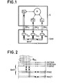
- a system S is represented schematically comprising several autonomous data processing units U, to Un. As has been recalled previously, these units can be of any kind. To fix the ideas, there will be described in the following a computer system S ′ comprising at least one data processor and peripheral units, without this being limiting the scope of the invention.
- a resource R which can be, for example, a data memory, to which one or more units U to Un of the system S wish to have access.
- the invention proposes a device for allocating DAR resources comprising interface circuits I A1 to I An and a multiple link channel BAR for coupling between the interface means of the bus type.
- the units U l to Un of the system S are coupled by a particular bus BAI to BAn, each with an interface circuit which is associated with it and which will be called in the following more briefly "interface”.
- these signals are of binary type and can therefore take two states: “Q” or "1" logic.
- each unit is assigned a number or address and a priority level. This assignment can be carried out by any procedure of the known art, preferably dynamically.
- the resource is allocated to a so-called winning unit at the end of a "race" between the units in competition during which this winning unit will have displayed the highest priority.
- the index i is an integer between 1 and n, n representing the number of units that can have access to a resource R of the system S.
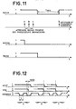
- FIG. 11 illustrates the case where three data processors a, b and c wish to acquire mastery of the same resource R.
- the start of the race is given by the descent of the signal "NCOUR" as indicated in the first line of the diagram in FIG. 11, caused simultaneously by the interfaces which first detected the triggering conditions. For each unit a new priority has been calculated before the falling edge "NCOUR". This priority is only displayed by the units (a, b, c) having positioned a request for the .resource. After the necessary duration of propagation of the signals, the unit having presented the highest priority is allocated the resource. This also has the effect of reducing the "PERSO” signal to the low level ("logic" 0) and also prohibiting any new race.
- each data processing unit One has its own basic work cycle.
- these cycle times are different from each other. These times are defined by an internal clock or by clock signals derived from a centralized clock.
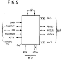
- FIG. 2 shows in more detail the bus BAR connecting the interface circuits IA1 to I An . It includes three bidirectional link wires carrying the "NCOUR, NDEMA and PERSO" signals.
- N the first letter in the acronyms identifying the signals used by the present invention means that these signals are active in the low state or "0" logic. Furthermore, these signals and their meanings are recalled in TABLE I placed at the end of this description.
- the bus "BAR” also comprises a channel with multiple bidirectional links “PRIO" conveying a binary word displaying the level of the highest priority calculated by the interfaces I A1 to I An .
- this channel may include eight connecting wires, each carrying a bit, the priority word being composed of a byte.
- the bus “BAR” furthermore comprises a channel, also with multiple bidirectional links "NACT", comprising for example four wires for carrying a binary word of four bits representing the number of the winning processor ("b" in the example chosen) or more generally of the winning unit U i .
- the early launch of "NCOUR" stems from the concern to take into account and satisfy as quickly as possible a resource request, that is to say in practice a request to launch a race, if the request is made early enough.
- the winning unit is the only applicant in the S system, it will only take one clock cycle to resume the resource after a period of inactivity.
- this system is a computer system comprising different units: peripheral units and / or processors, all connected to a data exchange channel of the bus type.
- this channel constitutes a particularly interesting example of a resource to be allocated, for which the units are in competition.
- Figures 3 and 4 schematically illustrate such a system.
- the system S comprises a link channel “BUS" for the exchange of data, this exchange being of the bidirectional type in the particular example described in relation to FIG. 3
- this channel can include, as illustrated in FIG. 4, a bus carrying address words "ADR”, for example thirty two bit words, a bus carrying data words "DON”, for example also thirty-two bit words divisible into bytes and a bus carrying "SPE" service signals. These generally include signals allowing secure exchanges such as validation and acknowledgment signals, as well as possibly clock and synchronization signals.
- This bus can also include ground links and links carrying the voltages necessary for the operation of the various units connected to it, depending on the nature of the technologies used.
- the precise architecture of the "BUS" link channel is outside the scope of the invention.
- Units U 1 to A system component can communicate with the "BUS" channel using specific buses “BUS 1 " to "BUS n " via interface circuits I D1 to I Dn .
- These circuits have the role of carrying out all the necessary adaptations making it possible to connect a particular unit U i to the "BUS" channel, adaptations as it is known of a technological or software nature. These aspects also go beyond the scope of the present invention. It may also be necessary to synchronize with respect to each other the interface circuits for the allocation of resources (I Ai ) and the data exchange interface circuits (I Di ). This synchronization is symboli sed by the links Sy 1 to S yn which can be multiple and include in particular clock signals.
- this peripheral unit or this processor takes control of the "BUS" channel, and can use this channel to exchange data with one or more other units, for example according to a procedure such as: addressing a particular unit followed by the exchange itself.
- the interface circuits (I Am ) for the allocation of the resources associated with each of the units in competition (Un) in a system S will now be described in more detail and an example of practical implementation will be given in the context of the approach which has just been recalled, that is to say when the resource to be allocated is a link channel for the exchange of data and the system S, a computer system.
- FIG. 5 schematically describes such an interface circuit. It is first of all assumed that each unit is provided with a clock, with a determined frequency delivering. clock signals H i . These circuits are in the form of a module I Ai which is interconnected between the bus "BAR" and the associated unit U i . It receives clock signals "2Hi" with a frequency twice that of the unit U i , these clock signals being synchronized with respect to each other. It is this clock which determines the minimum time of the run triggered by this interface IA i . The period must be greater than or equal to a minimum time to ensure proper functioning of the assembly, this time depending on the technology used.
- the interface I Ai is informed that the unit U i is requesting the channel "BUS" for exchanging data by the signal "DMB".
- the interface I Ai When the unit U i is elected, the interface I Ai returns the signal “ACTIVE” indicating that the channel "BUS" is available and that the data transfers can begin.
- a signal “NSYNMEM” makes it possible to synchronize the interface I Ai with the data exchange interface I Di also associated with the unit U i , as has been described in relation to FIGS. 3 and 4. This signal is one of the signals conveyed by the synchronization links (Sy i ) shown in this same figure.
- the signal “NSYNMEN” represented on the first line of the diagram of FIG. 12, active at low level or "0” logic according to the convention mentioned above, is a periodic signal of duration "T” at active level, duration equal to the time required to a data transfer on the "BUS" channel. It only interferes with the operation of the interface I Ai at the time of the last data transfer made.
- Part C of the diagram in FIG. 12 represents the case where a faulty operation has appeared: the "ACTIVE" signal fell before the last transfer to be made.
- a "TIMEOUT" signal sets the maximum time associated with the unit U i for mastering the "BUS" channel. This time is determined using a capacitor C for example, of a determined value acting on a monostable as will be described later. Any other method can be implemented, for example a purely numerical method using binary counters with modifiable capacity or associated with a logic for selecting a particular state.
- the unit In response to the "TIMEOUT" signal, the unit returns a "LIB” signal. releasing the interface.
- the interface receives on the "NSTA" channel a binary word representing the number assigned to the unit U i .
- the interface I A1 can be broken down into four separate blocks which interconnect to perform the allocation function as illustrated in FIG. 6.
- This part of the interface I Ai is a decision-making body for the actions to be carried out on the "BUS” channel and on the "BAR” bus. Display of the request to participate in a possible race, display of the activity on the "BUS” channel by the "PERSO” signal and control of the "TIMEOUT” signal.
- Logic gates performing the AND, OR, NON-AND and NON-OR logic functions will be used in the following in their usual acceptances and there is no need to describe them further. It will also be used inverters which aim to provide the logical complement of a binary signal present on their input.
- the high level is the logic "1”, represented in the context of the technology chosen by a voltage + 5V, the low level being the logic "0”, represented by a zero voltage.
- Type D flip-flops are also used, the configuration of which is useful to recall in more detail. This, as well as the truth table and the time diagram of such a flip-flop can be found among other publications, in the French book: "DE LA LOGIQUE CABLEE AUX MICROPROCESSEURS" by BERNARD et al., In volume 1 , chapter X.4, paes 136-138 (Editions EYROLLES; PARIS; 1979).
- Such a flip-flop comprises a data input D, a clock input H, a prepositioning input Pr ("preset”), a reset input CI ("clear”) and two outputs: true Q and inverted Q.
- Pr and CI inputs are asynchronous, and reset the flip-flop to "1" or "0” respectively, independently of the clock signals.
- Synchronous mode is defined by the data input D and the clock input H.
- the flip-flop copies the input D after the appearance of a rising edge of the clock signal applied to the input H, taking into account d '' a delay of taking into account, of the order of a few nanoseconds for the chosen technology.
- logic circuits whose outputs are connected in parallel on the lines constituting the "BAR" bus are of the so-called "open collector” type. Indeed the low level must be preponderant compared to the high level.
- the logic elements necessary for the production of the circuits can be chosen from the commercially available integrated circuits.
- the priority election function can be represented in symbolic form by a block receiving and emitting in particular the signal "NVAIN".
- This signal is internal to the IAi interface. It indicates that the requesting unit considers itself to have the highest priority after analysis of its priority by the signals carried on the "PRIO" bus (0 to 7).
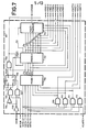
- block 60 receives "NSTA” signals (0 to 3) representing the number assigned to the unit U i and the signals "DMB” and "VCARTE” produced by the unit U i or the other blocks of the interface I Ai which will be described in the following.
- a unit U i To claim mastery of the "BUS" channel, a unit U i must participate in the race which ends with the determination of a winner. Participation is represented by the signal "PART”, is activated when a request from the unit U i is made when the race has not yet started: signal “NCOUR” at the high level. The unit's participation is activated during the entire occupation time of the "BUS" channel: "DMB” at the high level.
- circuits operate continuously. They include a PRIOR-1: 700 memory of the PROM type which fixes the priority according to the processor number (static number) given by the "NSTA" bus (NSTA-0 to NSTA-3) and the number of the last processor present on the "BUS" channel (active number) given by the "NACT" bus (NACT-0 to NACT-3).
- Memory 700 provides a four-bit code (a 0 - a 3 ) which. fixes the relative priority of the unit at an instant t. This priority is a function of the difference between "NACT" and "NSTA".
- the memory input circuits 700 corresponding to the bits of the "NACT" bus include inverters.
- the length of the binary words conveyed by the "NACT" and “NSTA” buses is given solely by way of non-limiting illustration of the invention.
- the "NSTA” number can be supplied by wired logic. It can indeed be permanently assigned to the unit U i . With four bits, sixteen units can be connected to the "BUS" channel.
- the content of the PRIOR-1: 700 memory is given by TABLE II placed at the end of this description.
- the output signals are identified by the symbols a 0 to a 3 .
- the table highlights the priority algorithm.
- the content of the memory may not be standard and thus respond to particular applications.
- the unit to which the number "NSTA” 0000 has been assigned fictitiously takes control of the channel "BUS” and transmits on the channel “NACT" the number "1111". It will then have the lowest priority when the "CUSTOM” signal is active (high level).
- the unit U i having the highest priority activates the signal "NVAIN” indicating that it has the highest priority.
- "NVAIN” evolves over time according to requests. It stabilizes during the race (interval T of the signal “NCOUR” in Figure 12).
- the signal “NVAIN” is produced by a multiplexer 702 receiving on its inputs the outputs of the memory “PRIOR-2”: 701 which correspond respectively to bits 0 to 6 of the binary word conveyed by the corresponding links of the bus "PRIO" (thus than to the respective outputs D 7 to D 1 of the memory 701.
- the addressing of this multiplexer to make the choice between the inputs is carried out in the example considered by a binary word of three bits constituted by the outputs a 0 to a 2 from the "PRIOR-1" memory: 700.
- the content of the memory “PRIOR-2”: 701 is given by way of example in TABLE III placed at the end of this description.
- the outputs D7 to D 1 respectively corresponding to the bits conveyed by the links “PRIOR-0" to "PRIOR-6".
- the output D 0 activates the multiplexer 702 (authorization input S).
- the addressing of the "PRIOR-2" memory: 701 is carried out using a five-bit word: a 0 , a l , a 2 , a 3 and "PRIO-7". This signal "PRIO-7".
- block 60 receives the signal "VCARTE” which allows it to display its number on the bus "NACT”. To do this, four NAND logic gates (709 to 712) are activated by the signal "VCARTE” so as to transmit the signals present on the links of the bus "NSTA" representing the number assigned to the unit U i .
- FIG. 8 describes a concrete embodiment of block 61. Its purpose is to develop the "PERSO”signals;"NDEMA” and “TIMEOUT” already described. To do this, it receives the other blocks of the interface I Ai or of the associated unit U. the following signals: "NCOUR”, “NVAINS” and its complement “NVAINS”, “ACTIVE”, “DMB” as well as clock signals "2H i 'with a frequency twice that of the clock signals of the unit U i , as previously mentioned.
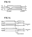
- a race is started if a unit is claimant and there is necessarily a winner.
- the "PERSO" signal is therefore disabled at the start of a race, as illustrated by the diagram in FIG. 14.
- the unit U i To obtain the "BUS” channel, the unit U i must activate the "NDEMA” line, especially if the "BUS" channel is occupied. This line is activated until the unit has been satisfied.
- the active unit must withdraw its request on the BAR bus so that requests from other units can be taken into account.
- block 61 receives a signal "NVAINS” which will be described later and a monostable 807 is triggered.
- the duration of the output signal is fixed by a capacitor C.
- the time “TIMEOUT” is signaled to the unit U i only if another unit has made a bus request ("NDEMA").
- the output signals which have just been described are produced using the OR logic gates: 801; NAND: 802, 804, 805; NOR: 806, of the inverter 803 and the rocker of type D: 800 and of the monostable 807 interconnected as indicated on figure 8.
- the marks "0” and “1” represent logical states “zero” and “a "permanent, that is to say according to the conventions accepted in the above, respectively of the low and high states.
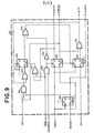
- FIG. 9 represents an example of a concrete embodiment of block 62 of FIG. 6. This block elaborates four sigrials: “NVAINS” and its complement “NVAINS”, “ACTIVE” and “VCARTE”.
- the activity of the unit U i is signaled by the signal "ACTIVE".
- the race must end with the election of a unit and the display of its number on the "NACT" bus.
- the D type flip-flop: 901 is reset to zero as soon as the race is finished: validation of the "NVAINS" signal.
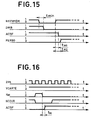
- the second case is that of early activation. This operating case is illustrated by the diagram in FIG. 16.
- the signal "VCARTE” in the high state indicates that the unit U i had last control of the "BUS" channel.
- the "NM” signal returns to the high state as soon as the "NCOUR” signal goes to the low state, thus indicating that the unit is master of the race.
- This signal is produced by block 63 which will be described later in connection with FIG. 10.
- the unit returns to the active state ("ACTIVE” signal in the high state), as soon as the first edge showing signals appears.
- the unit therefore returns to activity before the end of the race (" NCOUR " high).
- the third case is where the unit takes control of the "BUS" channel. while another unit had this control.
- the race function is used, the transition from mastery from one unit to another is carried out contiguously.
- This operating case is illustrated by the diagram in FIG. 17.
- control of the "BUS" channel. passes, for example, from a processor referenced “a” to a processor "b", at the end of a race caused by the fallout of the signal "NCOUR".
- the timing of the signals is clear from the diagram in Figure 17. It follows the procedures which have been described previously.
- the last block 63 is essentially intended to generate the race start signal "NCOUR” and incidentally the signal "NM”. To do this, it receives the signals "NDEMAN”, “ACTIVE”, “LIBR”, “DMB”, “PERSO” and “NSYNMEN” as well as the clock signals "ZH i ".
- a race is launched each time one or more units (U 1 to Un) wish to access the "BUS" channel and obtain control over it.
- the race makes it possible to "freeze” requests in order to elect the highest priority unit.
- the signals "LIB” and "DMB” are produced by the unit U i associated with a given interface I Ai .
- the race begins on the first edge of the clock signal "2H i " after the fall of the signal "DMB". It ends at the end of the last transfer if a clock period has already elapsed.
- the minimum duration of a race is therefore equal to one period of the clock.
- the signal "NCOUR” is produced using the signals transmitted to block 63 of FIG. 10 and which have been recalled in using D type flip-flops: 1001 to 1003, AND-NO logic gates: 1004, 1010, 1012 and. 1013; AND: 1005, 1006 and 1015; OR: 1008 and 1016; and inverters 1007, 1009, 1014, 1011 and 1017, interconnected as shown in Figure 10.
- the references “0" and “1” indicate two permanent states, low and high respectively.
- the "NCOUR” signal is only the complement of the copy of the "NM” signal. Otherwise, its duration (in the low state) is greater than that (high state) of the "NM” signal.
- the NON-ET.1013 logic gate is used to electrically decouple these two signals, the low state of the "NCOUR” signal on the corresponding link of the "BAR” bus being imposed by the interface producing a slower “NCOUR” signal.
Landscapes
- Engineering & Computer Science (AREA)
- Theoretical Computer Science (AREA)
- Physics & Mathematics (AREA)
- General Engineering & Computer Science (AREA)
- General Physics & Mathematics (AREA)
- Bus Control (AREA)
- Multi Processors (AREA)
Applications Claiming Priority (2)
| Application Number | Priority Date | Filing Date | Title |
|---|---|---|---|
| FR8107036A FR2503898B1 (fr) | 1981-04-08 | 1981-04-08 | Procede et dispositif d'allocation d'une ressource dans un systeme comportant des unites de traitement de donnees autonomes |
| FR8107036 | 1981-04-08 |
Publications (2)
| Publication Number | Publication Date |
|---|---|
| EP0063972A1 true EP0063972A1 (de) | 1982-11-03 |
| EP0063972B1 EP0063972B1 (de) | 1985-07-17 |
Family
ID=9257154
Family Applications (1)
| Application Number | Title | Priority Date | Filing Date |
|---|---|---|---|
| EP82400559A Expired EP0063972B1 (de) | 1981-04-08 | 1982-03-26 | Verfahren und Anordnung zur Hilfsquellenzuteilung in einem eine autonome Datenverarbeitungseinheit umfassenden System |
Country Status (6)
| Country | Link |
|---|---|
| US (1) | US4541043A (de) |
| EP (1) | EP0063972B1 (de) |
| JP (1) | JPS57176472A (de) |
| CA (1) | CA1180460A (de) |
| DE (1) | DE3264738D1 (de) |
| FR (1) | FR2503898B1 (de) |
Cited By (3)
| Publication number | Priority date | Publication date | Assignee | Title |
|---|---|---|---|---|
| EP0124806A1 (de) * | 1983-05-06 | 1984-11-14 | BBC Brown Boveri AG | Vergabeschaltung für Parallelbusse von Datenverarbeitungsanlagen |
| EP0137761A3 (de) * | 1983-09-27 | 1986-01-02 | Trw Inc. | Multi-Master-Busübertragungssystem mit paralleler Arbitrierung von Busanforderungen |
| EP0139563A3 (en) * | 1983-09-22 | 1986-09-17 | Digital Equipment Corporation | Control mechanism for multiprocessor system |
Families Citing this family (23)
| Publication number | Priority date | Publication date | Assignee | Title |
|---|---|---|---|---|
| GB2214334B (en) * | 1988-01-05 | 1992-05-06 | Texas Instruments Ltd | Integrated circuit |
| DE3472177D1 (en) * | 1983-07-19 | 1988-07-21 | Nec Corp | Apparatus for controlling a plurality of interruption processings |
| JPS6024647A (ja) * | 1983-07-20 | 1985-02-07 | Hitachi Ltd | システムの自律化資源管理方式 |
| US4763249A (en) * | 1983-09-22 | 1988-08-09 | Digital Equipment Corporation | Bus device for use in a computer system having a synchronous bus |
| US4787033A (en) * | 1983-09-22 | 1988-11-22 | Digital Equipment Corporation | Arbitration mechanism for assigning control of a communications path in a digital computer system |
| US4862350A (en) * | 1984-08-03 | 1989-08-29 | International Business Machines Corp. | Architecture for a distributive microprocessing system |
| US4789926A (en) * | 1985-08-06 | 1988-12-06 | International Business Machines Corporation | Digital data processing arbitration system |
| US4908749A (en) * | 1985-11-15 | 1990-03-13 | Data General Corporation | System for controlling access to computer bus having address phase and data phase by prolonging the generation of request signal |
| GB2196762B (en) * | 1986-10-27 | 1990-12-19 | Burr Brown Ltd | Interleaved access to global memory by high priority source |
| US4773037A (en) * | 1987-02-20 | 1988-09-20 | Gte Communication Systems Corporation | Increased bandwidth for multi-processor access of a common resource |
| JP2633900B2 (ja) * | 1988-04-22 | 1997-07-23 | 株式会社日立製作所 | 共通バス制御方法 |
| US5218702A (en) * | 1988-07-06 | 1993-06-08 | Motorola, Inc. | System for selecting request for a resource before decoding of requested resource address and validating selection thereafter |
| US5155854A (en) * | 1989-02-03 | 1992-10-13 | Digital Equipment Corporation | System for arbitrating communication requests using multi-pass control unit based on availability of system resources |
| US5253344A (en) * | 1991-09-05 | 1993-10-12 | International Business Machines Corp. | Method and apparatus for dynamically changing the configuration of a logically partitioned data processing system |
| US5265212A (en) * | 1992-04-01 | 1993-11-23 | Digital Equipment Corporation | Sharing of bus access among multiple state machines with minimal wait time and prioritization of like cycle types |
| JPH06337843A (ja) * | 1993-05-28 | 1994-12-06 | Fujitsu Ltd | データ転送制御方法 |
| US5729702A (en) * | 1993-06-21 | 1998-03-17 | Digital Equipment Corporation | Multi-level round robin arbitration system |
| JP2004513428A (ja) * | 2000-11-06 | 2004-04-30 | コーニンクレッカ フィリップス エレクトロニクス エヌ ヴィ | タスクへ資源配分を割当てる方法及びシステム |
| US7809874B2 (en) * | 2006-06-21 | 2010-10-05 | International Business Machines Corporation | Method for resource sharing in a multiple pipeline environment |
| US8727217B2 (en) | 2007-08-27 | 2014-05-20 | Texas Instruments Incorporated | Data detector for UHF RFID tags |
| US8314685B2 (en) * | 2007-08-27 | 2012-11-20 | Texas Instruments Incorporated | Data detector for UHF RFID tags |
| US7759171B2 (en) * | 2007-08-28 | 2010-07-20 | Spansion Llc | Method and structure of minimizing mold bleeding on a substrate surface of a semiconductor package |
| US11425752B2 (en) | 2016-10-19 | 2022-08-23 | Ipla Holdings Inc. | Radio interface protocol architecture aspects, quality of service (QOS), and logical channel prioritization for 5G new radio |
Citations (5)
| Publication number | Priority date | Publication date | Assignee | Title |
|---|---|---|---|---|
| GB1217355A (en) * | 1967-07-07 | 1970-12-31 | Ibm | Electronic service request system |
| US3553656A (en) * | 1969-06-03 | 1971-01-05 | Gen Electric | Selector for the dynamic assignment of priority on a periodic basis |
| FR2376464A1 (fr) * | 1976-12-30 | 1978-07-28 | Schlumberger Prospection | Procede et systeme de transmission de donnees sous forme numerique |
| US4177450A (en) * | 1975-12-31 | 1979-12-04 | Compagnie Internationale pour l'Informatique Cii - Honeywell Bull (Societe Anonyme) | Process and method to initiate a receiving and transmitting station linked by a connecting channel of an information exchange system consisting of several transmitting and receiving stations |
| US4209838A (en) * | 1976-12-20 | 1980-06-24 | Sperry Rand Corporation | Asynchronous bidirectional interface with priority bus monitoring among contending controllers and echo from a terminator |
Family Cites Families (5)
| Publication number | Priority date | Publication date | Assignee | Title |
|---|---|---|---|---|
| US4320502A (en) * | 1978-02-22 | 1982-03-16 | International Business Machines Corp. | Distributed priority resolution system |
| US4257095A (en) * | 1978-06-30 | 1981-03-17 | Intel Corporation | System bus arbitration, circuitry and methodology |
| US4281381A (en) * | 1979-05-14 | 1981-07-28 | Bell Telephone Laboratories, Incorporated | Distributed first-come first-served bus allocation apparatus |
| US4373183A (en) * | 1980-08-20 | 1983-02-08 | Ibm Corporation | Bus interface units sharing a common bus using distributed control for allocation of the bus |
| US4375639A (en) * | 1981-01-12 | 1983-03-01 | Harris Corporation | Synchronous bus arbiter |
-
1981
- 1981-04-08 FR FR8107036A patent/FR2503898B1/fr not_active Expired
-
1982
- 1982-03-26 EP EP82400559A patent/EP0063972B1/de not_active Expired
- 1982-03-26 DE DE8282400559T patent/DE3264738D1/de not_active Expired
- 1982-03-29 US US06/363,226 patent/US4541043A/en not_active Expired - Fee Related
- 1982-03-30 CA CA000399747A patent/CA1180460A/en not_active Expired
- 1982-04-08 JP JP57057409A patent/JPS57176472A/ja active Pending
Patent Citations (5)
| Publication number | Priority date | Publication date | Assignee | Title |
|---|---|---|---|---|
| GB1217355A (en) * | 1967-07-07 | 1970-12-31 | Ibm | Electronic service request system |
| US3553656A (en) * | 1969-06-03 | 1971-01-05 | Gen Electric | Selector for the dynamic assignment of priority on a periodic basis |
| US4177450A (en) * | 1975-12-31 | 1979-12-04 | Compagnie Internationale pour l'Informatique Cii - Honeywell Bull (Societe Anonyme) | Process and method to initiate a receiving and transmitting station linked by a connecting channel of an information exchange system consisting of several transmitting and receiving stations |
| US4209838A (en) * | 1976-12-20 | 1980-06-24 | Sperry Rand Corporation | Asynchronous bidirectional interface with priority bus monitoring among contending controllers and echo from a terminator |
| FR2376464A1 (fr) * | 1976-12-30 | 1978-07-28 | Schlumberger Prospection | Procede et systeme de transmission de donnees sous forme numerique |
Non-Patent Citations (3)
| Title |
|---|
| COMPUTER DESIGN, vol.17, no.1, avril 1978, Concord (US) * |
| IBM TECHNICAL DISCLOSURE BULLETIN, vol.22, no.3, août 1979, New York (US) * |
| IBM TECHNICAL DISCLOSURE BULLETIN, vol.23, no.7A, décembre 1980, New York (US) * |
Cited By (4)
| Publication number | Priority date | Publication date | Assignee | Title |
|---|---|---|---|---|
| EP0124806A1 (de) * | 1983-05-06 | 1984-11-14 | BBC Brown Boveri AG | Vergabeschaltung für Parallelbusse von Datenverarbeitungsanlagen |
| EP0139563A3 (en) * | 1983-09-22 | 1986-09-17 | Digital Equipment Corporation | Control mechanism for multiprocessor system |
| EP0137761A3 (de) * | 1983-09-27 | 1986-01-02 | Trw Inc. | Multi-Master-Busübertragungssystem mit paralleler Arbitrierung von Busanforderungen |
| US4626843A (en) * | 1983-09-27 | 1986-12-02 | Trw Inc. | Multi-master communication bus system with parallel bus request arbitration |
Also Published As
| Publication number | Publication date |
|---|---|
| FR2503898A1 (fr) | 1982-10-15 |
| US4541043A (en) | 1985-09-10 |
| DE3264738D1 (en) | 1985-08-22 |
| EP0063972B1 (de) | 1985-07-17 |
| FR2503898B1 (fr) | 1986-02-28 |
| CA1180460A (en) | 1985-01-02 |
| JPS57176472A (en) | 1982-10-29 |
Similar Documents
| Publication | Publication Date | Title |
|---|---|---|
| EP0063972B1 (de) | Verfahren und Anordnung zur Hilfsquellenzuteilung in einem eine autonome Datenverarbeitungseinheit umfassenden System | |
| EP0063071B1 (de) | Verfahren und Anordnung zur Übertragung numerischer Daten | |
| EP0167193B1 (de) | Arbitrierverfahren für Zugriffanforderungen von verschiedenen Pozessoren zu gemeinsamen Betriebsmitteln mittels eines gemeinsamen Buses | |
| EP0121030B1 (de) | Arbitervorrichtung für die Zuweisung eines gemeinsamen Betriebsmittels an eine ausgewählte Einheit eines Datenverarbeitungssystems | |
| FR2630839A1 (fr) | Procede et dispositif de controle de l'acces a un bus dans un systeme informatique | |
| FR2667706A1 (fr) | Antememoire hierarchique a circuits integres. | |
| FR2480460A1 (fr) | Dispositif pour transferer des informations entre des unites principales d'un systeme de traitement de donnees et un sous-systeme central | |
| FR2578071A1 (fr) | Installation de multitraitement a plusieurs processus | |
| EP0757465A1 (de) | HDLC-Anordnung mit verteiltem internen Bus | |
| FR2480458A1 (fr) | Dispositif pour transferer des informations entre des unites d'un systeme de traitement de donnees | |
| FR2519441A1 (fr) | Systeme de selection de priorite pour l'acces a un bus utilise en mode partage | |
| FR2487561A1 (fr) | Systeme de memoire dynamique | |
| FR2486290A1 (fr) | Dispositif de transmission rapide de donnees comportant un circuit de commande a acces direct a la memoire | |
| EP0077863A1 (de) | Abtasteinrichtung für Übertragungsleitungen, bestimmt für eine Übertragungssteuerung | |
| FR2549258A1 (fr) | Procede de commande pour transfert de donnees | |
| EP0039635B1 (de) | Zentralisiertes Zuteilungsverfahren und zentraler Arbiter | |
| FR2480459A1 (fr) | Systeme de traitement de donnees a un dispositif d'appariement d'adresses de memoire de controle | |
| FR2849228A1 (fr) | Dispositif de transfert de donnees entre deux sous-systemes asynchrones disposant d'une memoire tampon | |
| FR2595474A1 (fr) | Dispositif de controle et de verification du fonctionnement de blocs internes a un circuit integre | |
| EP0344052B1 (de) | Modularer Speicher | |
| FR2759178A1 (fr) | Circuit de gestion de memoire dans un environnement multi-utilisateurs avec requete et priorite d'acces | |
| EP0011540B1 (de) | Ein-/Ausgabe-Schnittstelle zwischen einem Datenvermittler und mehreren Übertragungsleitungen | |
| FR2717921A1 (fr) | Dispositif de gestion de conflit d'accès entre un CPU et des mémoires. | |
| FR2472245A1 (fr) | Operateur autonome de gestion de files d'attente ou de memoire | |
| EP0346420B1 (de) | Verfahren zum informationsaustausch in einem mehrprozessorsystem |
Legal Events
| Date | Code | Title | Description |
|---|---|---|---|
| PUAI | Public reference made under article 153(3) epc to a published international application that has entered the european phase |
Free format text: ORIGINAL CODE: 0009012 |
|
| AK | Designated contracting states |
Designated state(s): DE GB IT NL |
|
| 17P | Request for examination filed |
Effective date: 19821122 |
|
| ITF | It: translation for a ep patent filed | ||
| GRAA | (expected) grant |
Free format text: ORIGINAL CODE: 0009210 |
|
| AK | Designated contracting states |
Designated state(s): DE GB IT NL |
|
| REF | Corresponds to: |
Ref document number: 3264738 Country of ref document: DE Date of ref document: 19850822 |
|
| PGFP | Annual fee paid to national office [announced via postgrant information from national office to epo] |
Ref country code: NL Payment date: 19860331 Year of fee payment: 5 |
|
| PLBE | No opposition filed within time limit |
Free format text: ORIGINAL CODE: 0009261 |
|
| STAA | Information on the status of an ep patent application or granted ep patent |
Free format text: STATUS: NO OPPOSITION FILED WITHIN TIME LIMIT |
|
| 26N | No opposition filed | ||
| PG25 | Lapsed in a contracting state [announced via postgrant information from national office to epo] |
Ref country code: NL Effective date: 19871001 |
|
| NLV4 | Nl: lapsed or anulled due to non-payment of the annual fee | ||
| GBPC | Gb: european patent ceased through non-payment of renewal fee | ||
| PG25 | Lapsed in a contracting state [announced via postgrant information from national office to epo] |
Ref country code: DE Effective date: 19871201 |
|
| PG25 | Lapsed in a contracting state [announced via postgrant information from national office to epo] |
Ref country code: GB Effective date: 19881121 |