EP0064131A2 - Méthode numérique de modulation - Google Patents
Méthode numérique de modulation Download PDFInfo
- Publication number
- EP0064131A2 EP0064131A2 EP82101462A EP82101462A EP0064131A2 EP 0064131 A2 EP0064131 A2 EP 0064131A2 EP 82101462 A EP82101462 A EP 82101462A EP 82101462 A EP82101462 A EP 82101462A EP 0064131 A2 EP0064131 A2 EP 0064131A2
- Authority
- EP
- European Patent Office
- Prior art keywords
- phase
- signal
- vectors
- modulation
- assigned
- Prior art date
- Legal status (The legal status is an assumption and is not a legal conclusion. Google has not performed a legal analysis and makes no representation as to the accuracy of the status listed.)
- Granted
Links
Images

Classifications
-
- H—ELECTRICITY
- H04—ELECTRIC COMMUNICATION TECHNIQUE
- H04L—TRANSMISSION OF DIGITAL INFORMATION, e.g. TELEGRAPHIC COMMUNICATION
- H04L27/00—Modulated-carrier systems
- H04L27/32—Carrier systems characterised by combinations of two or more of the types covered by groups H04L27/02, H04L27/10, H04L27/18 or H04L27/26
- H04L27/34—Amplitude- and phase-modulated carrier systems, e.g. quadrature-amplitude modulated carrier systems
- H04L27/3405—Modifications of the signal space to increase the efficiency of transmission, e.g. reduction of the bit error rate, bandwidth, or average power
Definitions
- Such a digital modulation method is known from DE-PS 22 06 382.
- a method for modulating a carrier signal with higher-value digital signals, ie with those whose bit word length is greater than 2.
- the aim here is to modulate the carrier signal in such a way that it is as insensitive as possible to interference on the transmission link in order to be able to recover the original data signal from the modulated carrier signal without errors in the receiver.
- word lengths of the digital signal of 2 and maybe even 3 bits, it is sufficient to match the carrier signal with con modulate constant amplitude only in its phase. Limits are set to pure phase modulation very quickly, since as the number of possible bit words increases, the phase difference between the signals assigned to these bit words decreases.
- phase-amplitude modulation is carried out, ie the signals assigned to the possible bit words differ in phase and / or in amplitude.
- the choice of the phase and amplitude differences between the individual signals should now be made so that common disturbances occurring during signal transmission, such as noise, phase shifts, sloping amplitudes, multipath propagation and the like, do not disturb the signal amplitudes and phases so strongly that transitions between different ones Signal states occur.
- the document DE-PS 22 06 382 mentioned at the outset specifies a modulation method based on the phase amplitude modulation which has a greater signal-to-noise ratio than conventional methods (for example quadrature amplitude modulation QAM).
- QAM quadrature amplitude modulation
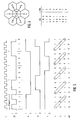
- the various signal states are created by the combination of two carrier signals controlled by the bit words and phase-shifted by 90 ° relative to one another and whose amplitude is weighted accordingly, three are at 120 ° relative to one another according to the method described in DE-PS 22 06 382 phase-shifted and amplitude-weighted carrier vibrations combined; namely, according to this method, the signal vectors are chosen with respect to their amplitude and phase so that their ends lie in the center points of regular hexagons of the same size, which are arranged in a honeycomb-like manner around the vector origin M in the phase plane (see FIG. 1).
- phase plane shown in Fig. 1 shows that the angles between some signal vectors, e.g. between vectors 1 and 11 or 5 and 15 etc. are quite small, which means that transitions between these vectors can easily occur due to phase shifts. With regard to phase shifts, this modulation method is therefore still quite susceptible to interference.
- the non-uniform angular division of the phase plane by the vectors is unfavorable for demodulation, since the demodulator must be able to precisely recognize several very different phase states. If, as here, the clear determination of the phase states is made more difficult, the probability of error in the demodulation increases.
- the invention is based on the object of specifying a digital modulation method of the type mentioned at the outset, as a result of which a modulation signal which is less susceptible to interference and more reliably demodulated can be generated compared to the prior art.
- the object is achieved in that only those are used as modulation signals whose vectors divide the 360 ° phase plane into equal-sized angular sections, and in addition a level-less zero signal is used as a modulation signal, which is obtained either by combining all three carrier oscillations with the same amplitude formed or realized by sending none of the three carrier vibrations.
- FIG. 2 shows a very simple vector system for a data signal with four 2-bit words; namely, according to the invention, a bit word is assigned signal 0, which has no level and of course no defined phase state, and signals are assigned to the remaining three bit words, the vectors 1, 2 and 3 of which have the same amplitudes and phase differences of 120 °.
- To the vectors are so-called interference circles are shown. They delimit the range in which an interference voltage vector can rotate around the tips of the signal vectors 0, 1, 2, 3 without a signal state being falsified by the interference voltage being superimposed. This means that in the event of a signal distortion.
- the demodulator then correctly recognizes the original signal state as long as the vector tip does not move out of the associated interference circuit. The further apart the interference circles are, the less likely it is that one signal state will be falsified into another.
- the zero signal is also used in the system in FIG. 2, which is generated by superimposing the three carrier oscillations of the same amplitude that are phase-shifted by 120 °, or is realized by emitting none of the three carrier oscillations, the other three signals can be very far in phase ( namely 120 ° apart, which results in an optimal signal-to-noise ratio between the signals.
- the signal vectors 1, 2 and 3 shown in FIG. 2 have the same length. It is also possible to form three differently long vectors from the combination of differently weighted carrier vibrations. This is useful in the extreme case of the 3-phase system, if the phase difference of 120 ° is not sufficient to clearly recognize the signal states in the receiver in the case of very strong phase disturbances.
- the stepped signal amplitudes then offer a further criterion for distinguishing the signals.
- FIG. 3 shows a vector system for a data signal with sixteen 4-bit words.
- the zero signal 0 is used.
- this Embodiment assigned only one bit word to the zero signal.
- the result is an ideal distribution of the signal vectors in the phase plane if, as in the known modulation method according to FIG. 1, each vector end in the middle. point of a regular hexagon.
- the other hexagons are clustered around a central hexagon, the center of which coincides with the vector of the zero signal, which is also the origin point 0 of vectors 1 to 15.
- This hexagon configuration means that the associated vectors divide the 360 ° phase plane into equal angular sections. Each vector therefore forms an angle of 30 ° with its two neighboring vectors. Modulation signals are obtained which can be demodulated with a very low probability of error due to optimally large and equidistant phase spacings; Should the amplitude spacing between the signals not be sufficient in the case of the densest hexagon arrangement shown in FIG. 3 in the case of very strong disturbances, the hexagons 8, 9, 10, 11, 12, 13, 14 and 15 of the outer hexagon ring can be further away from the origin point 0 become what an extension of the vectors ending in the centers of these hexagons.
- the hexagon system intended as a construction aid can, as the dotted hexagons in FIG. 3 indicate, be enlarged for further signal states.
- a pulse can be superimposed on a modulation signal of a defined phase at certain time intervals.
- this is the modulation signal 8.
- the associated vector is thus briefly extended, which is indicated by the broken line in FIG. 3.
- 4 shows the phase level with the vectors of the modulation signals 1 to 8 for digital signals with a 3-bit word length. 4 shows the assignment of the 8 possible bit words to the modulation signals 1 to 8. There are 6 vectors in the phase plane, namely those of the modulation signals 1 to 6, which each have a phase distance of 600 from their neighboring vectors. The remaining two bit words 000 and 111 are assigned to the zero signal. In order to be able to recognize during demodulation which of the two bit words has been assigned to a transmitted zero signal, additional information must be transmitted from which it can be derived whether bit word 000 or bit word 111 has been transmitted by the zero signal.
- the additional information provides two redundant bit words, which are also modulated and transmitted together with each modulated bit word of the data signal to be transmitted.
- T denotes the clock signal for the modulator.
- Any data signal DS to be modulated has been selected, its three-valued one Bit words 101, 011, 000, 001 and 110 are.
- the designations a, b and c stand for the three carrier oscillations which are phase-shifted by 120 ° relative to one another, and the combination of which can be used to generate the desired modulation signals. If a 1 is present at a, b or c, this means that the associated carrier oscillation is also used to form the modulation signal. If a 0 is present at a, b or c, the associated carrier oscillation is not involved in the resulting modulation signal.
- the data signal is fed to the modulator in series.
- the first bit of a word determines whether the carrier oscillation a (with phase 0 °), the second bit whether the carrier oscillation b (with phase 120 °), and the third bit whether the carrier oscillation c (with phase 240 °) contributes to the modulation.
- the digital signal DS is fed to the modulator in series, ie the values a, b and c are set in succession.
- the value table for a, b and c in the lower part of FIG. 5 illustrates this process (see framed bit values of a, b and c).
- the first bit of a word brings a to the value specified by the bit, the second bit sets b to it and finally the third bit sets c to the corresponding bit value.
- a, b and c At the end of a data signal word, a, b and c have the states 1 or 0 corresponding to the word, so that by combining the three carrier oscillations in accordance with the states of a, b and c, the modulation signal associated with the data signal word is produced.
- bit word 000 or bit word 111 in the modulator is transmitted to a zero signal has been assigned. If the previous redundant bit word was 000, 100, 010 or 001, the zero signal was based on bit word 000, because from these three redundant bit words only one word position can result from changing one bit position. In the same way, bit word 111 has certainly been assigned to the zero signal if the previous redundant bit word was 111, 011, 101 or 110. Instead of the previous redundant bit words, the subsequent redundant bit words can also be used to assess the zero signal. In addition, it is expedient to use the two redundant bit words for error detection in all other transmitted data signals. Under certain circumstances, error correction is also possible using the redundant bit words.
- the three modulation signals are to be coordinated in a very specific way. Namely, the three modulation signals are transmitted with a 120 ° phase shift with respect to their envelope. Only the sine or cosine fundamental wave, which is obtained by suppressing all harmonics of the otherwise rectangular envelope, serves as the envelope of each modulation signal. According to this method, advantageously no greater bandwidth of the transmission channel is required than for the transmission of a modulation signal with a rectangular envelope, the width of which corresponds to the period for the serial delivery of a data signal word to the modulator.
- bit words can of course also be transferred to digital signals with higher-order bit words, for example four different bit words can already be assigned to the zero signal for 2 4 : 16 bit words. It should only be bit words that differ from one another in at least three bit positions.
Landscapes
- Engineering & Computer Science (AREA)
- Computer Networks & Wireless Communication (AREA)
- Signal Processing (AREA)
- Digital Transmission Methods That Use Modulated Carrier Waves (AREA)
- Oscillators With Electromechanical Resonators (AREA)
- Holo Graphy (AREA)
- Liquid Crystal (AREA)
Priority Applications (1)
| Application Number | Priority Date | Filing Date | Title |
|---|---|---|---|
| AT82101462T ATE12998T1 (de) | 1981-04-30 | 1982-02-26 | Digitales modulationsverfahren. |
Applications Claiming Priority (2)
| Application Number | Priority Date | Filing Date | Title |
|---|---|---|---|
| DE3117134 | 1981-04-30 | ||
| DE19813117134 DE3117134A1 (de) | 1981-04-30 | 1981-04-30 | Digitale modulationsverfahren |
Publications (3)
| Publication Number | Publication Date |
|---|---|
| EP0064131A2 true EP0064131A2 (fr) | 1982-11-10 |
| EP0064131A3 EP0064131A3 (en) | 1983-03-16 |
| EP0064131B1 EP0064131B1 (fr) | 1985-04-24 |
Family
ID=6131161
Family Applications (1)
| Application Number | Title | Priority Date | Filing Date |
|---|---|---|---|
| EP82101462A Expired EP0064131B1 (fr) | 1981-04-30 | 1982-02-26 | Méthode numérique de modulation |
Country Status (7)
| Country | Link |
|---|---|
| US (1) | US4495477A (fr) |
| EP (1) | EP0064131B1 (fr) |
| AT (1) | ATE12998T1 (fr) |
| CA (1) | CA1188759A (fr) |
| DE (2) | DE3117134A1 (fr) |
| DK (1) | DK159707C (fr) |
| IE (1) | IE53013B1 (fr) |
Families Citing this family (11)
| Publication number | Priority date | Publication date | Assignee | Title |
|---|---|---|---|---|
| US4538284A (en) * | 1981-03-25 | 1985-08-27 | Ese Limited | Signal structures with data encoding/decoding for QCM modulations |
| GB2118003B (en) * | 1982-02-02 | 1985-07-31 | Racal Milgo Ltd | Differential encoder and decoder for transmitting binary data |
| JPS59165540A (ja) * | 1983-03-09 | 1984-09-18 | Ricoh Co Ltd | デ−タ伝送制御方式 |
| US4894844A (en) * | 1987-06-12 | 1990-01-16 | Codex Corporation | Signal constellations |
| US4959842A (en) * | 1988-04-13 | 1990-09-25 | Codex Corporation | Signal constellations |
| DE3934187C1 (fr) * | 1989-10-13 | 1991-03-14 | Ant Nachrichtentechnik Gmbh, 7150 Backnang, De | |
| US6009132A (en) * | 1997-07-25 | 1999-12-28 | Globespan Semiconductor, Inc. | System and method for obtaining clock recovery from a received data signal |
| GB9807403D0 (en) * | 1998-04-06 | 1998-06-03 | Northern Telecom Ltd | Apparatus and method for reducing cross-talk in broadband systems and method of improving data recovery |
| JP7110386B2 (ja) | 2018-04-12 | 2022-08-01 | レイセオン カンパニー | 光信号における位相変化検出 |
| US10554306B1 (en) | 2019-03-13 | 2020-02-04 | Raytheon Company | Constant envelope path-dependent phase modulation |
| US11411654B1 (en) | 2021-03-24 | 2022-08-09 | Raytheon Company | Method for generating a constant envelope waveform when encoding multiple sub channels on the same carrier |
Family Cites Families (6)
| Publication number | Priority date | Publication date | Assignee | Title |
|---|---|---|---|---|
| JPS5038488B1 (fr) * | 1970-08-14 | 1975-12-10 | ||
| JPS5125303B1 (fr) * | 1971-02-10 | 1976-07-30 | ||
| US3845412A (en) * | 1973-10-12 | 1974-10-29 | Microwave Ass Inc | Digital modulate/demodulate system |
| US3983485A (en) * | 1975-02-28 | 1976-09-28 | Rixon Inc. | Multi-phase and multi-amplitude level modulator and modulation and demodulation methods |
| DE2550795A1 (de) * | 1975-11-10 | 1977-05-26 | Hycom Inc | Datenuebertragungssystem mit einem optimalen acht-vektoren signalisier- schema |
| US4404532A (en) * | 1978-09-29 | 1983-09-13 | Communications Satellite Corporation | Modulator having improved bandwidth and power requirements |
-
1981
- 1981-04-30 DE DE19813117134 patent/DE3117134A1/de not_active Withdrawn
-
1982
- 1982-02-26 DE DE8282101462T patent/DE3263226D1/de not_active Expired
- 1982-02-26 AT AT82101462T patent/ATE12998T1/de active
- 1982-02-26 EP EP82101462A patent/EP0064131B1/fr not_active Expired
- 1982-04-27 US US06/372,386 patent/US4495477A/en not_active Expired - Fee Related
- 1982-04-29 DK DK192282A patent/DK159707C/da not_active IP Right Cessation
- 1982-04-29 IE IE1012/82A patent/IE53013B1/en not_active IP Right Cessation
- 1982-04-29 CA CA000401958A patent/CA1188759A/fr not_active Expired
Also Published As
| Publication number | Publication date |
|---|---|
| ATE12998T1 (de) | 1985-05-15 |
| DE3117134A1 (de) | 1982-11-18 |
| IE53013B1 (en) | 1988-05-11 |
| DK159707B (da) | 1990-11-19 |
| US4495477A (en) | 1985-01-22 |
| EP0064131A3 (en) | 1983-03-16 |
| DE3263226D1 (en) | 1985-05-30 |
| DK159707C (da) | 1991-04-15 |
| CA1188759A (fr) | 1985-06-11 |
| EP0064131B1 (fr) | 1985-04-24 |
| DK192282A (da) | 1982-10-31 |
| IE821012L (en) | 1982-10-30 |
Similar Documents
| Publication | Publication Date | Title |
|---|---|---|
| DE3883194T2 (de) | Dekodierverfahren und Vorrichtung mit Auslöschungsdetektion für Mehrpegelübertragungssysteme. | |
| DE3886828T2 (de) | Doppelpolarisationsübertragungssystem. | |
| DE69131503T2 (de) | Radio für verschiedene modulationsarten | |
| DE2245189B2 (de) | Vorrichtung zur Übertragung eines restseitenbandträgermodulierten Mehrpegelsignals und eines Synchronisier-Pilotsignals | |
| EP0064131B1 (fr) | Méthode numérique de modulation | |
| DE2625038B2 (de) | Konverter zur Konvertierung einer Folge digitaler binarer Signale in eine Folge mehrphasig phasenmodulierter Tragerimpulse bzw. umgekehrt | |
| DE19530114C2 (de) | Modulator und Verfahren zur IQ-Modulation | |
| EP0249045B1 (fr) | Procédé d'obtention d'un signal de différence de phase | |
| DE2817836C3 (de) | Verfahren zur Mehrfachübertragung digitaler Signale sowie Einrichtung zur Durchführung eines solchen Verfahrens | |
| EP0281652A1 (fr) | Procédé d'obtention d'un signal de différence de phase | |
| DE2452997A1 (de) | Verfahren und anordnung zur funkuebertragung von binaeren informationssignalen | |
| DE2354718B2 (de) | Demodulationsverfahren für phasenumgetastete Schwingungen und Schaltungsanordnung zur Durchführung des Verfahrens | |
| DE69206199T2 (de) | Verfahren zur Kompensierung der Abhängigkeit des nützlichen Sendersignals von der Übertragungsfunktion eines Kombinierer-Filters. | |
| DE60128294T2 (de) | Signalisierung der Modulationsart in adaptiven Modulationssystemen | |
| EP0011749B1 (fr) | Circuit de correction de données | |
| DE2544124C3 (de) | Rückkopplungsentzerrer | |
| WO2001060005A1 (fr) | Procede de determination de la puissance des porteurs restante pour un signal multiporteur a modulation d'amplitude en quadrature, en mode 8k, selon la norme dvb-t | |
| DE2300762B2 (de) | Anordnung zur Wiedergewinnung der Information einer kodierten Nachricht | |
| DE2020805C3 (de) | Entzerrer zur Entzerrung von phasen- oder quadraturmodulierten Datensignalen | |
| EP0080020A1 (fr) | Procédé pour la détermination des instants d'échantillonnage d'un signal reçu en modulation de quadrature de phase manipulée ou en modulation de quadrature d'amplitude | |
| DE69211535T2 (de) | Sender und empfänger für phasenmodulation | |
| DE3429959C2 (de) | Verfahren zur Nachrichtenübertragung mittels Frequenzumtast-Modulation | |
| DE1591054B2 (de) | Nachrichtenempfaenger fuer frequenzmodulierte signale | |
| DE2915067C2 (de) | Verfahren zur Redundanzreduktion bei der Übertragung digital codierter Analogsignale | |
| DE3010537A1 (de) | Anordnung zur uebertragung digitaler daten |
Legal Events
| Date | Code | Title | Description |
|---|---|---|---|
| PUAI | Public reference made under article 153(3) epc to a published international application that has entered the european phase |
Free format text: ORIGINAL CODE: 0009012 |
|
| AK | Designated contracting states |
Designated state(s): AT BE CH DE FR GB IT LI LU NL |
|
| PUAL | Search report despatched |
Free format text: ORIGINAL CODE: 0009013 |
|
| AK | Designated contracting states |
Designated state(s): AT BE CH DE FR GB IT LI LU NL |
|
| RAP1 | Party data changed (applicant data changed or rights of an application transferred) |
Owner name: AEG - TELEFUNKEN NACHRICHTENTECHNIK GMBH |
|
| RAP1 | Party data changed (applicant data changed or rights of an application transferred) |
Owner name: ANT NACHRICHTENTECHNIK GMBH |
|
| 17P | Request for examination filed |
Effective date: 19830712 |
|
| ITF | It: translation for a ep patent filed | ||
| GRAA | (expected) grant |
Free format text: ORIGINAL CODE: 0009210 |
|
| AK | Designated contracting states |
Designated state(s): AT BE CH DE FR GB IT LI LU NL |
|
| REF | Corresponds to: |
Ref document number: 12998 Country of ref document: AT Date of ref document: 19850515 Kind code of ref document: T |
|
| REF | Corresponds to: |
Ref document number: 3263226 Country of ref document: DE Date of ref document: 19850530 |
|
| ET | Fr: translation filed | ||
| PLBE | No opposition filed within time limit |
Free format text: ORIGINAL CODE: 0009261 |
|
| STAA | Information on the status of an ep patent application or granted ep patent |
Free format text: STATUS: NO OPPOSITION FILED WITHIN TIME LIMIT |
|
| 26N | No opposition filed | ||
| ITTA | It: last paid annual fee | ||
| PGFP | Annual fee paid to national office [announced via postgrant information from national office to epo] |
Ref country code: GB Payment date: 19920210 Year of fee payment: 11 |
|
| PGFP | Annual fee paid to national office [announced via postgrant information from national office to epo] |
Ref country code: FR Payment date: 19920214 Year of fee payment: 11 |
|
| PGFP | Annual fee paid to national office [announced via postgrant information from national office to epo] |
Ref country code: LU Payment date: 19920225 Year of fee payment: 11 |
|
| PGFP | Annual fee paid to national office [announced via postgrant information from national office to epo] |
Ref country code: BE Payment date: 19920226 Year of fee payment: 11 |
|
| PGFP | Annual fee paid to national office [announced via postgrant information from national office to epo] |
Ref country code: NL Payment date: 19920229 Year of fee payment: 11 |
|
| PGFP | Annual fee paid to national office [announced via postgrant information from national office to epo] |
Ref country code: CH Payment date: 19920323 Year of fee payment: 11 |
|
| EPTA | Lu: last paid annual fee | ||
| PG25 | Lapsed in a contracting state [announced via postgrant information from national office to epo] |
Ref country code: LU Free format text: LAPSE BECAUSE OF NON-PAYMENT OF DUE FEES Effective date: 19930226 Ref country code: GB Effective date: 19930226 |
|
| PG25 | Lapsed in a contracting state [announced via postgrant information from national office to epo] |
Ref country code: LI Effective date: 19930228 Ref country code: CH Effective date: 19930228 Ref country code: BE Effective date: 19930228 |
|
| PGFP | Annual fee paid to national office [announced via postgrant information from national office to epo] |
Ref country code: DE Payment date: 19930421 Year of fee payment: 12 |
|
| BERE | Be: lapsed |
Owner name: ANT NACHRICHTENTECHNIK G.M.B.H. Effective date: 19930228 |
|
| PG25 | Lapsed in a contracting state [announced via postgrant information from national office to epo] |
Ref country code: NL Effective date: 19930901 |
|
| NLV4 | Nl: lapsed or anulled due to non-payment of the annual fee | ||
| GBPC | Gb: european patent ceased through non-payment of renewal fee |
Effective date: 19930226 |
|
| PG25 | Lapsed in a contracting state [announced via postgrant information from national office to epo] |
Ref country code: FR Effective date: 19931029 |
|
| REG | Reference to a national code |
Ref country code: CH Ref legal event code: PL |
|
| REG | Reference to a national code |
Ref country code: FR Ref legal event code: ST |
|
| PGFP | Annual fee paid to national office [announced via postgrant information from national office to epo] |
Ref country code: AT Payment date: 19940323 Year of fee payment: 13 |
|
| PG25 | Lapsed in a contracting state [announced via postgrant information from national office to epo] |
Ref country code: DE Effective date: 19941101 |
|
| PG25 | Lapsed in a contracting state [announced via postgrant information from national office to epo] |
Ref country code: AT Effective date: 19950226 |