EP0064431A1 - Vorrichtung zur Korrektur nichtlinearer Videofrequenz mit selektiver Zweckmässigkeit - Google Patents
Vorrichtung zur Korrektur nichtlinearer Videofrequenz mit selektiver Zweckmässigkeit Download PDFInfo
- Publication number
- EP0064431A1 EP0064431A1 EP82400614A EP82400614A EP0064431A1 EP 0064431 A1 EP0064431 A1 EP 0064431A1 EP 82400614 A EP82400614 A EP 82400614A EP 82400614 A EP82400614 A EP 82400614A EP 0064431 A1 EP0064431 A1 EP 0064431A1
- Authority
- EP
- European Patent Office
- Prior art keywords
- output
- correction
- signal
- channel
- input
- Prior art date
- Legal status (The legal status is an assumption and is not a legal conclusion. Google has not performed a legal analysis and makes no representation as to the accuracy of the status listed.)
- Granted
Links
Images


Classifications
-
- H—ELECTRICITY
- H04—ELECTRIC COMMUNICATION TECHNIQUE
- H04N—PICTORIAL COMMUNICATION, e.g. TELEVISION
- H04N5/00—Details of television systems
- H04N5/38—Transmitter circuitry for the transmission of television signals according to analogue transmission standards
Definitions
- the invention relates to the correction of amplitude non-linearity in a television transmitter, and more particularly to a video frequency non-linearity correction device with selective efficiency.
- the aim of the amplitude correction device according to the invention is to correct the low frequency non-linearities introduced into the power stages of a television transmitter.
- the principle of such a correction is to introduce on the video frequency signal before intermediate frequency modulation, a predistortion, in the lower part of the video frequency spectrum, complementary to that which is generated in the high frequency power stages.
- a threshold corrector circuit which establish the amplitude-amplitude characteristic opposite to that of the output stage by means of a threshold corrector circuit, the correction being effected by means of six to eight adjustment parameters so that the definition of the precorrection characteristic is sufficient: three to four action thresholds are for example fixed, associated with three or four slopes corresponding to the effectiveness of the correction introduced at the threshold point.
- This precorrector circuit is inserted before intermediate frequency modulation in the video signal processing chain, at a point where the amplitude of this signal is well defined, that is to say after alignment and automatic gain control.
- correction circuits can be provided in a television system to pre-correct the distortions so that the signal from the high frequency stages has a suitable linearity.
- These systems can for example be threshold precorrectors acting at intermediate frequency (used in particular when the video frequency signal is not available, for example in television repeaters), differential gain correctors using a third-order non-linearity generator, or premodulation correction circuits.
- a correction device of the type using a third-order non-linearity generator only allows progressive amplitude correction: expansion from white to black for negative modulation or expansion from black to white for positive modulation .
- an amplitude modulation transmission system for the transmission of the television picture signal, carries out the amplification by means of a two-channel device parallel, one for the amplification of a reduced carrier signal with a polarized class AB amplifier, and the other for the amplification of a pure carrier signal with a class C amplifier, the signals obtained being combined for obtain the amplified signal to be transmitted.
- the class AB amplifier introduces distortion for low levels due to the non-linearity of its transfer characteristic, its gain being stronger for low levels.
- the subject of the invention is a correction device which makes it possible to solve the problem of the expansion of the intermediate levels in a television transmitter, by means of a frequency selective, easy-to-adjust video frequency correcting circuit which moreover allows do not affect the differential gain.
- This correction circuit can be adapted to pre-correct any amplitude distortion, which would affect the video frequency signal at the output of the high frequency stages in the absence of such a circuit, whatever the type of modulation used in the transmitter.
- a device for correcting video non-linearity with selective efficiency, for the pre-correction of non-linearities introduced on the video signal in the high frequency stages of a television equipment comprises an input video signal signal connected to the input of a distributor having at least two outputs respectively connected to the input of a broadband channel and to the input of a low frequency correction channel, this correction channel comprising a low-pass filter, the output of which is coupled to at least one threshold corrector circuit comprising means for selecting the ranges of levels to be corrected and associated amplitude adjustment means, the output of the corrector circuit being coupled to the output of the low frequency correction channel, the outputs of the broadband channel and the correction channel being connected to two corresponding inputs of an output circuit combining the signals corresponding output signals to form a pre-corrected signal affected by non-linearities complementary to those to be corrected.
- Figure la represents a test luminance signal, Vg F , applied to the video input of the transmitter.
- This signal comprises a synchronization pulse between 0 and 0.3 Volt and an increasing signal in the form of stair steps up to 1 volt.
- Figure 1b shows a modulated signal with reduced carrier (V HF ) m . Its amplification by a class AB amplifier, associated with an amplification of the carrier not modulated by a class C amplifier, makes it possible to very significantly increase the efficiency.
- the low modulation levels undergo an expansion; these low levels correspond to the average gray of the video frequency luminance signal.
- Figure lc shows this differentiated demodulated signal (V BF ) d , to show the differences in levels.
- This gray non-linearity can be of the order of 10%.
- FIG. 3 represents the block diagram of the correction device inserted in the video frequency stages of television equipment, according to the invention.
- This device comprises a video frequency signal input E 1 connected to the input of a distributor 1, this input being supplied by the output signal of a synchronization separator circuit not shown which only transmits the video signal, excluding synchronization pulses.
- This signal is therefore distributed by the distributor 1 in two channels.
- a so-called direct, broadband channel mainly comprises a delay line 2, and a channel, called processing channel, comprising in series a low-pass filter 3 intersecting the frequency spectrum at 2.4 MHz for example, that is to say the signal transmitted in double band.
- This low-pass filter 3 has its output connected to the input of an inverting amplifier 4, the output of which is connected to the input of a separator circuit 5.
- This separator circuit also includes a second input connected to the output d an alignment circuit 6 receiving pulses intervening during the intervals of synchronization signals; this alignment makes it possible to fix the level of suppression in the separator circuit 5.
- the delay introduced by the delay line 2 of the broadband channel is equal to the delay introduced into the d processing auxiliary channel, this delay being mainly due to the low-pass filter 3.
- the processing path further comprises a correcting circuit particularly suitable for correcting the expansion of the medium grays; this corrector circuit 7 is inserted between an output of the separator 5 and an input of an output summator 8, the first input of which is connected to the output of the delay line of the broadband channel.
- This corrector circuit 7 makes it possible to select, by a diode system, a part of the low-frequency video signal.
- This selected signal which has a reverse polarity to that of the corresponding part of the signal in the broadband channel due to the inverting amplifier 4, is added to the broadband signal transmitted by the main channel in the adder 8.
- this correction device makes it possible to combine, with the video frequency non-linearity pre-correction function, the function of limiting the signal to video frequency, such a limitation being necessary so that the modulation rate is not too great.
- the separator circuit 5 has a second output connected to the input of a clipping circuit 9 selecting the part of the signal which must be clipped.
- the output of this clipping circuit is connected to a third input of the output summing circuit 8. If the limitation threshold for high amplitudes is fixed for example at 0.5 volts, when the signal at the video input does not exceed 0 , 5 volts, no signal appears at the output of the clipper 9 and the video signal is transmitted as is at the output of the summator 8 by the broadband channel.
- the output signal from the clipper is added to the video signal from the broadband channel to provide the video frequency signal limited to the output of the adder 8 to the modulator.
- the amplitude conditions achieved in the summator 8 allow to have a zero slope after the limitation threshold.
- This circuit for limiting the high amplitudes makes it possible, because it only processes low frequency components of the spectrum, to respect the amplitude and the phase of the signal carrying the chrominance information even for the levels which must be limited; it also makes it possible to respect the bandwidth of this chrominance signal and not to introduce any disturbance if the input signal does not exceed the nominal amplitude of 0.5 volts for example.
- the action threshold of the limiter is very straightforward because the conduction characteristic of the clipping diode in the auxiliary processing channel is brutal.
- FIG. 4 represents the shape of the signals at different points of the device represented in FIG. 3 when the correction rate by the corrector circuit 7 is zero: the signal E 1 at the input of the distributor 1, assumed to be a ramp for the signal the luminance on which the chrominance subcarrier is superimposed; the signal E4 at the input of the inverting amplifier 4, this signal no longer comprising the chrominance subcarrier due to the low-pass filtering; the signal S 4 at the output of the amplifier 4; the signal S 9 at the output of the clipper; and the signal S 8 at the output of the adder 8.
- the signal S 8 is limited for high amplitudes of the video signal, that is to say white.
- FIG. 5 represents a detailed embodiment of the corrector circuit 7.
- the input E 7 is connected via an input resistor R 1 to the point common to two diodes D 1 and D 2 , the first being mounted in the direct direction and the second in the opposite direction, the others terminals of these two diodes being connected to the cursors of two potentiometers, respectively P and P 2 .
- These two potentiometers are connected on the one hand to ground, on the other hand to the first terminals of two resistors, respectively R 2 and R 3 , the other terminals of which are connected to a point of positive potential, + V 1 .
- the terminal common to the two diodes D 1 and D 2 and to the resistor R 1 is also connected to a terminal of a potentiometer P 3 , the other terminal of which is connected to ground.
- the cursor of this potentiometer P 3 is connected to the base of a pnp type transistor T whose collector is connected to the positive supply terminal, + V 1 and whose emitter is connected to the negative supply terminal -V 2 via a network of resistors R 4 , R 5 .
- the point common to these two resistors is connected by an output resistor R 6 to the output terminal of the correcting circuit S 7 .
- This circuit operates as follows: the part of the signal above a threshold S 2 is clipped by the diode D 2 and the part below a threshold S 1 is clipped by the diode D 1 .
- the clipping thresholds, S 1 and S 2 are adjusted by potentiometers P 1 and P 2 whose sliders behave like voltage sources.
- a part of the correction signal is taken from the cursor of the potentiometer P 3 and transmitted to the common collector circuit formed by the transistor T and the resistors R 4 and R 5 .
- the summation of the correction signal thus obtained to the signal of the broadband channel available at the output of the delay line is done by the resistors R 4 , R 5 and R 6 and the equivalent impedance of the circuit seen through the line at delay, in parallel with the impedance of the summator.
- the adjustment of the correction efficiency by the potentiometer P 3 causes a variation in the amplitude of the output signal, S 8 .
- This variation is caught up in another stage of the transmitter, preferably downstream of the correction device so as not to modify the setting of the correction thresholds and of the white limitation threshold.
- the modulation depth keeps a suitable value.
- This circuit therefore makes it possible to determine the range of the levels of the video frequency signal between the two thresholds s 1 and s 2 in which the correction will be effective.
- the effectiveness of the correction determined by the potentiometer P 3 is not limited. It can be adapted to the type of faults to be corrected.
- the defect is corrected by subjecting the video signal to compression in medium gray. Given the rate of non-linearity in the signal, an efficiency of 20% maximum for the correction is very sufficient to correct the defect described above.
- FIG. 7 represents an embodiment of such a correction circuit in which three correction zones are determined, the effectiveness of the correction in each of these zones being able to be adjusted independently of the efficiencies fixed in the other zones; the system further comprises reversing means making it possible to carry out either a compression or an expansion for each of these zones.
- the input E 7 of the correction circuit 7 is connected by three input resistors R a , R b and R c to limitation diodes D 1a , D 2b and D 1b , D 2c .
- the second terminals of these diodes are connected to voltage sources U 1 , U 2 , U 3 and U 4 determined by resistors R 7 , R 8 , R 9 , R 10 and R 11 connected in series between the source of positive supply + V 1 and ground.
- the diode D 1a clips the values of the video signal below the threshold U 1
- the diode D 2c clips the values above the voltage U 4
- the diodes D 1b and D 2b clip the values respectively below the threshold U 3 and above the threshold U2.
- the clipped signals available on the second terminals of the resistors R, R b and R c are transmitted to separating transistors respectively T 1 , T 2 and T 3 via potentiometers for adjusting the efficiency, respectively P 4 , P 5 P 6 .
- the transistors T 1 , T 2 and T 3 are mounted as a common collector, their collector being connected to the positive supply terminal + V 1 and their emitters being connected to the negative supply terminal -V 2 by polarization resistors respectively R 12 , R 13 and R 14 '
- the signals of correction available on the emitters of the transistors T 1 , T 2 and T 3 are transmitted to the output terminals S 7 and S ' 7 respectively via the double switches I 1 , I 2 and I 3 .
- These output terminals S 7 and S ' 7 are intended to be connected at different points on the device; the terminal S 7 is connected as previously to an input of the adder 8, the result being a compression of the video signal in the corresponding zones; terminal S ' 7 is connected to an input of a subtractor 10 shown in dotted lines in FIG. 3, the result being an expansion of the video signal in the corresponding zones.
- the potentiometers P 4 , P 5 and P6 make it possible to measure the amplitude of the correction signal combined with the video signal, and therefore the effectiveness of this correction.
- the switches I 1 , 1 2 and 1 3 having their movable part to ground switch to ground the resistors which do not transmit the correction signal so that there is no disturbance in the device.
- Such a circuit allows very simple compression or expansion with adjustable efficiency in predetermined areas; the adjustment of the efficiency in each action zone does not modify this action zone itself and the adjustment of efficiency being independent of each other.
- FIGS. 8a, 8b and 8c show examples of precorrected signals (after differentiation) capable of being obtained at the output of the correction device for given settings and determined positions of the double switches.
- FIG. 8a shows an expansion in black (first steps of the signal) and a compression in white (last steps of the signal), the intermediate levels not being modified, V N being the nominal level.
- Figure 8b shows black expansion, gray compression and white expansion.
- the positions of the double inverters I 1 , 1 2 and I 3 in FIG. 7 correspond to this type of correction.
- Figure 8c shows black, gray and white compression.
- the improvement consisting in providing two outputs which do not bring any disturbance makes it possible to easily choose by the inverters the sign of the correction applied in a determined zone.
- Such a circuit like the first embodiment described with reference to FIG. 3, does not disturb either the differential gain or the differential phase because it acts only on the filtered signal at video frequency and not the signals of frequencies higher than the cut-off frequency of the low-pass filter, for example 2.4 MHz.
- the embodiment of the correction circuit described with reference to FIG. 7 is provided with three "correction cells". It is possible to increase the number of such correction cells to adapt the correction characteristic to the fineness of the desired correction; in practice, a six or seven cell system makes it possible to obtain a very precise correction characteristic.
- a low frequency channel has been represented, the output signal of this correction channel being combined with the output signal of the broadband channel to carry out selective pre-correction in the low frequency band of the video signal.
- an analog device to pre-correct the video frequency signal selectively in another frequency band, for example to correct a linearity defect appearing only in the band of the timing subcarrier.
- the corresponding parts of the signal are selected by a bandpass filter; the range of levels to be corrected is selected as above by thresholds from the low frequency signal and the effectiveness of the correction is adjusted by varying the amplitude of this signal.
- This signal makes it possible to model the amplitude of the signal selected in the band, these two signals being applied to the inputs of a modulator whose output signal is combined with the unprocessed signal transmitted by the broadband channel. It is also possible to make a precorrection device acting differently in several frequency bands.
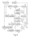
- FIG. 9 represents an embodiment of such a precorrection device with selective efficiency, universal, that is to say selectively covering the entire frequency band of the video signal.
- FIG. 3 Like that shown in FIG. 3, it includes an input distributor 1, one output of which is connected to a broadband channel comprising a delay line 2.
- the distributor also has three other outputs connected to the inputs of three selective correction channels, one at low frequency, comprising a delay line 20, and a low-pass filter 3 connected to an inverting amplifier 40 and to a non-inverting amplifier 41.
- the outputs of these amplifiers are connected to threshold correcting circuits 70 and 71, the outputs of which are connected to an adder 80.
- the output signal of the summator 80 is the precorrection signal to be superimposed on the signal of the broadband channel in the output summator 8, the part of this signal coming from the inverting amplifier performing a precorrection by compression, while the part of the signal from the non-inverting amplifier performs expansion correction.
- a second correction channel at mid frequencies, comprises a delay line 21, a bandpass filter 31 connected to the first input of a modulator, in a ring for example, 91.
- the second input of this modulator receives a signal modulation to model the amplitude of the signal selected by the bandpass filter.
- the outputs of amplifiers 40 and 41 are connected to the inputs of two threshold correcting circuits, 72 and 73, selecting for each direction of correction the range of levels to be corrected for the signal at mid frequencies and making it possible to adjust the efficiency. of the correction.
- These two correcting circuits are connected to the inputs of a summator 81, the output of which is connected to the second input of the modulator 91, its output being connected to a third input of the output summator, 8.
- a third correction channel at "high" frequencies comprises a delay line 22, a high-pass filter 32 connected to a ring modulator, 92 the output of which is connected to the fourth input of the output summator 8
- Two correcting circuits 74 and 75 are connected to the inverting 40 and non-inverting amplifiers 41 respectively, their outputs being connected to an adder 82 whose output is connected to the second input of the modulator 92.
- the delay lines placed in each of the channels make it possible to make up for the offsets that may occur between the channels due to the filters.
- Such a correction device makes it possible to act selectively on the video frequency signal by carrying out for example a compression of the average levels of the luminance signal, at the same time as an expansion of these same average levels in the band of the subcarrier of chromi nance or any other combination of expansion or compression with adjustable efficiency in the frequency bands determined by the filters.
- This type of frequency-selective amplitude correction device with frequency-selective efficiency is particularly applicable to television transmitters carrying out a separate amplification of the image and sound carrier channels, or to television transmitters carrying out a reduced carrier amplification in the image channel. However, it can also be used in television transmitters for common channel amplification, as a complement to a third-order intermodulation corrector.
- a correction circuit of the type described with reference to FIG. 7 is applicable to correct the so-called "S" distortions.
- Such a correction circuit can also be used in television cameras and in all the equipment where processing of the video frequency signal is necessary.
- the embodiment in which only one action zone is selected can be used as a white limitation circuit, by suitably choosing the values of the elements of the output circuit, R 4 , R 5 and R 6 in the figure. 4.
Landscapes
- Engineering & Computer Science (AREA)
- Multimedia (AREA)
- Signal Processing (AREA)
- Picture Signal Circuits (AREA)
- Cable Transmission Systems, Equalization Of Radio And Reduction Of Echo (AREA)
Priority Applications (1)
| Application Number | Priority Date | Filing Date | Title |
|---|---|---|---|
| AT82400614T ATE11354T1 (de) | 1981-04-14 | 1982-04-02 | Vorrichtung zur korrektur nichtlinearer videofrequenz mit selektiver zweckmaessigkeit. |
Applications Claiming Priority (2)
| Application Number | Priority Date | Filing Date | Title |
|---|---|---|---|
| FR8107459 | 1981-04-14 | ||
| FR8107459A FR2503970B1 (fr) | 1981-04-14 | 1981-04-14 | Dispositif de correction de non-linearite videofrequence a efficacite selective et equipement de television comportant un tel dispositif |
Publications (2)
| Publication Number | Publication Date |
|---|---|
| EP0064431A1 true EP0064431A1 (de) | 1982-11-10 |
| EP0064431B1 EP0064431B1 (de) | 1985-01-16 |
Family
ID=9257375
Family Applications (1)
| Application Number | Title | Priority Date | Filing Date |
|---|---|---|---|
| EP82400614A Expired EP0064431B1 (de) | 1981-04-14 | 1982-04-02 | Vorrichtung zur Korrektur nichtlinearer Videofrequenz mit selektiver Zweckmässigkeit |
Country Status (10)
| Country | Link |
|---|---|
| US (1) | US4502076A (de) |
| EP (1) | EP0064431B1 (de) |
| JP (1) | JPS57180239A (de) |
| AR (1) | AR229121A1 (de) |
| AT (1) | ATE11354T1 (de) |
| AU (1) | AU548666B2 (de) |
| CA (1) | CA1199102A (de) |
| DE (1) | DE3261911D1 (de) |
| FR (1) | FR2503970B1 (de) |
| MX (1) | MX151387A (de) |
Cited By (1)
| Publication number | Priority date | Publication date | Assignee | Title |
|---|---|---|---|---|
| EP0731602A1 (de) * | 1995-03-09 | 1996-09-11 | Telediffusion De France | Fernsehkanal mit einem Datenkanal |
Families Citing this family (6)
| Publication number | Priority date | Publication date | Assignee | Title |
|---|---|---|---|---|
| US4573081A (en) * | 1983-08-26 | 1986-02-25 | Rca Corporation | Frequency selective video signal compression |
| DE3517697A1 (de) * | 1985-05-17 | 1986-11-20 | Robert Bosch Gmbh, 7000 Stuttgart | Verfahren zur wiedereinfuehrung der exakten phasenbeziehung eines chrominanzsignals zu einem vorgegebenen referenztraegersignal |
| DE19529267B4 (de) * | 1995-08-09 | 2004-04-08 | Rohde & Schwarz Gmbh & Co. Kg | Kompensationsanordnung für einen Fernseh-HF-Leistungsverstärker |
| US5847772A (en) * | 1996-09-11 | 1998-12-08 | Wells; Aaron | Adaptive filter for video processing applications |
| GB0020280D0 (en) * | 2000-08-18 | 2000-10-04 | Vlsi Vision Ltd | Modification of column fixed pattern column noise in solid image sensors |
| US6755281B2 (en) | 2002-01-13 | 2004-06-29 | Intex Recreation Corp. | Swimming pool ladder |
Citations (1)
| Publication number | Priority date | Publication date | Assignee | Title |
|---|---|---|---|---|
| FR2301133A1 (fr) * | 1975-02-14 | 1976-09-10 | Thomson Csf | Dispo |
Family Cites Families (3)
| Publication number | Priority date | Publication date | Assignee | Title |
|---|---|---|---|---|
| US3975586A (en) * | 1975-06-16 | 1976-08-17 | The United States Of America As Represnted By The Secretary Of The Army | Automatic low frequency gain limited circuit for eliminating signal suppression in an A-C coupled video processing system |
| DE2921246A1 (de) * | 1979-05-25 | 1980-12-04 | Bosch Gmbh Robert | Verfahren und schaltung zur kontrastkorrektur von farbfernsehsignalen |
| US4388638A (en) * | 1981-01-19 | 1983-06-14 | Rca Corporation | De-emphasis for digitized composite color television signals |
-
1981
- 1981-04-14 FR FR8107459A patent/FR2503970B1/fr not_active Expired
-
1982
- 1982-04-02 AT AT82400614T patent/ATE11354T1/de not_active IP Right Cessation
- 1982-04-02 DE DE8282400614T patent/DE3261911D1/de not_active Expired
- 1982-04-02 EP EP82400614A patent/EP0064431B1/de not_active Expired
- 1982-04-05 US US06/365,388 patent/US4502076A/en not_active Expired - Fee Related
- 1982-04-12 AR AR289070A patent/AR229121A1/es active
- 1982-04-13 MX MX192245A patent/MX151387A/es unknown
- 1982-04-13 CA CA000400886A patent/CA1199102A/en not_active Expired
- 1982-04-14 AU AU82589/82A patent/AU548666B2/en not_active Ceased
- 1982-04-14 JP JP57061186A patent/JPS57180239A/ja active Granted
Patent Citations (1)
| Publication number | Priority date | Publication date | Assignee | Title |
|---|---|---|---|---|
| FR2301133A1 (fr) * | 1975-02-14 | 1976-09-10 | Thomson Csf | Dispo |
Non-Patent Citations (1)
| Title |
|---|
| TELECOMMUNICATIONS AND RADIO ENGINEERING, volume 29/30, no. 11, novembre 1975,WASHINGTON (US) V.I. SHCHURSKIY: "Correction of differential-phase distortion in TV transmitters", pages 12 à 19 * |
Cited By (2)
| Publication number | Priority date | Publication date | Assignee | Title |
|---|---|---|---|---|
| EP0731602A1 (de) * | 1995-03-09 | 1996-09-11 | Telediffusion De France | Fernsehkanal mit einem Datenkanal |
| FR2731576A1 (fr) * | 1995-03-09 | 1996-09-13 | Telediffusion Fse | Chaine d'emission de signaux de television comportant une voie de donnees |
Also Published As
| Publication number | Publication date |
|---|---|
| DE3261911D1 (en) | 1985-02-28 |
| US4502076A (en) | 1985-02-26 |
| FR2503970B1 (fr) | 1985-10-18 |
| JPS57180239A (en) | 1982-11-06 |
| JPH0262971B2 (de) | 1990-12-27 |
| CA1199102A (en) | 1986-01-07 |
| FR2503970A1 (fr) | 1982-10-15 |
| AU8258982A (en) | 1982-10-21 |
| MX151387A (es) | 1984-11-13 |
| EP0064431B1 (de) | 1985-01-16 |
| ATE11354T1 (de) | 1985-02-15 |
| AU548666B2 (en) | 1986-01-02 |
| AR229121A1 (es) | 1983-06-15 |
Similar Documents
| Publication | Publication Date | Title |
|---|---|---|
| EP0040127A1 (de) | Signalübertragungsanordnung mit einer Schaltung zur Vorkorrektur nichtlinearer Produkte | |
| EP0192497B1 (de) | Einrichtung zum Reduzieren der Dynamik der drei Farbbildsignale | |
| FR2596604A1 (fr) | Appareil de reglage automatique du gain dans le canal du son d'un systeme de traitement d'un signal video brouille | |
| EP0064431B1 (de) | Vorrichtung zur Korrektur nichtlinearer Videofrequenz mit selektiver Zweckmässigkeit | |
| FR2576733A1 (fr) | Systeme de surimpression d'images | |
| EP0010023B1 (de) | Leistungstarkes Amplitudenmodulationsübertragungssystem und Fernsehsender und -relaissender, die ein ähnliches System enthalten | |
| EP0169093B1 (de) | Empfänger für Fernsehzeitmultiplexübertragung mit einem Frequenzdemodulator | |
| EP0141715B1 (de) | Vorrichtung zur automatischen Vorkorrektur von Nichtlinearitäten in einer Leistungsverstärkerkette, sowie ihre Anwendung in einem Fernsehsender | |
| EP0081413B1 (de) | Retransmissionseinrichtung mit gemeinsamer Bild-/Tonträgerverstärkung und automatischer Steuerung des Bild-/Tonverhältnisses | |
| FR2507846A1 (fr) | Perfectionnement a un recepteur sans fil | |
| FR2698174A1 (fr) | Procédé de mesure du rapport signal-sur-bruit dans un amplificateur. | |
| FR2519174A1 (fr) | Circuit de reduction de bruit | |
| EP0086124B1 (de) | Anordnung zur Korrektur der Nichtlinearität durch Zwischenfrequenz-Vormodulation in einer Fernseheinrichtung | |
| EP0028181B1 (de) | Vorrichtung zur Hochfrequenz-Vorkorrektur der Nichtlinearität in Signalverstärkern, wobei das Signal mindestens ein amplitudemoduliertes Trägersignal umfasst, und diese Vorrichtung enthaltender Fernsehsender | |
| EP0071294B1 (de) | Frequenzdemodulator | |
| EP0711034B1 (de) | Vorrichtung zum Generieren von Übertragungsfunktionen in Segmenten | |
| EP0562963B1 (de) | Verfahren zur Verstärkungsregelung in einem Empfänger für Datensignale | |
| EP0057117B1 (de) | Leuchtdichtesignal-Begrenzereinrichtung | |
| FR2472322A1 (fr) | Dispositif de mesure, en exploitation, de produits de non linearite et emetteur et/ou reemetteur de television comportant un tel dispositif | |
| FR2538141A1 (fr) | Dispositif de limitation de l'amplitude d'un signal par ecretage superieur et inferieur | |
| FR2469829A1 (fr) | Amplificateur a large bande avec commande automatique de gain, sequentielle et frequentielle | |
| JPH05268169A (ja) | 光受信装置 | |
| FR2618032A1 (fr) | Circuit filtre cloche et contre-cloche | |
| FR2469844A1 (fr) | Dispositif de reception de signaux de television | |
| FR2546353A1 (fr) | Dispositif de correction anti-halo pour tube analyseur de camera de television |
Legal Events
| Date | Code | Title | Description |
|---|---|---|---|
| PUAI | Public reference made under article 153(3) epc to a published international application that has entered the european phase |
Free format text: ORIGINAL CODE: 0009012 |
|
| AK | Designated contracting states |
Designated state(s): AT BE CH DE GB NL SE |
|
| 17P | Request for examination filed |
Effective date: 19830321 |
|
| RAP1 | Party data changed (applicant data changed or rights of an application transferred) |
Owner name: THOMSON-LGT LABORATOIRE GENERAL DES TELECOMMUNICAT |
|
| GRAA | (expected) grant |
Free format text: ORIGINAL CODE: 0009210 |
|
| AK | Designated contracting states |
Designated state(s): AT BE CH DE GB LI NL SE |
|
| REF | Corresponds to: |
Ref document number: 11354 Country of ref document: AT Date of ref document: 19850215 Kind code of ref document: T |
|
| REF | Corresponds to: |
Ref document number: 3261911 Country of ref document: DE Date of ref document: 19850228 |
|
| PLBE | No opposition filed within time limit |
Free format text: ORIGINAL CODE: 0009261 |
|
| STAA | Information on the status of an ep patent application or granted ep patent |
Free format text: STATUS: NO OPPOSITION FILED WITHIN TIME LIMIT |
|
| 26N | No opposition filed | ||
| PGFP | Annual fee paid to national office [announced via postgrant information from national office to epo] |
Ref country code: AT Payment date: 19860430 Year of fee payment: 5 |
|
| PGFP | Annual fee paid to national office [announced via postgrant information from national office to epo] |
Ref country code: NL Payment date: 19870430 Year of fee payment: 6 |
|
| PG25 | Lapsed in a contracting state [announced via postgrant information from national office to epo] |
Ref country code: AT Effective date: 19880402 |
|
| PG25 | Lapsed in a contracting state [announced via postgrant information from national office to epo] |
Ref country code: NL Effective date: 19881101 |
|
| NLV4 | Nl: lapsed or anulled due to non-payment of the annual fee | ||
| EAL | Se: european patent in force in sweden |
Ref document number: 82400614.2 |
|
| PGFP | Annual fee paid to national office [announced via postgrant information from national office to epo] |
Ref country code: CH Payment date: 19960315 Year of fee payment: 15 |
|
| PGFP | Annual fee paid to national office [announced via postgrant information from national office to epo] |
Ref country code: GB Payment date: 19960319 Year of fee payment: 15 |
|
| PGFP | Annual fee paid to national office [announced via postgrant information from national office to epo] |
Ref country code: DE Payment date: 19960320 Year of fee payment: 15 |
|
| PGFP | Annual fee paid to national office [announced via postgrant information from national office to epo] |
Ref country code: SE Payment date: 19960321 Year of fee payment: 15 |
|
| PGFP | Annual fee paid to national office [announced via postgrant information from national office to epo] |
Ref country code: BE Payment date: 19960409 Year of fee payment: 15 |
|
| PG25 | Lapsed in a contracting state [announced via postgrant information from national office to epo] |
Ref country code: GB Effective date: 19970402 |
|
| PG25 | Lapsed in a contracting state [announced via postgrant information from national office to epo] |
Ref country code: SE Effective date: 19970403 |
|
| PG25 | Lapsed in a contracting state [announced via postgrant information from national office to epo] |
Ref country code: LI Free format text: LAPSE BECAUSE OF NON-PAYMENT OF DUE FEES Effective date: 19970430 Ref country code: CH Free format text: LAPSE BECAUSE OF NON-PAYMENT OF DUE FEES Effective date: 19970430 Ref country code: BE Effective date: 19970430 |
|
| BERE | Be: lapsed |
Owner name: THOMSON-LGT LABORATOIRE GENERAL DES TELECOMMUNICA Effective date: 19970430 |
|
| GBPC | Gb: european patent ceased through non-payment of renewal fee |
Effective date: 19970402 |
|
| REG | Reference to a national code |
Ref country code: CH Ref legal event code: PL |
|
| PG25 | Lapsed in a contracting state [announced via postgrant information from national office to epo] |
Ref country code: DE Free format text: LAPSE BECAUSE OF NON-PAYMENT OF DUE FEES Effective date: 19980101 |
|
| EUG | Se: european patent has lapsed |
Ref document number: 82400614.2 |