EP0064513B1 - Circuit de reference a courant de polarisation - Google Patents
Circuit de reference a courant de polarisation Download PDFInfo
- Publication number
- EP0064513B1 EP0064513B1 EP81902994A EP81902994A EP0064513B1 EP 0064513 B1 EP0064513 B1 EP 0064513B1 EP 81902994 A EP81902994 A EP 81902994A EP 81902994 A EP81902994 A EP 81902994A EP 0064513 B1 EP0064513 B1 EP 0064513B1
- Authority
- EP
- European Patent Office
- Prior art keywords
- bias
- voltage
- transistor
- current
- bias current
- Prior art date
- Legal status (The legal status is an assumption and is not a legal conclusion. Google has not performed a legal analysis and makes no representation as to the accuracy of the status listed.)
- Expired
Links
- 238000004519 manufacturing process Methods 0.000 description 3
- 238000000034 method Methods 0.000 description 3
- 230000015556 catabolic process Effects 0.000 description 1
- 230000000295 complement effect Effects 0.000 description 1
Images
Classifications
-
- G—PHYSICS
- G05—CONTROLLING; REGULATING
- G05F—SYSTEMS FOR REGULATING ELECTRIC OR MAGNETIC VARIABLES
- G05F3/00—Non-retroactive systems for regulating electric variables by using an uncontrolled element, or an uncontrolled combination of elements, such element or such combination having self-regulating properties
- G05F3/02—Regulating voltage or current
- G05F3/08—Regulating voltage or current wherein the variable is DC
- G05F3/10—Regulating voltage or current wherein the variable is DC using uncontrolled devices with non-linear characteristics
- G05F3/16—Regulating voltage or current wherein the variable is DC using uncontrolled devices with non-linear characteristics being semiconductor devices
- G05F3/20—Regulating voltage or current wherein the variable is DC using uncontrolled devices with non-linear characteristics being semiconductor devices using diode- transistor combinations
- G05F3/26—Current mirrors
- G05F3/267—Current mirrors using both bipolar and field-effect technology
Definitions
- This invention relates generally to reference circuits and, more particularly, to a circuit which provides reference voltages for bias current generators and the like.
- bias reference circuits can be classified by the source of the voltage standard by which the bias currents are established. As noted in Analysis and Design of Analog Integrated Circuits by Paul R. Grey and Robert G. Meyer (John Wiley & Sons, 1977, pages 239-261), the most convenient standards are the V BE of a transistor, the thermal voltage, V T , and the breakdown voltage of a reverse-biased emitter-base junction of a transistor. While each of these voltage reference elements may be readily fabricated using conventional bipolar integrated circuit fabrication processes, it is significantly more difficult to fabricate the open-collector bipolar devices utilized in common V BE reference circuits using conventional MOS integrated circuit fabrication processes.
- the reverse-biased emitter-base junction or Zener diode reference circuit although manufacturable in most MOS fabrication processes, generally requires supply voltages exceeding 7 to 8 volts, and tends to introduce significant amounts of noise under reverse-breakdown conditions.
- An object of an embodiment of the present invention is to provide a self-biasing MOS bias current reference circuit capable of generating complementary bias voltages even when used with relatively low supply voltages.
- a bias current reference circuit comprising:
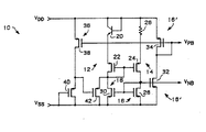
- the Figure illustrates in schematic form a bias current reference circuit constructed in accordance with the preferred embodiment of the present invention.
- the reference circuit 10 is comprised generally of a reference voltage portion 12, a reference current portion 14, a bias voltage portion 16 and a bias current portion 18.
- an NPN bipolar transistor 20 has the base and collector thereof connected to a positive supply V DD , and the emitter thereof connected to the source of a P-channel MOS transistor 22 which has the gate and drain thereof connected to the reference current portion 14 and to the bias current portion 18. In this configuration, a reference voltage with respect to the positive supply .
- V DD will be developed on the gate of-the transistor 22 which is the sum of the V Be of the diode-connected transistor 20 and the V GS of the diode-connected transistor 22, the latter being proportional to a bias current directed therethrough by the bias current portion 18.
- a P-channel MOS transistor 24 has the source thereof connected to the positive supply V oo via a resistor 26, the gate thereof connected to the gate and drain of the transistor 22, and the drain thereof connected to the bias voltage portion 16.
- the gate to source voltage V GS of the transistor 24 will be substantially the same as that of the transistor 22.
- the base-emitter voltage V BE of the transistor 20 will be reflected across the resistor 26.
- the reference current portion 14 will therefore provide a reference current which is proportional to the reference voltage provided by the reference voltage portion 12.
- an N-channel MOS transistor 28 has the source thereof connected to a negative supply V ss , and the gate and drain thereof connected to the drain of the transistor 24 of the reference current portion 14.
- V ss negative supply
- the-diode-connected transistor 28 will develop a gate to source voltage V GS which is proportional to the reference current.
- V NB' is suitable for biasing other N-channel MOS transistors used as constant bias current sinks.
- an N-channel MOS transistor 30 as the source thereof connected to the negative supply V ss , the gate thereof connected to the gate and drain of the transistor 28, and the drain thereof connected to the gate and drain of the transistor 22.
- the transistor 30 will allow a bias current proportional to the bias voltage V NB to flow through the transistors 20 and 22 of the reference voltage portion 12.
- a P-channel bias voltage V PB as a counterpart for the N-channel bias voltage V NB .
- this is accomplished using a second bias current portion 18' and a - second bias voltage portion 16'.
- an N-channel MOS transistor 32 has the source thereof connected to the negative supply V ss , the gate thereof connected to the gate and drain of the transistor 28 of.the bias voltage portion 16, and the drain thereof connected to the second bias voltage portion 16'.
- a P-channel MOS transistor 34 has the gate and drain thereof connected to the drain of the transistor 32, and the source thereof connected to the positive supply V DD .
- the transistor 32 will allow a bias current proportional to the N-channel bias voltage V NB to flow through the transistor 34.
- the diode-connected transistor 34 develops a gate to source voltage V ss which is proportional to the bias current, but referenced to the positive supply V DD rather than the negative supply V ss .
- This voltage indicated as V PB , is suitable for biasing other P-channel MOS transistors used as constant current sources.
- the bias current reference circuit 10 may assume either an inactive or an active state. For example, if no current flows through the reference voltage portion 12 during power up, no reference voltage will be developed for application to the reference current portion 14. Thus, no reference current will be provided by the reference current portion 14. Without reference current, the bias voltage portion 16 will be unable to establish the bias voltage V NB and enable the bias current portion 18 to direct bias current through the reference voltage portion 12. The bias current reference circuit 10 will therefore remain in the inactive state.
- a start-up portion 36 is provided to allow start-up current to flow through the reference voltage portion 12 when the P-channel bias voltage V PB with respect to the positive supply V DD is less than a predetermined threshold.
- a P-channel MOS transistor 38 has the source thereof connected to the positive supply V DD and the gate thereof connected to the gate and drain of the transistor 34 of the second bias voltage portion 16'.
- the drain of the transistor 38 is connected to the source of a P-channel MOS transistor 40 which has the gate and drain thereof connected to the negative supply V ss .
- the drain of the transistor 38 is also connected to the gate of a P-channel MOS transistor 42 which has the source thereof connected to the gate and drain of the transistor 22, and the drain thereof connected to the negative supply V ss .
- the transistor 38 provides bias current for the diode-connected transistor 40 only when the P-channel bias voltage Vp B applied to the gate of the transistor 38 is at least one V GS below the positive supply V DD .
- the transistor 40 By constructing the transistor 40 to have a smaller ratio of channel width to channel length than the transistor 38 and thus a higher current density, the gate to source voltage V GS of the transistor 40 will be relatively high when the transistor 38 is turned on.
- the transistor 42 will be turned on only when the transistor 38 is turned off, i.e. when the bias current reference circuit 10 is in the passive state.
- the transistor 42 turns on, the voltage on the gate and drain of the transistor 22 of the reference voltage portion 12 is pulled toward the negative supply Vss.
- the transistor 32 With the N-channel bias voltage V Ns established, the transistor 32 provides a path for current to flow through the transistor 34.
- the transistor 34 being diode-connected, establishes the P-channel bias voltage Vp B one V GS below the positive supply V DD .
- the transistor 38 turns the transistor 42 off by pulling the gate thereof toward the positive supply V DD .
- the start-up portion 36 becomes inactive once the bias current reference circuit 10 assumes the active state.
- the start-up portion 36 automatically becomes active if, for any reason, the bias current reference circuit 10 should try to return to the inactive state.
Landscapes
- Engineering & Computer Science (AREA)
- Physics & Mathematics (AREA)
- Microelectronics & Electronic Packaging (AREA)
- Nonlinear Science (AREA)
- Electromagnetism (AREA)
- General Physics & Mathematics (AREA)
- Radar, Positioning & Navigation (AREA)
- Automation & Control Theory (AREA)
- Control Of Electrical Variables (AREA)
Claims (6)
Applications Claiming Priority (2)
| Application Number | Priority Date | Filing Date | Title |
|---|---|---|---|
| US06/207,532 US4342926A (en) | 1980-11-17 | 1980-11-17 | Bias current reference circuit |
| US207532 | 2002-07-29 |
Publications (3)
| Publication Number | Publication Date |
|---|---|
| EP0064513A1 EP0064513A1 (fr) | 1982-11-17 |
| EP0064513A4 EP0064513A4 (fr) | 1983-03-23 |
| EP0064513B1 true EP0064513B1 (fr) | 1986-04-23 |
Family
ID=22770981
Family Applications (1)
| Application Number | Title | Priority Date | Filing Date |
|---|---|---|---|
| EP81902994A Expired EP0064513B1 (fr) | 1980-11-17 | 1981-10-23 | Circuit de reference a courant de polarisation |
Country Status (5)
| Country | Link |
|---|---|
| US (1) | US4342926A (fr) |
| EP (1) | EP0064513B1 (fr) |
| JP (1) | JPS57501753A (fr) |
| CA (1) | CA1160698A (fr) |
| WO (1) | WO1982001776A1 (fr) |
Families Citing this family (38)
| Publication number | Priority date | Publication date | Assignee | Title |
|---|---|---|---|---|
| FR2494519A1 (fr) * | 1980-11-14 | 1982-05-21 | Efcis | Generateur de courant integre en technologie cmos |
| US4450367A (en) * | 1981-12-14 | 1984-05-22 | Motorola, Inc. | Delta VBE bias current reference circuit |
| US4464588A (en) * | 1982-04-01 | 1984-08-07 | National Semiconductor Corporation | Temperature stable CMOS voltage reference |
| US4472647A (en) * | 1982-08-20 | 1984-09-18 | Motorola, Inc. | Circuit for interfacing with both TTL and CMOS voltage levels |
| US4461991A (en) * | 1983-02-28 | 1984-07-24 | Motorola, Inc. | Current source circuit having reduced error |
| US4532467A (en) * | 1983-03-14 | 1985-07-30 | Vitafin N.V. | CMOS Circuits with parameter adapted voltage regulator |
| US4585961A (en) * | 1984-01-19 | 1986-04-29 | At&T Bell Laboratories | Semiconductor integrated circuit for squaring a signal with suppression of the linear component |
| US4723108A (en) * | 1986-07-16 | 1988-02-02 | Cypress Semiconductor Corporation | Reference circuit |
| US4792748A (en) * | 1987-11-17 | 1988-12-20 | Burr-Brown Corporation | Two-terminal temperature-compensated current source circuit |
| US4820967A (en) * | 1988-02-02 | 1989-04-11 | National Semiconductor Corporation | BiCMOS voltage reference generator |
| JPH0727424B2 (ja) * | 1988-12-09 | 1995-03-29 | 富士通株式会社 | 定電流源回路 |
| US5029283A (en) * | 1990-03-28 | 1991-07-02 | Ncr Corporation | Low current driver for gate array |
| JP2978226B2 (ja) * | 1990-09-26 | 1999-11-15 | 三菱電機株式会社 | 半導体集積回路 |
| US5045773A (en) * | 1990-10-01 | 1991-09-03 | Motorola, Inc. | Current source circuit with constant output |
| US5179297A (en) * | 1990-10-22 | 1993-01-12 | Gould Inc. | CMOS self-adjusting bias generator for high voltage drivers |
| US5155384A (en) * | 1991-05-10 | 1992-10-13 | Samsung Semiconductor, Inc. | Bias start-up circuit |
| KR940004026Y1 (ko) * | 1991-05-13 | 1994-06-17 | 금성일렉트론 주식회사 | 바이어스의 스타트업회로 |
| US5245273A (en) * | 1991-10-30 | 1993-09-14 | Motorola, Inc. | Bandgap voltage reference circuit |
| JP2953226B2 (ja) * | 1992-12-11 | 1999-09-27 | 株式会社デンソー | 基準電圧発生回路 |
| JP3318105B2 (ja) * | 1993-08-17 | 2002-08-26 | 三菱電機株式会社 | 起動回路 |
| JP3436971B2 (ja) * | 1994-06-03 | 2003-08-18 | 三菱電機株式会社 | 電圧制御型電流源およびそれを用いたバイアス発生回路 |
| FR2732129B1 (fr) * | 1995-03-22 | 1997-06-20 | Suisse Electronique Microtech | Generateur de courant de reference en technologie cmos |
| KR0142970B1 (ko) * | 1995-06-24 | 1998-08-17 | 김광호 | 반도체 메모리 장치의 기준전압 발생회로 |
| KR100237623B1 (ko) * | 1996-10-24 | 2000-01-15 | 김영환 | 기준 전압 회로의 전류 감지 스타트 업 회로 |
| JP3476363B2 (ja) * | 1998-06-05 | 2003-12-10 | 日本電気株式会社 | バンドギャップ型基準電圧発生回路 |
| DE19940382A1 (de) * | 1999-08-25 | 2001-03-08 | Infineon Technologies Ag | Stromquelle für niedrige Betriebsspannungen mit hohem Ausgangswiderstand |
| US6346803B1 (en) * | 2000-11-30 | 2002-02-12 | Intel Corporation | Current reference |
| US6433624B1 (en) | 2000-11-30 | 2002-08-13 | Intel Corporation | Threshold voltage generation circuit |
| US6342781B1 (en) | 2001-04-13 | 2002-01-29 | Ami Semiconductor, Inc. | Circuits and methods for providing a bandgap voltage reference using composite resistors |
| US6351111B1 (en) | 2001-04-13 | 2002-02-26 | Ami Semiconductor, Inc. | Circuits and methods for providing a current reference with a controlled temperature coefficient using a series composite resistor |
| US6734719B2 (en) * | 2001-09-13 | 2004-05-11 | Kabushiki Kaisha Toshiba | Constant voltage generation circuit and semiconductor memory device |
| US6693332B2 (en) * | 2001-12-19 | 2004-02-17 | Intel Corporation | Current reference apparatus |
| US20050003764A1 (en) * | 2003-06-18 | 2005-01-06 | Intel Corporation | Current control circuit |
| JP4374254B2 (ja) * | 2004-01-27 | 2009-12-02 | Okiセミコンダクタ株式会社 | バイアス電圧発生回路 |
| US7091712B2 (en) * | 2004-05-12 | 2006-08-15 | Freescale Semiconductor, Inc. | Circuit for performing voltage regulation |
| US7816975B2 (en) * | 2005-09-20 | 2010-10-19 | Hewlett-Packard Development Company, L.P. | Circuit and method for bias voltage generation |
| US7554313B1 (en) | 2006-02-09 | 2009-06-30 | National Semiconductor Corporation | Apparatus and method for start-up circuit without a start-up resistor |
| CN101526826B (zh) * | 2008-03-04 | 2011-11-30 | 亿而得微电子股份有限公司 | 参考电压产生装置 |
Family Cites Families (11)
| Publication number | Priority date | Publication date | Assignee | Title |
|---|---|---|---|---|
| US3823332A (en) * | 1970-01-30 | 1974-07-09 | Rca Corp | Mos fet reference voltage supply |
| US3806742A (en) * | 1972-11-01 | 1974-04-23 | Motorola Inc | Mos voltage reference circuit |
| US3922596A (en) * | 1973-08-13 | 1975-11-25 | Motorola Inc | Current regulator |
| US4032839A (en) * | 1975-08-26 | 1977-06-28 | Rca Corporation | Current scaling circuits |
| US4009432A (en) * | 1975-09-04 | 1977-02-22 | Rca Corporation | Constant current supply |
| JPS5849885B2 (ja) * | 1976-03-16 | 1983-11-07 | 日本電気株式会社 | 定電圧回路 |
| US4096430A (en) * | 1977-04-04 | 1978-06-20 | General Electric Company | Metal-oxide-semiconductor voltage reference |
| DE2826624C2 (de) * | 1978-06-19 | 1982-11-04 | Deutsche Itt Industries Gmbh, 7800 Freiburg | Integrierte IGFET-Konstantstromquelle |
| US4302718A (en) * | 1980-05-27 | 1981-11-24 | Rca Corporation | Reference potential generating circuits |
| US4300091A (en) * | 1980-07-11 | 1981-11-10 | Rca Corporation | Current regulating circuitry |
| FR2494519A1 (fr) * | 1980-11-14 | 1982-05-21 | Efcis | Generateur de courant integre en technologie cmos |
-
1980
- 1980-11-17 US US06/207,532 patent/US4342926A/en not_active Expired - Lifetime
-
1981
- 1981-09-30 CA CA000387008A patent/CA1160698A/fr not_active Expired
- 1981-10-23 WO PCT/US1981/001423 patent/WO1982001776A1/fr not_active Ceased
- 1981-10-23 JP JP56503514A patent/JPS57501753A/ja active Pending
- 1981-10-23 EP EP81902994A patent/EP0064513B1/fr not_active Expired
Non-Patent Citations (1)
| Title |
|---|
| ELECTRONIC DESIGN, vol. 26, no 23, November 8, 1978, ROCHELLE PARK (US), D. Bingham: "CMOS: Higher Speeds, more drive and analog capability expand its horizons", pages 74-82 * |
Also Published As
| Publication number | Publication date |
|---|---|
| JPS57501753A (fr) | 1982-09-24 |
| EP0064513A1 (fr) | 1982-11-17 |
| EP0064513A4 (fr) | 1983-03-23 |
| WO1982001776A1 (fr) | 1982-05-27 |
| CA1160698A (fr) | 1984-01-17 |
| US4342926A (en) | 1982-08-03 |
Similar Documents
| Publication | Publication Date | Title |
|---|---|---|
| EP0064513B1 (fr) | Circuit de reference a courant de polarisation | |
| US4450367A (en) | Delta VBE bias current reference circuit | |
| US6987416B2 (en) | Low-voltage curvature-compensated bandgap reference | |
| US5059890A (en) | Constant current source circuit | |
| US7755344B2 (en) | Ultra low-voltage sub-bandgap voltage reference generator | |
| US6351111B1 (en) | Circuits and methods for providing a current reference with a controlled temperature coefficient using a series composite resistor | |
| US4810902A (en) | Logic interface circuit with high stability and low rest current | |
| US4935690A (en) | CMOS compatible bandgap voltage reference | |
| EP0155720B1 (fr) | Dispositif de source de courant en cascade | |
| US4119869A (en) | Constant current circuit | |
| US6842321B2 (en) | Supply independent low quiescent current undervoltage lockout circuit | |
| US4931718A (en) | CMOS voltage reference | |
| US6885179B1 (en) | Low-voltage bandgap reference | |
| USRE37778E1 (en) | Current limiting circuit | |
| US4433283A (en) | Band gap regulator circuit | |
| HK103288A (en) | Bias current reference circuit | |
| JP3349047B2 (ja) | 定電圧回路 | |
| US5966006A (en) | Voltage regulator generating a predetermined temperature-stable voltage | |
| US6054845A (en) | Current limiting circuit | |
| KR100292924B1 (ko) | 전류원 회로 | |
| EP0104777B1 (fr) | Circuit de source de courant constant | |
| US7952421B2 (en) | All NPN-transistor PTAT current source | |
| EP0885414B1 (fr) | Source de tension de reference a barriere de potentiel | |
| US5760631A (en) | Protection circuit for a CMOS integrated circuit | |
| US6215292B1 (en) | Method and device for generating an output current |
Legal Events
| Date | Code | Title | Description |
|---|---|---|---|
| PUAI | Public reference made under article 153(3) epc to a published international application that has entered the european phase |
Free format text: ORIGINAL CODE: 0009012 |
|
| 17P | Request for examination filed |
Effective date: 19820709 |
|
| AK | Designated contracting states |
Designated state(s): DE FR GB |
|
| GRAA | (expected) grant |
Free format text: ORIGINAL CODE: 0009210 |
|
| AK | Designated contracting states |
Kind code of ref document: B1 Designated state(s): DE FR GB |
|
| REF | Corresponds to: |
Ref document number: 3174479 Country of ref document: DE Date of ref document: 19860528 |
|
| ET | Fr: translation filed | ||
| PLBE | No opposition filed within time limit |
Free format text: ORIGINAL CODE: 0009261 |
|
| STAA | Information on the status of an ep patent application or granted ep patent |
Free format text: STATUS: NO OPPOSITION FILED WITHIN TIME LIMIT |
|
| 26N | No opposition filed | ||
| PGFP | Annual fee paid to national office [announced via postgrant information from national office to epo] |
Ref country code: GB Payment date: 19970930 Year of fee payment: 17 |
|
| PGFP | Annual fee paid to national office [announced via postgrant information from national office to epo] |
Ref country code: FR Payment date: 19971015 Year of fee payment: 17 |
|
| PGFP | Annual fee paid to national office [announced via postgrant information from national office to epo] |
Ref country code: DE Payment date: 19971023 Year of fee payment: 17 |
|
| PG25 | Lapsed in a contracting state [announced via postgrant information from national office to epo] |
Ref country code: GB Free format text: LAPSE BECAUSE OF NON-PAYMENT OF DUE FEES Effective date: 19981023 |
|
| GBPC | Gb: european patent ceased through non-payment of renewal fee |
Effective date: 19981023 |
|
| PG25 | Lapsed in a contracting state [announced via postgrant information from national office to epo] |
Ref country code: FR Free format text: LAPSE BECAUSE OF NON-PAYMENT OF DUE FEES Effective date: 19990630 |
|
| REG | Reference to a national code |
Ref country code: FR Ref legal event code: ST |
|
| PG25 | Lapsed in a contracting state [announced via postgrant information from national office to epo] |
Ref country code: DE Free format text: LAPSE BECAUSE OF NON-PAYMENT OF DUE FEES Effective date: 19990803 |