EP0065062A2 - Procédé pour la génération de signaux numériques périodiques de fonction de temps - Google Patents
Procédé pour la génération de signaux numériques périodiques de fonction de temps Download PDFInfo
- Publication number
- EP0065062A2 EP0065062A2 EP82100055A EP82100055A EP0065062A2 EP 0065062 A2 EP0065062 A2 EP 0065062A2 EP 82100055 A EP82100055 A EP 82100055A EP 82100055 A EP82100055 A EP 82100055A EP 0065062 A2 EP0065062 A2 EP 0065062A2
- Authority
- EP
- European Patent Office
- Prior art keywords
- time function
- signal
- period
- signals
- clock signal
- Prior art date
- Legal status (The legal status is an assumption and is not a legal conclusion. Google has not performed a legal analysis and makes no representation as to the accuracy of the status listed.)
- Granted
Links
- 238000000034 method Methods 0.000 title claims abstract description 20
- 230000000737 periodic effect Effects 0.000 title claims abstract description 8
- 230000006870 function Effects 0.000 claims abstract description 71
- 230000015654 memory Effects 0.000 claims abstract description 50
- 238000011156 evaluation Methods 0.000 claims description 16
- 230000003111 delayed effect Effects 0.000 claims description 2
- 238000010586 diagram Methods 0.000 description 5
- 241000233805 Phoenix Species 0.000 description 1
- 238000004590 computer program Methods 0.000 description 1
- 238000007620 mathematical function Methods 0.000 description 1
- 239000003208 petroleum Substances 0.000 description 1
- 239000010453 quartz Substances 0.000 description 1
- 239000004065 semiconductor Substances 0.000 description 1
- VYPSYNLAJGMNEJ-UHFFFAOYSA-N silicon dioxide Inorganic materials O=[Si]=O VYPSYNLAJGMNEJ-UHFFFAOYSA-N 0.000 description 1
- 230000001360 synchronised effect Effects 0.000 description 1
Images
Classifications
-
- H—ELECTRICITY
- H03—ELECTRONIC CIRCUITRY
- H03K—PULSE TECHNIQUE
- H03K5/00—Manipulating of pulses not covered by one of the other main groups of this subclass
- H03K5/15—Arrangements in which pulses are delivered at different times at several outputs, i.e. pulse distributors
- H03K5/15006—Arrangements in which pulses are delivered at different times at several outputs, i.e. pulse distributors with two programmable outputs
-
- H—ELECTRICITY
- H03—ELECTRONIC CIRCUITRY
- H03K—PULSE TECHNIQUE
- H03K3/00—Circuits for generating electric pulses; Monostable, bistable or multistable circuits
- H03K3/78—Generating a single train of pulses having a predetermined pattern, e.g. a predetermined number
Definitions
- the invention relates to a method for generating digital periodic time function signals, each of which a certain number of memory cells of a read-only memory are assigned, in each of these memory cells. a digitally coded data value is stored and the memory cells are called up in series with the aid of a first clock signal.
- Time function signals of this type are e.g. as reference signals in coherence receivers for the reception of e.g. "Chirp" signals needed.
- a received signal which may be disturbed, is multiplied on the one hand by the reference signal itself and on the other hand by the reference signal which is phase-shifted by 90 ° for the purpose of detecting the useful signal and eliminating the interference component.
- a coherence receiver is described in US Pat. No. 3,937,899, column 2, line 49 to column 3, line 43, but for the relatively simple case that the reference signal is a pure sine or cosine function and is stored in amplitude in terms of amplitude is.
- the invention has for its object to generate digital periodic time function signals that have any digital form within their period T and that have a high resolution accuracy despite the relatively low memory requirement.
- the frequency accuracy with e.g. 40 kHz should e.g. be approximately 100 Hz.
- Another advantage of the invention is that the relatively long settling times of the read-only memory data have no disruptive influence on the generation of the time function signals.
- the data values of the time function signals are not stored in terms of amplitude but in terms of time in the memory cells.
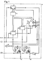
- a function generator 1 shown in FIG. 1 for generating two digital and periodic time function signals contains an address counter 2, a read-only memory 3, a first period counter 4, a second period counter 5, and a first one Signal flip-flop 6, a second signal flip-flop 7, a first "Nor” gate 8, a second "Nor” gate 9, a first inverter 10, a second inverter 11 and a logic circuit 12.
- the function generator 1 has a first, a second and a third clock input, which are fed in the specified order from an inverted first clock signal CL1, from a second clock signal CL2 and from an inverted third clock signal CL3. It also has a first signal output A for the first generated time function signal, e.g. a "1-chirp" signal, and a second signal output B for the second time function signal, e.g. an "O-Chirp" signal.
- the ground connection of the function generator 1 is connected via the inverter 11 to the respective set inputs P of the two signal flip-flops 6 and 7.
- the address counter 2 is a K-bit counter, the K outputs Q 1 , Q 2 , ..., Q K of which are led to the K-bit address input of the read-only memory 3 via a K-bit data bus.
- K 11.
- All remaining components of both FIG. 1 and FIG. 3 can be components of the "Low Power Schottky" series 74LS ... from Texas Instr., Dallas, Texas, USA.
- the N-bit data outputs Q 1 , Q 2 , ..., Q N * of the read-only memory 3 are with the help of N-bit data bus connections with the respective N-bit parallel input of the two period counters 4 and 5 and with the N-bit input of the Logic circuit 12 connected.
- 8-bit period counters 4 and 5 for example, two 4-bit binary counters, for example of the 74LS163 type, can be used in cascade connection, with their two "carry” outputs each leading to an additional, not shown "and” gate lead, the output of which forms the output of the period counter in question.
- the two time function signals generated in the function generator 1 are, for example, "chirp” signals, namely that a "1-chirp” signal appears at the first output A of the function generator 1, representing the value "logical 1", and a "1" at the second output B. O-Chirp “signal, representing the value” logic 0 ".
- the highest final frequency f E, i of the reference signal is approximately 40 kHz and the lowest initial frequency f B , i is selected, for example, equal to 10 kHz.
- the period T 3 of the third clock signal CL3 is equal to the period T of the time function signals and the duration of their pulses, for example approximately 1 ⁇ s or at least less than a quarter period T l of the first clock signal CL1.
- the third clock signal CL3 is synchronized with the network, for example with the aid of comparators, for example of the type LM311 from National Semiconductor, Santa Clara, California, USA, and a monostable multivibrator, for example of the type 74LS221, in a known and therefore not shown manner created.
- comparators for example of the type LM311 from National Semiconductor, Santa Clara, California, USA
- a monostable multivibrator for example of the type 74LS221
- the positive going edge of the third clock signal CL3 brings the function generator 1 back into the starting position by all signal flip-flops 6 and 7 directly, the address counter 2 via the inverter 10 and all release flip-flops Logic circuit 12 can also be reset to zero via the two "Nor" gates 8 and 9.
- the address counter 2 begins to count binary from the negative going edges of the inverted first clock signal CL1. These negative going edges of the inverted first clock signal CL1 correspond in time to the positive going edges of the non-inverted first clock signal CL1.
- the K-bit count of the address counter 2 increases continuously, and with it the K-bit value of the addresses of the read-only memory 3. These addresses successively and continuously call up the N-bit data values x j of all memory cells of the read-only memory 3.
- Certain memory cells of the read-only memory 3 are assigned to each of the two function signals. Because the ark Input "Load" of the two period counters 4 and 5 is at logic "0", as will be explained later with reference to FIG. 3, these N-bit data values x.
- a half period T is selected to the first clock signal CL1 half as time delay. This time delay is taken into account in advance when creating the data for the read-only memory 3.
- a logical "1" appears at the output of the relevant period counter 4 or 5, which on the one hand blocks the logic circuit 12 and thus the evaluation of the period counter 4 or 5 again via one of the two “Nor” gates 8 or 9 and on the other hand, with its positive going edge, switches the signal flip-flop 6 or 7 belonging to the relevant period counter 4 or 5 and fed back from Q to D. This changes the value of its Q output signal at the right moment.
- This Q The output signal is at the same time the associated time function signal which appeared at the relevant signal output A or B of the function generator 1 and which was to be generated.
- the first clock signal CL1 is derived in a known and therefore not shown manner by binary division from the frequency f 2 of the second clock signal CL2, for example with the aid of two 4-bit binary counters of the 74LS163 type in cascade connection with a subsequent additional D flip-flop from Type 74LS74.
- the second clock signal CL2 is generated, for example, using a type 74LS321 quartz oscillator and feeds in parallel the clock inputs of the two 4-bit binary counters, whose cascade connection functions as an 8-bit binary counter.
- the frequency f 2 of the second clock signal CL2 is 20 MHz.
- the associated period T 2 is then 0.05 ⁇ s.
- the frequency f 1 of the first clock signal CL1 when dimensioning the frequency f 1 of the first clock signal CL1, it should be noted that, for a given value of the frequency f 1, the time interval between two successive changes in the value of the time function signals to be generated must not be less than a certain value, since otherwise the two relate to the two successive changes in value related data values x. would have to be saved at the same address, which is impossible.
- the data values x j stored in the read-only memory 3 do not represent the time function signals to be generated in terms of amplitude but in terms of time, namely in terms of the number of periods T2 of the second clock signal CL2.
- Each change in the value of the time function signal to be generated corresponds to a data value x.
- this data value x. is stored under the last address associated with the relevant time function signal, which was called up before the change in value appeared.
- the values 1 to 196 have a meaningful concrete meaning, ie from the negative going edge of the first clock signal CL1, they denote the number of periods T 2 to be counted of the second clock signal CL2 until the next change in the value of the associated time function signal is generated.
- Values 1 to 98 are required if the change in the value of a time function signal falls within the evaluation range that is valid for this time function signal and is time-shifted by half a period T 1 .
- the values 99 to 196 which are higher by the value 98, on the other hand, if the change in their value lies in the evaluation range which is also time-shifted and which applies to the other time function signal. If the data values 1 to 98 with y. data values 99 to 196 can be designated with (y. + 98).
- a period counter 4 or 5 of the loaded data value begins.
- x j count down to zero as soon as it is released in the middle of a period T 1 of the first clock signal CL1.
- T 1 of the first clock signal CL1 the zero value is reached, the right moment has come for a change in the value of the associated time function signal, since the period counter 4 or 5 has meanwhile x.
- a logical "1" appears at the output of the period counter 4 or 5, the positive going edge of which causes the downstream signal flip-flop 6 or 7 to flip at the right moment and thus realizes a change in the value of the associated time function signal at the right moment.
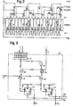
- the time t is used as the abscissa.
- the "1-chirp" signal to be generated is shown in the second line, the "0-chirp” signal as a pulse diagram.
- the alternating 0/1 values of the least significant bit Q 1 of the read-only memory addresses are shown in the third line and the pulses of the first clock signal CL1 are shown in the fifth line.
- Line 4 is a schematic representation of the data values (255 - y j ) or [255 - (y j + 98)] stored in the read-only memory 3 and to be called up at the moment of the positive edge of the first clock signal CL1.
- the diagram is based on an interleaved addressing of the two "chirp" signals. All address fields in line 4 that are below a 0 value of Q 1 therefore belong to "0-Chirp" signal, and the remaining address fields located under a 1 value of Q1 to the "1-Chirp" signal. It should be noted that y j always represents the number of periods T 2 up to the middle of an address field.
- FIG. 2 shows the different possible relative positions of the changes in the value of the two "chirp" signals in relation to the associated address fields and the data values (255 - y.) Or [255 - (y. + 98) J to be stored.
- the last negative going edge of the "O-Chirp" signal occurs at a moment when the data value (255 - y 8 ) of the "1-Chirp" signal is being evaluated (calculated from field center to field center) or, more generally, where A data value of the "1-chirp” signal could have been evaluated, since a non-evaluated data value 255 of the "1-chirp” signal could also have been stored there.
- the data value y 9 belonging to the edge of the "0-chirp” signal must therefore be saved one address field earlier, and not as a value (255 - y 9 ) but as a value [255 - ( y 9 + 98)]
- the output of the "nand” gate 13 feeds a first input of the first "and” gate 16 and via the third inverter 20 a first input of the third "nor” gate 19.
- the respective second inputs of the first "And” gate 16 and the third “Nor” gate 19 are connected to one another and to a single-pole data input D of the logic circuit 12.
- the output of the first "And” gate 16 is at a first input of the second "And” gate 17 and the output of the third "Nor” gate 19 is at a first input of the third "And” gate 18.
- the second Inputs of the second and third “And” gates 17 and 18 are connected to one another and to a clock input T of the logic circuit 12.
- the output of the second "and” gate 17 controls the clock input of the first enable flip-flop 14 and that of the third “and” gate 18 controls that of the second enable flip-flop 15.
- the D and set inputs P of both enable flip-flops Flop 14 and 15 are all logically "1".
- the Q output of the first enable flip-flop 14 is connected to the first output A 1 and that of the second enable flip-flop 15 to the second output B 1 of the logic circuit 12.
- the first reset input R 1 of the logic circuit 12 is at the reset input C of the first enable flip-flop 14 and its second reset input R 2 is at the reset input C of the second enable flip-flop 15.
- the N-bit data values x i are at the N-bit input of the logic circuit and the least significant bit Q 1 of the address of the read-only memory 3 belonging to the data values is at its data input D.
- the respective release flip-flop 14 or 15 is reset at the end of the evaluation if a logical "1" appears at the output of the associated period counter 4 or 5, via the first "Nor” gate 8 of FIGS. 1 and the first reset input R 1 or via the second “Nor” gate 9 of FIG. 1 and the second reset input R 2 . If the evaluation of the relevant period counter 4 or 5 is not released, then a logical "0" is pending at its release input, which enables the loading of the period counter.
Landscapes
- Physics & Mathematics (AREA)
- Nonlinear Science (AREA)
- Oscillators With Electromechanical Resonators (AREA)
- Measurement Of Unknown Time Intervals (AREA)
- Manipulation Of Pulses (AREA)
- Use Of Switch Circuits For Exchanges And Methods Of Control Of Multiplex Exchanges (AREA)
Priority Applications (1)
| Application Number | Priority Date | Filing Date | Title |
|---|---|---|---|
| AT82100055T ATE14959T1 (de) | 1981-05-07 | 1982-01-07 | Verfahren zur erzeugung von digitalen periodischen zeitfunktionssignalen. |
Applications Claiming Priority (2)
| Application Number | Priority Date | Filing Date | Title |
|---|---|---|---|
| CH296081 | 1981-05-07 | ||
| CH2960/81 | 1981-05-07 |
Publications (3)
| Publication Number | Publication Date |
|---|---|
| EP0065062A2 true EP0065062A2 (fr) | 1982-11-24 |
| EP0065062A3 EP0065062A3 (en) | 1983-02-23 |
| EP0065062B1 EP0065062B1 (fr) | 1985-08-14 |
Family
ID=4245505
Family Applications (1)
| Application Number | Title | Priority Date | Filing Date |
|---|---|---|---|
| EP82100055A Expired EP0065062B1 (fr) | 1981-05-07 | 1982-01-07 | Procédé pour la génération de signaux numériques périodiques de fonction de temps |
Country Status (3)
| Country | Link |
|---|---|
| EP (1) | EP0065062B1 (fr) |
| AT (1) | ATE14959T1 (fr) |
| DE (1) | DE3265307D1 (fr) |
Cited By (1)
| Publication number | Priority date | Publication date | Assignee | Title |
|---|---|---|---|---|
| GB2160728A (en) * | 1984-06-21 | 1985-12-24 | Motorola Israel Ltd | Waveform synthesizer |
Family Cites Families (2)
| Publication number | Priority date | Publication date | Assignee | Title |
|---|---|---|---|---|
| US3937899A (en) * | 1975-01-30 | 1976-02-10 | Bell Telephone Laboratories, Incorporated | Tone detector using spectrum parameter estimation |
| US4254327A (en) * | 1979-05-17 | 1981-03-03 | The United States Of America As Represented By The Secretary Of The Navy | Pulse generator having selectable pulse width and pulse repetition interval |
-
1982
- 1982-01-07 AT AT82100055T patent/ATE14959T1/de active
- 1982-01-07 EP EP82100055A patent/EP0065062B1/fr not_active Expired
- 1982-01-07 DE DE8282100055T patent/DE3265307D1/de not_active Expired
Cited By (1)
| Publication number | Priority date | Publication date | Assignee | Title |
|---|---|---|---|---|
| GB2160728A (en) * | 1984-06-21 | 1985-12-24 | Motorola Israel Ltd | Waveform synthesizer |
Also Published As
| Publication number | Publication date |
|---|---|
| EP0065062A3 (en) | 1983-02-23 |
| DE3265307D1 (en) | 1985-09-19 |
| EP0065062B1 (fr) | 1985-08-14 |
| ATE14959T1 (de) | 1985-08-15 |
Similar Documents
| Publication | Publication Date | Title |
|---|---|---|
| EP0084592B1 (fr) | Procédé et dispositif pour mesurer l'intevalle de temps entre les instants d'échantillonnage de deux signaux échantillonnés, en particulier des signaux d'entrée et de sortie d'un convertisseur de fréquence d'échantillonnage | |
| DE2726277C2 (de) | Verfahren zum Ermitteln eines Signals vorgegebener Frequenz und Anordnung zur Durchführung des Verfahrens | |
| DE1951863A1 (de) | Digital betriebener Impulsverhaeltnis-Modulator | |
| DE2537937C2 (de) | Synchronisationsschaltung, die durch Ermittlung eines günstigen Abtastzeitpunktes den Empfang von in einem gestörten Eingangssignal enthaltenen Impulsen ermöglicht | |
| DE1280924B (de) | Bistabile Schaltung | |
| DE2220878B2 (de) | Schaltungsanordnung zur digitalen Frequenzmessung | |
| DE2152687A1 (de) | Verfahren und Einrichtung zum Erkennen einer vorbestimmten Frequenz in einem Frequenzgemisch | |
| DE1591872A1 (de) | Schaltungsanordnung zur Feststellung des Synchronismus zwischen zwei Frequenzen | |
| DE3727941C2 (fr) | ||
| DE2337388C3 (de) | Anordnung zum Gewinnen von periodischen Signalen längerer Dauer und Verfahren zum Betreiben einer solchen Anordnung | |
| DE1437187B2 (de) | Verfahren und Schaltungsanordnung zum Decodieren von binären Impulssignalen | |
| DE1512149C3 (de) | Binäres Verfahren zur Feststellung des Vorzeichens der Phasenverschiebung zwischen periodischen Signalen und Schaltung zur Durchführung des Verfahrens | |
| DE2609563A1 (de) | Generator fuer pseudozufaellige bitfolgen | |
| DE2916976A1 (de) | Speicherschaltung | |
| DE1947555B2 (fr) | ||
| CH616788A5 (fr) | ||
| DE1260530B (de) | Zaehlschaltung zur Zaehlung jedes von einer Vielzahl von angelegten Eingangsimpulsen | |
| DE2704756C2 (de) | Digital-Analog-Umsetzer | |
| EP0065062B1 (fr) | Procédé pour la génération de signaux numériques périodiques de fonction de temps | |
| DE2614794A1 (de) | Verfahren und schaltungsanordnung zum uebertragen binaerer information mittels eines frequenzmodulierten signals | |
| DE2146108A1 (de) | Synchrone Pufferanordnung | |
| EP0243771B1 (fr) | Procédé et dispositif de mesure accélérée et précise de la fréquence d'un signal | |
| DE3843261A1 (de) | Schaltungsanordnung zur steuerung der phase eines taktsignals | |
| DE2002583C2 (de) | Schaltung zum Vorwärts/Rückwärts-Zählen der von einem optischen System gelieferten Interferenzsstreifen | |
| DE2165758A1 (de) | Schaltungsanordnung zur Einstellung der Frequenzteilerschaltung einer elektronischen Uhr |
Legal Events
| Date | Code | Title | Description |
|---|---|---|---|
| PUAI | Public reference made under article 153(3) epc to a published international application that has entered the european phase |
Free format text: ORIGINAL CODE: 0009012 |
|
| AK | Designated contracting states |
Designated state(s): AT BE DE FR NL SE |
|
| PUAL | Search report despatched |
Free format text: ORIGINAL CODE: 0009013 |
|
| AK | Designated contracting states |
Designated state(s): AT BE DE FR NL SE |
|
| 17P | Request for examination filed |
Effective date: 19830316 |
|
| GRAA | (expected) grant |
Free format text: ORIGINAL CODE: 0009210 |
|
| AK | Designated contracting states |
Designated state(s): AT BE DE FR NL SE |
|
| PG25 | Lapsed in a contracting state [announced via postgrant information from national office to epo] |
Ref country code: NL Effective date: 19850814 |
|
| REF | Corresponds to: |
Ref document number: 14959 Country of ref document: AT Date of ref document: 19850815 Kind code of ref document: T |
|
| REF | Corresponds to: |
Ref document number: 3265307 Country of ref document: DE Date of ref document: 19850919 |
|
| ET | Fr: translation filed | ||
| PG25 | Lapsed in a contracting state [announced via postgrant information from national office to epo] |
Ref country code: AT Effective date: 19860107 |
|
| PG25 | Lapsed in a contracting state [announced via postgrant information from national office to epo] |
Ref country code: SE Effective date: 19860108 |
|
| NLV1 | Nl: lapsed or annulled due to failure to fulfill the requirements of art. 29p and 29m of the patents act | ||
| PG25 | Lapsed in a contracting state [announced via postgrant information from national office to epo] |
Ref country code: BE Effective date: 19860131 |
|
| PLBE | No opposition filed within time limit |
Free format text: ORIGINAL CODE: 0009261 |
|
| STAA | Information on the status of an ep patent application or granted ep patent |
Free format text: STATUS: NO OPPOSITION FILED WITHIN TIME LIMIT |
|
| BERE | Be: lapsed |
Owner name: LGZ LANDIS & GYR ZUG A.G. Effective date: 19860131 |
|
| 26N | No opposition filed | ||
| PG25 | Lapsed in a contracting state [announced via postgrant information from national office to epo] |
Ref country code: FR Free format text: LAPSE BECAUSE OF NON-PAYMENT OF DUE FEES Effective date: 19860930 |
|
| PG25 | Lapsed in a contracting state [announced via postgrant information from national office to epo] |
Ref country code: DE Effective date: 19861001 |
|
| REG | Reference to a national code |
Ref country code: FR Ref legal event code: ST |
|
| EUG | Se: european patent has lapsed |
Ref document number: 82100055.1 Effective date: 19861029 |