EP0065115B1 - Justiereinrichtung für Röntgen- oder optische Lithografie - Google Patents
Justiereinrichtung für Röntgen- oder optische Lithografie Download PDFInfo
- Publication number
- EP0065115B1 EP0065115B1 EP82103338A EP82103338A EP0065115B1 EP 0065115 B1 EP0065115 B1 EP 0065115B1 EP 82103338 A EP82103338 A EP 82103338A EP 82103338 A EP82103338 A EP 82103338A EP 0065115 B1 EP0065115 B1 EP 0065115B1
- Authority
- EP
- European Patent Office
- Prior art keywords
- alignment
- wafer
- light
- misalignment
- grating
- Prior art date
- Legal status (The legal status is an assumption and is not a legal conclusion. Google has not performed a legal analysis and makes no representation as to the accuracy of the status listed.)
- Expired
Links
Images





Classifications
-
- G—PHYSICS
- G03—PHOTOGRAPHY; CINEMATOGRAPHY; ANALOGOUS TECHNIQUES USING WAVES OTHER THAN OPTICAL WAVES; ELECTROGRAPHY; HOLOGRAPHY
- G03F—PHOTOMECHANICAL PRODUCTION OF TEXTURED OR PATTERNED SURFACES, e.g. FOR PRINTING, FOR PROCESSING OF SEMICONDUCTOR DEVICES; MATERIALS THEREFOR; ORIGINALS THEREFOR; APPARATUS SPECIALLY ADAPTED THEREFOR
- G03F9/00—Registration or positioning of originals, masks, frames, photographic sheets or textured or patterned surfaces, e.g. automatically
- G03F9/70—Registration or positioning of originals, masks, frames, photographic sheets or textured or patterned surfaces, e.g. automatically for microlithography
- G03F9/7073—Alignment marks and their environment
- G03F9/7076—Mark details, e.g. phase grating mark, temporary mark
-
- G—PHYSICS
- G02—OPTICS
- G02B—OPTICAL ELEMENTS, SYSTEMS OR APPARATUS
- G02B5/00—Optical elements other than lenses
- G02B5/18—Diffraction gratings
- G02B5/1876—Diffractive Fresnel lenses; Zone plates; Kinoforms
-
- G—PHYSICS
- G03—PHOTOGRAPHY; CINEMATOGRAPHY; ANALOGOUS TECHNIQUES USING WAVES OTHER THAN OPTICAL WAVES; ELECTROGRAPHY; HOLOGRAPHY
- G03F—PHOTOMECHANICAL PRODUCTION OF TEXTURED OR PATTERNED SURFACES, e.g. FOR PRINTING, FOR PROCESSING OF SEMICONDUCTOR DEVICES; MATERIALS THEREFOR; ORIGINALS THEREFOR; APPARATUS SPECIALLY ADAPTED THEREFOR
- G03F9/00—Registration or positioning of originals, masks, frames, photographic sheets or textured or patterned surfaces, e.g. automatically
- G03F9/70—Registration or positioning of originals, masks, frames, photographic sheets or textured or patterned surfaces, e.g. automatically for microlithography
- G03F9/7049—Technique, e.g. interferometric
Definitions
- the invention relates to a method and apparatus for aligning a first object with respect to a second object, which finds particular application in X-ray or optical lithography such as is typically employed in the manufacture of integrated circuits.
- Fay et al proposes a Fresnel zone plate on one of the two elements to be aligned, and a reflective stripe, on the other element.
- Fay et al propose the zone plate on the mask, and the stripe on the wafer.
- the zone plate has the property of focusing incident light, so that, for example, by adjusting the proximity gap (distance between wafer and mask) to be equal to the focal length of the zone plate light incident on the zone plate is focused on the wafer.
- the reflective stripe on the wafer has a reflection coefficient which is larger than its surroundings.
- Fay et al propose making the reflecting stripe actually a grating so as to limit or eliminate the zero order reflection from the zone plate. Because the reflective stripe is essenttially a grating the light reflected from the wafer mark is diffracted into many diffraction orders. A photodetector, which is used to detect reflected light, is located so as to collect the first or any higher diffraction order (practically, the first order is the best) and the detected signal will be completely free of zero order reflection. The first order diffraction signal then will produce a convolution signal with very low background when mask and wafer are relatively displaced.
- Fay et a/ employ a scanning mirror in the optical path between the source of light and the mask-wafer, so that by rotating the mirror the angle of incidence of radiation on the mask is varied which results in displacing the incident radiation on the wafer.
- This enables an error signal to be derived without required relative motion between mask and wafer, which error signal can be used to drive the relative displacement error between mask and wafer to zero.
- Fay et al In the experiment reported by Fay et al the scanning motion of the mirror resulted in motion at the wafer of about ⁇ 1 micron. Fay et al also suggests that the wafer grating (typically 1.5 microns in width) be alternated with a wider grating (10 microns in width) with different grating periods such that two alignment signals are returned in slightly different directions. While Fay et al suggests that the signal from the narrow lines could be used for fine alignment and the larger lines could be used for pre-alignment, it is not at all apparent what the form of the signal from the larger lines would be, or how that could be used in pre-alignment.
- EP-A-0010998 of which the inventors are the authors of the above mentioned Fay et al reference, (and corresponding to not-prior- published US-A-4311389) discloses some improvements, including a grating mark shaped so that when there is misalignment, the grating mark diffracts to the light sensor from only a portion of the length of the line image, the size of the length portion varying as a function of the alignment position.
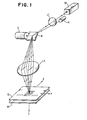
- a light source illustrated as a laser 10 emits a beam of optical energy, which is focussed by lens L1 onto a mirror M which can be rotated by a scanner 11.
- Lens L2 is arranged so that light from a point on the mirror M is image on the mask 12.
- the angle of the mirror M By varying the angle of the mirror M, the angle of incidence of the light beam on the mask 12 can be varied.
- the light incident from lens L2 on the mask 12 is incident on a Fresnel zone plate with focal length equal to the distance (f) between the mask and wafer.
- the light incident on the Fresnel zone plate, of mask 12 will be focussed on the wafer 13.
- the location of the focussed line image on the wafer 13 can be varied. If one measures the angle alpha, between a normal to the mask 12 and the angle of incidence of the light beam, then the displacement in the wafer plane is approximately f tan alpha.
- the returned signal, that is the light reflected by the grating mark on the wafer 13 is shifted laterally due to diffraction, collected by the lens L2 and emerges as a shifted parallel beam beyond lens L1, where suitably placed photo diode 14 is located. Phase locked detection techniques can then be used to generate an error signal with high S/N ratio.
- Fig. 1 is taken from the Fay et al report and his arrangement of a light source, lenses, mirror, and photodiode can be employed in our invention.
- Fig. 2A shows a particular alignment mark on the wafer, consisting of a grating formed by an conventional technique, such as etching, consisting of, in a plan view, a first generally longitudinal grating extending from X1 to X2, and a second generally triangular gating extending from X2 to X3.
- a Fresnel zone plate, located on a mask, for use in conjunction with a wafer alignment mark as shown in Fig. 2A may consist of a linear zone plate which forms a focussed line image shown in dotted outline, for example, at C. More particularly, as illustrated in Fig.
- the line image C between X1 and X4 does not impinge at all on the wafer grating mark whereas the portion of the line image C extending between X3 and X4 does impinge on the wafer grating mark.
- This latter portion of the wafer alignment mark therefore returns a signal via the lenses and mirror to the detecting photo diode. It should be appreciated that, as the distance D between the centerline of the wafer alignment mark and the centerline of the line image C is varied, so will the amount of light diffracted by the wafer alignment mark to the detecting photo diode vary.
- Fig. 2A illustrates the active tracking distance over which an alignment system, employing the wafer alignment mark as shown in Fig. 2A can be used, is determined by the extent of the dimension B. It should also be apparent that the dimension B can be varied almost at will, the only price paid for extending the dimension B, is the wafer area consumed by the alignment mark.
- Fig. 2B illustrates the form of the photo diode signal with respect to misalignment D. It will be seen that a misalignment signal of some positive slope, exists over the entire length of the dimension B.
- the length of the dimension B determines the length over which automatic alignment using the wafer alignment mark of Fig. 2A can be obtained.
- the use of the wafer alignment shown in Fig. 2A eliminates the necessity of rocking the mirror M in order to generate an error signal for use by an automatic alignment apparatus. That is, once the line image C impinges on the wafer alignment mark some recognizable signal is produced by the photo diode 14, and by merely monitoring whether or not that signal is increasing or decreasing, the appropriate direction of slewing is determined for achieving alignment.
- Fig. 2C illustrates the derivative of the curve of Fig. 2B with respect to misalignment distance D which represents a phose detected error signal. This illustrates that the polarity of the detector output, when the incident beam is rocked, determines the appropriate slewing direction to achieve alignment.
- Fig. 3A shows another wafer alignment mark which in many respects is similar to the alignment mark shown in Fig. 2A. That is, more particularly, the wafer alignment mark comprises a grating including a plurality of edges, a first plurality of edges which are generally parallel to one another, and second and third pluralities of edges which each lie on generally converging curves.
- the wafer alignment mark shown in Fig. 3A has generally converging curves which are non-linear, and more particularly have a slope which is generally proportional to misalignment distance.
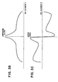
- Use of the alignment mark shown in plan view, in Fig. 3A results in a photo diode detector output varying with misalignment distance D as shown in Fig. 3B.
- Fig. 3C which again represents a phase detected error signal.
- Use of the wafer alignment pattern shown in Fig. 3A has encoded misalignment distance in the waveform of Fig. 3C; this is advantageous in that now the error signal can be used to control the slewing speed of the servo system, so that the servo system can slew rapidly through areas of relatively large misalignment, automatically slowing for fine alignment.
- Fig. 3E shows another wafer alignment mark and the photo diode output takes on the form of Fig. 3D.
- the mark of Fig. 3A has a concave curve (in outline)
- the mark of Fig. 3E is convex.
- the quadratic relation between mark outline and misalignment distance results in a servo circuit (driven by the photo diode) error signal as shown in Fig. 3F.
- the error signal shown in Fig. 3F is linear with misalignment; accordingly, not only is the slewing direction information included in a servo circuit error voltage but distance to alignment is also presented.
- the error voltage of Fig. 3F is again a phase detected signal.
- Figs. 2A and 3A illustrate an example of wafer alignment patterns for generating error signals or derivatives thereof which represent misalignment or distance from alignment.
- Figs. 4A through 4D comprise plan views of other wafer alignment marks.
- Fig. 4A shows a plan view of a wafer alignment mark which, in many respects, is similar to the alignment mark shown in Fig. 2A.
- Fig. 4A shows a plan view of a wafer alignment mark which, in many respects, is similar to the alignment mark shown in Fig. 2A.
- Fig. 4A shows a plan view of a wafer alignment mark which, in many respects, is similar to the alignment mark shown in Fig. 2A.
- Fig. 4A shows a plan view of a wafer alignment mark which, in many respects, is similar to the alignment mark shown in Fig. 2A.
- Fig. 4A shows a plan view of a wafer alignment mark which, in many respects, is similar to the alignment mark shown in Fig
- the grating pattern shown in plan view in Fig. 4A generates one or two pulses, in the photo diode signal, indicative of degree of misalignment.
- the coding scheme used for the alignment mark shown in plan view in Fig. 4A generates a single pulse to indicate a region of relatively large misalignment, and generates a pair of pulses to indicate a region of smaller misalignment.
- the pulse-like output of the photo diode can be isolated and analyzed to determine quantum of misalignment.
- the information derived therefrom can be used to automatically control the slewing speed of a servo motor or other transducer. For example, in such a system as soon as a response from the photo diode is detected, relatively slow slewing is implemented.
- the appropriate direction of slewing can be readily determined from the derivative of the photo diode output, i.e., the absolute value of the derivative should be increasing to indicate slewing toward alignment. This slow slewing is continued until one of the digital signals is encountered. If a two pulse-like signal is encountered, slow slewing is continued, since that information represents a region of relatively small misalignment.
- the slewing speed can be increased, and maintained at a relatively high speed until the two pulse-like signal is encountered, which then generates a change back to the slow slewing speed.
- the coding scheme shown in Fig. 4A. is not at all essential to the invention and, the digital encoding can directly represent degree of misalignment. That is, in this alternative, relatively large misalignment is represented by a pair of pulse-like signals, and a single pulse-like signal represents smaller misalignment.
- more than two different digital signals can be employed depending upon various factors including slewing speed and the extent of the region of automatic alignment, that is the length of the parameter B.
- Fig. 4B illustrates still another wafer alignment pattern which includes the feature of digital encoding, but in a slightly different fashion.
- the wafer alignment pattern which in many respects is similar to that shown in Fig. 2A, has portions (i.e, discontinuities) of the grating removed in direction perpendicular to the longitudinal extent of the light image C.
- the photo diode signal also includes pulse type encoding, but rather than superposing pulse signals on the analog signal as is the case with the alignment mark of Fig. 4A, in the case of the alignment mark shown in Fig. 4B, the analog signal intermittently drops out, each dropout representing a single pulse.
- the alignment marks of Figs. 4A and 4B illustrate digital encoding using the same code but representing that code in the electrical signal, in a different fashion.
- the alignment mark of Fig. 4A places a pulse on the analog signal
- the alignment mark of Fig. 4B results in a dropout of the analog signal corresponding to each pulse.
- the same or similar electronic circuitry or microprocessor or other random logic technology can be employed to detect the presence of the pulses generated by the alignment mark of Fig. 4B, for similar purposes.
- the digital encoding and the alignment marks of Figs. 4A and 4B have been used in a single alignment mark to generate in the photo diode, a composite signal comprising the superposition of an analog and digital signal. That is not at all essential to the invention and, rather an alignment mark shown in Fig. 4C can be used to generate only digital signals. Since the alignment mark of Fig. 4C provides information to the photo diode only when the light image C crosses one of the alignment marks no information is provided to an automatic alignment system when the light image C is in a region between or outside of the alignment mark. For this reason, preferably the alignment mark whose plan view is shown in Fig. 4C is used in conjunction with an alignment mark as shown, for example, in Figs.
- the wafer includes two alignment marks, one digitally encoded and the other encoded in analog fashion, and cooperating with each alignment mark is a different Fresnel zone plate for focussing incident illumination thereon or a single broad zone plate for imaging both marks.
- the alignment mark comprises a plurality of gratings, taken in groups, and the number of gratings in each group provides information as to misalignment.
- a single grating indicates relatively large misalignment
- a pair of gratings indicates relatively less misalignment
- three gratings in a group indicates a minimum misalignment.
- Fig. 4D uses the same type of coding as is shown in Fig. 4C; however, rather than using one, two, three or more gratings per groups to produce one, two, three or more pulses representing misalignment, the alignment pattern shown in Fig. 4D normally produces a relatively high signal from the photo diode, and that signal drops out to generate the pulse-like signals indicative of misalignment.
- Fresnel zone plates and wafer alignment marks whose width (that is a dimension generally perpendicular to the longitudinal extent of a light image C) is substantial, especially when considered in relation to the desired alignment accuracy of ⁇ 0.05 microns.
- Fay et al indicates that in order to increase the signal level the alignment mark used in their experimental investigation comprised a matrix of individual Fresnel zone plates covering the area of 1 square millimeter, and the corresponding wafer alignment mark is also a matrix of gratings (presumably also approximately 1 square millimeter in extent).
- a periodic mask zone plate results in a measuring ambiguity at a distance equal to the period. For example, a periodic zone plate with period of 100 microns will produce exactly identical signals at proper alignment and when misalignment is 100 microns.
- each "element” is a Fresnel zone plate with focal length nominally equal to desired mask-wafer separation distance (for example, on the order of several microns). This ensures that radiation incident on the mask zone plate is focused on the wafer.
- each "element” is located to form a larger or macro Fresnel zone plate which has a different focal length. Referring briefly to Fig. 1 it will be seen that whereas the separation distance between mask 12 and wafer 13 is relatively small, the optical distance between mask 12 and photo diode 14 is much larger (measured, for example, in centimeters).
- Fig. 5A shows the macro Fresnel lines as comprising a series of elements "E" at about 40x actual size, which was 4 mm 2 . In Fig. 5A dark regions are opaque.
- each element E of Fig. 5A is shown, in detail in Fig. 5B, magnified 1600x.
- the spacing and width of each elemental transparent zone T is adjusted to focus the incident radiation in a distance nominally equal to mask-wafer separation.
- the elements "E” result in a different focal length (in one example 10 cm) selected to match mask to photo diode optical distance.
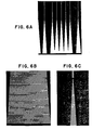
- Figs. 6A-6C illustrate a wafer alignment mark comprising plural marks each of a shape in accordance with Fig. 2A.
- Fig. 6A shows the alignment mark (magnification 80)
- Fig. 6B shows the base of one element (magnification 800)
- Fig. 6C shows the apex and its intersection with the rectangular grating (magnification 1000).
- Fig. 6A illustrates that the quantum of useable diffracted light has been multiplied by covering a large area with repeats of an elemental wafer grating pattern.
- Figs. 7A and 7B illustrate the advantage of the aperiodic macro Fresnel zone plate in eliminating alignment ambiguity.
- Fig. 7B is a trace of expected detector signal vs. misalignment for a prior art periodic Fresnel zone plate of 100 micron period. Note the alignment ambiguity of ⁇ 50 microns.
- Fig. 7A is a photo diode signal vs. misalignment ( ⁇ 200 microns) with a macro Fresnel zone plate. Clearly, misalignment ambiguity has been eliminated.
Landscapes
- Physics & Mathematics (AREA)
- General Physics & Mathematics (AREA)
- Optics & Photonics (AREA)
- Exposure And Positioning Against Photoresist Photosensitive Materials (AREA)
- Exposure Of Semiconductors, Excluding Electron Or Ion Beam Exposure (AREA)
- Length Measuring Devices By Optical Means (AREA)
- Control Of Position Or Direction (AREA)
Claims (5)
Applications Claiming Priority (2)
| Application Number | Priority Date | Filing Date | Title |
|---|---|---|---|
| US06/265,140 US4405238A (en) | 1981-05-20 | 1981-05-20 | Alignment method and apparatus for x-ray or optical lithography |
| US265140 | 1981-05-20 |
Publications (2)
| Publication Number | Publication Date |
|---|---|
| EP0065115A1 EP0065115A1 (de) | 1982-11-24 |
| EP0065115B1 true EP0065115B1 (de) | 1985-08-07 |
Family
ID=23009187
Family Applications (1)
| Application Number | Title | Priority Date | Filing Date |
|---|---|---|---|
| EP82103338A Expired EP0065115B1 (de) | 1981-05-20 | 1982-04-21 | Justiereinrichtung für Röntgen- oder optische Lithografie |
Country Status (4)
| Country | Link |
|---|---|
| US (1) | US4405238A (de) |
| EP (1) | EP0065115B1 (de) |
| JP (1) | JPS57191502A (de) |
| DE (1) | DE3265191D1 (de) |
Families Citing this family (30)
| Publication number | Priority date | Publication date | Assignee | Title |
|---|---|---|---|---|
| US4765714A (en) * | 1984-04-03 | 1988-08-23 | Horner Joseph L | Binary phase-only optical correlation system |
| JPH0726803B2 (ja) * | 1984-11-26 | 1995-03-29 | 株式会社ニコン | 位置検出方法及び装置 |
| DE3704313A1 (de) * | 1986-11-20 | 1988-06-01 | Krupp Gmbh | Beruehrungsloses optisches verfahren zur bestimmung von gegenstaenden |
| US4815854A (en) * | 1987-01-19 | 1989-03-28 | Nec Corporation | Method of alignment between mask and semiconductor wafer |
| US4791482A (en) * | 1987-02-06 | 1988-12-13 | Westinghouse Electric Corp. | Object locating system |
| JPH01285803A (ja) * | 1988-05-13 | 1989-11-16 | Fujitsu Ltd | フレネル・ゾーン・プレートおよびそれを用いる位置合せ方法 |
| JPH07119574B2 (ja) * | 1988-09-12 | 1995-12-20 | 富士通株式会社 | 二次元位置検出方法 |
| JP2666859B2 (ja) * | 1988-11-25 | 1997-10-22 | 日本電気株式会社 | 目合せ用バーニヤパターンを備えた半導体装置 |
| JP2925168B2 (ja) * | 1989-07-28 | 1999-07-28 | キヤノン株式会社 | 位置検出装置及び方法 |
| US5229617A (en) * | 1989-07-28 | 1993-07-20 | Canon Kabushiki Kaisha | Position detecting method having reflectively scattered light prevented from impinging on a detector |
| JP3008633B2 (ja) * | 1991-01-11 | 2000-02-14 | キヤノン株式会社 | 位置検出装置 |
| JP2592369B2 (ja) * | 1991-08-22 | 1997-03-19 | 富士通株式会社 | 多層配線回路基板の製造方法及び誘電体ミラーマスクの製造方法 |
| US5504596A (en) * | 1992-12-21 | 1996-04-02 | Nikon Corporation | Exposure method and apparatus using holographic techniques |
| US5864394A (en) * | 1994-06-20 | 1999-01-26 | Kla-Tencor Corporation | Surface inspection system |
| US5576831A (en) * | 1994-06-20 | 1996-11-19 | Tencor Instruments | Wafer alignment sensor |
| US5883710A (en) | 1994-12-08 | 1999-03-16 | Kla-Tencor Corporation | Scanning system for inspecting anomalies on surfaces |
| US20040057044A1 (en) * | 1994-12-08 | 2004-03-25 | Mehrdad Nikoonahad | Scanning system for inspecting anamolies on surfaces |
| US5825482A (en) * | 1995-09-29 | 1998-10-20 | Kla-Tencor Corporation | Surface inspection system with misregistration error correction and adaptive illumination |
| DE19609399C2 (de) * | 1996-03-01 | 2002-05-29 | Infineon Technologies Ag | Verfahren zum Bestimmen der Kristallorientierung in einem Wafer |
| JP4306800B2 (ja) * | 1996-06-04 | 2009-08-05 | ケーエルエー−テンカー テクノロジィース コーポレイション | 表面検査用光学走査システム |
| US5973316A (en) * | 1997-07-08 | 1999-10-26 | Nec Research Institute, Inc. | Sub-wavelength aperture arrays with enhanced light transmission |
| US6040936A (en) * | 1998-10-08 | 2000-03-21 | Nec Research Institute, Inc. | Optical transmission control apparatus utilizing metal films perforated with subwavelength-diameter holes |
| US6236033B1 (en) | 1998-12-09 | 2001-05-22 | Nec Research Institute, Inc. | Enhanced optical transmission apparatus utilizing metal films having apertures and periodic surface topography |
| US6285020B1 (en) | 1999-11-05 | 2001-09-04 | Nec Research Institute, Inc. | Enhanced optical transmission apparatus with improved inter-surface coupling |
| US6441298B1 (en) | 2000-08-15 | 2002-08-27 | Nec Research Institute, Inc | Surface-plasmon enhanced photovoltaic device |
| US6552809B1 (en) | 2000-09-18 | 2003-04-22 | Institut National D'optique | Position encoding optical device and method |
| US6649901B2 (en) | 2002-03-14 | 2003-11-18 | Nec Laboratories America, Inc. | Enhanced optical transmission apparatus with improved aperture geometry |
| US8225664B1 (en) * | 2007-10-17 | 2012-07-24 | Lsp Technologies | Lamb waves for laser bond inspection |
| CN101694531B (zh) * | 2009-10-15 | 2011-01-05 | 电子科技大学 | 过剩光载流子菲涅耳波带片 |
| KR102695015B1 (ko) * | 2018-09-17 | 2024-08-13 | 삼성전자주식회사 | 네가티브톤 현상용 포토마스크 |
Family Cites Families (6)
| Publication number | Priority date | Publication date | Assignee | Title |
|---|---|---|---|---|
| US3545854A (en) * | 1966-06-17 | 1970-12-08 | Gen Electric | Semiconductor mask making |
| JPS4842764A (de) * | 1971-09-29 | 1973-06-21 | ||
| US4037969A (en) * | 1976-04-02 | 1977-07-26 | Bell Telephone Laboratories, Incorporated | Zone plate alignment marks |
| FR2436967A1 (fr) * | 1978-09-19 | 1980-04-18 | Thomson Csf | Procede d'alignement optique de motifs dans deux plans rapproches et dispositif d'alignement mettant en oeuvre un tel procede |
| US4360586A (en) * | 1979-05-29 | 1982-11-23 | Massachusetts Institute Of Technology | Spatial period division exposing |
| US4326805A (en) * | 1980-04-11 | 1982-04-27 | Bell Telephone Laboratories, Incorporated | Method and apparatus for aligning mask and wafer members |
-
1981
- 1981-05-20 US US06/265,140 patent/US4405238A/en not_active Expired - Lifetime
-
1982
- 1982-03-18 JP JP57041832A patent/JPS57191502A/ja active Granted
- 1982-04-21 DE DE8282103338T patent/DE3265191D1/de not_active Expired
- 1982-04-21 EP EP82103338A patent/EP0065115B1/de not_active Expired
Also Published As
| Publication number | Publication date |
|---|---|
| EP0065115A1 (de) | 1982-11-24 |
| JPS57191502A (en) | 1982-11-25 |
| US4405238A (en) | 1983-09-20 |
| DE3265191D1 (en) | 1985-09-12 |
| JPS6312522B2 (de) | 1988-03-19 |
Similar Documents
| Publication | Publication Date | Title |
|---|---|---|
| EP0065115B1 (de) | Justiereinrichtung für Röntgen- oder optische Lithografie | |
| US4677293A (en) | Photoelectric measuring system | |
| KR100363034B1 (ko) | 격자-격자간섭계정렬장치 | |
| DE69632564T2 (de) | Verschiebungsinformationserfassungsvorrichtung | |
| US6552809B1 (en) | Position encoding optical device and method | |
| DE69320716T3 (de) | Gerät zur Detektion von Verschiebungsinformation | |
| US4566795A (en) | Alignment apparatus | |
| KR930000878B1 (ko) | 리니어 프레스넬 존 플레이트(Linear Fresnel Zone Plate)를 사용한 마스크와 반도체웨이퍼의 위치맞춤시스템 및 방법 | |
| EP0220757B1 (de) | Optisches Messgrössenumformerelement und Verschiebungsmessvorrichtung mit einem solchen Element | |
| PL86214B1 (de) | ||
| Fay et al. | Optical alignment system for submicron x‐ray lithography | |
| EP0871072B1 (de) | Detektor mit mehreren Öffnungen für die Photolithographie | |
| CN112585431A (zh) | 线性和旋转多轨道绝对位置编码器及其使用方法 | |
| US4579453A (en) | Method and apparatus for detecting a mark position | |
| US5285259A (en) | Position detecting method | |
| US5539446A (en) | Light beam position detection and control apparatus employing diffraction patterns | |
| US4663534A (en) | Position detecting device utilizing selective outputs of the photodetector for accurate alignment | |
| US5322999A (en) | Method and apparatus for precision control of galvanometer patterning system | |
| JP2750618B2 (ja) | 光学式変位検出装置 | |
| JP3191417B2 (ja) | エンコーダ装置 | |
| JP2822225B2 (ja) | 光学式変位検出装置 | |
| US4808807A (en) | Optical focus sensor system | |
| JP2513281B2 (ja) | 位置合わせ装置 | |
| JPS61116837A (ja) | 回折格子によるギヤツプ・位置合せ制御法 | |
| JPH0429962B2 (de) |
Legal Events
| Date | Code | Title | Description |
|---|---|---|---|
| PUAI | Public reference made under article 153(3) epc to a published international application that has entered the european phase |
Free format text: ORIGINAL CODE: 0009012 |
|
| AK | Designated contracting states |
Designated state(s): DE FR GB IT |
|
| 17P | Request for examination filed |
Effective date: 19830322 |
|
| GRAA | (expected) grant |
Free format text: ORIGINAL CODE: 0009210 |
|
| AK | Designated contracting states |
Designated state(s): DE FR GB IT |
|
| PG25 | Lapsed in a contracting state [announced via postgrant information from national office to epo] |
Ref country code: IT Free format text: LAPSE BECAUSE OF FAILURE TO SUBMIT A TRANSLATION OF THE DESCRIPTION OR TO PAY THE FEE WITHIN THE PRESCRIBED TIME-LIMIT;WARNING: LAPSES OF ITALIAN PATENTS WITH EFFECTIVE DATE BEFORE 2007 MAY HAVE OCCURRED AT ANY TIME BEFORE 2007. THE CORRECT EFFECTIVE DATE MAY BE DIFFERENT FROM THE ONE RECORDED. Effective date: 19850807 |
|
| REF | Corresponds to: |
Ref document number: 3265191 Country of ref document: DE Date of ref document: 19850912 |
|
| ET | Fr: translation filed | ||
| PLBE | No opposition filed within time limit |
Free format text: ORIGINAL CODE: 0009261 |
|
| STAA | Information on the status of an ep patent application or granted ep patent |
Free format text: STATUS: NO OPPOSITION FILED WITHIN TIME LIMIT |
|
| 26N | No opposition filed | ||
| PGFP | Annual fee paid to national office [announced via postgrant information from national office to epo] |
Ref country code: FR Payment date: 19920226 Year of fee payment: 11 |
|
| PGFP | Annual fee paid to national office [announced via postgrant information from national office to epo] |
Ref country code: GB Payment date: 19920304 Year of fee payment: 11 |
|
| PGFP | Annual fee paid to national office [announced via postgrant information from national office to epo] |
Ref country code: DE Payment date: 19920504 Year of fee payment: 11 |
|
| PG25 | Lapsed in a contracting state [announced via postgrant information from national office to epo] |
Ref country code: GB Effective date: 19930421 |
|
| GBPC | Gb: european patent ceased through non-payment of renewal fee |
Effective date: 19930421 |
|
| PG25 | Lapsed in a contracting state [announced via postgrant information from national office to epo] |
Ref country code: FR Effective date: 19931229 |
|
| PG25 | Lapsed in a contracting state [announced via postgrant information from national office to epo] |
Ref country code: DE Effective date: 19940101 |
|
| REG | Reference to a national code |
Ref country code: FR Ref legal event code: ST |