EP0065133A2 - Diode à barrière Schottky à anneau de garde et procédé de fabrication - Google Patents
Diode à barrière Schottky à anneau de garde et procédé de fabrication Download PDFInfo
- Publication number
- EP0065133A2 EP0065133A2 EP82103562A EP82103562A EP0065133A2 EP 0065133 A2 EP0065133 A2 EP 0065133A2 EP 82103562 A EP82103562 A EP 82103562A EP 82103562 A EP82103562 A EP 82103562A EP 0065133 A2 EP0065133 A2 EP 0065133A2
- Authority
- EP
- European Patent Office
- Prior art keywords
- layer
- substrate
- dielectric layer
- hole
- silicon
- Prior art date
- Legal status (The legal status is an assumption and is not a legal conclusion. Google has not performed a legal analysis and makes no representation as to the accuracy of the status listed.)
- Granted
Links
- 230000004888 barrier function Effects 0.000 title claims abstract description 16
- 238000004519 manufacturing process Methods 0.000 title description 3
- XUIMIQQOPSSXEZ-UHFFFAOYSA-N Silicon Chemical compound [Si] XUIMIQQOPSSXEZ-UHFFFAOYSA-N 0.000 claims abstract description 22
- 229910052710 silicon Inorganic materials 0.000 claims abstract description 21
- 239000010703 silicon Substances 0.000 claims abstract description 21
- 239000000758 substrate Substances 0.000 claims abstract description 21
- 239000002184 metal Substances 0.000 claims abstract description 11
- 229910052751 metal Inorganic materials 0.000 claims abstract description 11
- 239000002019 doping agent Substances 0.000 claims abstract description 7
- 238000010438 heat treatment Methods 0.000 claims abstract 2
- 238000000034 method Methods 0.000 claims description 17
- 238000000151 deposition Methods 0.000 claims description 7
- 238000005530 etching Methods 0.000 claims description 4
- 239000003989 dielectric material Substances 0.000 claims description 2
- 238000000992 sputter etching Methods 0.000 claims 2
- VYPSYNLAJGMNEJ-UHFFFAOYSA-N Silicium dioxide Chemical compound O=[Si]=O VYPSYNLAJGMNEJ-UHFFFAOYSA-N 0.000 description 20
- 229910052681 coesite Inorganic materials 0.000 description 12
- 229910052906 cristobalite Inorganic materials 0.000 description 12
- 229910052682 stishovite Inorganic materials 0.000 description 12
- 229910052905 tridymite Inorganic materials 0.000 description 12
- 229910021420 polycrystalline silicon Inorganic materials 0.000 description 10
- 239000000377 silicon dioxide Substances 0.000 description 7
- 229920005591 polysilicon Polymers 0.000 description 5
- 238000001020 plasma etching Methods 0.000 description 4
- 229920002120 photoresistant polymer Polymers 0.000 description 3
- 238000009792 diffusion process Methods 0.000 description 2
- 150000002500 ions Chemical class 0.000 description 2
- 239000002210 silicon-based material Substances 0.000 description 2
- VLJQDHDVZJXNQL-UHFFFAOYSA-N 4-methyl-n-(oxomethylidene)benzenesulfonamide Chemical compound CC1=CC=C(S(=O)(=O)N=C=O)C=C1 VLJQDHDVZJXNQL-UHFFFAOYSA-N 0.000 description 1
- 230000002411 adverse Effects 0.000 description 1
- 229910052782 aluminium Inorganic materials 0.000 description 1
- 238000000137 annealing Methods 0.000 description 1
- 229910052804 chromium Inorganic materials 0.000 description 1
- 230000008021 deposition Effects 0.000 description 1
- 230000000694 effects Effects 0.000 description 1
- 230000005684 electric field Effects 0.000 description 1
- 229910052735 hafnium Inorganic materials 0.000 description 1
- 230000010354 integration Effects 0.000 description 1
- 229910052750 molybdenum Inorganic materials 0.000 description 1
- 150000004767 nitrides Chemical group 0.000 description 1
- 229910052763 palladium Inorganic materials 0.000 description 1
- 238000000206 photolithography Methods 0.000 description 1
- 229910052697 platinum Inorganic materials 0.000 description 1
- 229910021340 platinum monosilicide Inorganic materials 0.000 description 1
- 229910021332 silicide Inorganic materials 0.000 description 1
- FVBUAEGBCNSCDD-UHFFFAOYSA-N silicide(4-) Chemical compound [Si-4] FVBUAEGBCNSCDD-UHFFFAOYSA-N 0.000 description 1
- 235000012239 silicon dioxide Nutrition 0.000 description 1
- 238000003860 storage Methods 0.000 description 1
- 229910052715 tantalum Inorganic materials 0.000 description 1
- 229910052719 titanium Inorganic materials 0.000 description 1
Images

Classifications
-
- H—ELECTRICITY
- H10—SEMICONDUCTOR DEVICES; ELECTRIC SOLID-STATE DEVICES NOT OTHERWISE PROVIDED FOR
- H10D—INORGANIC ELECTRIC SEMICONDUCTOR DEVICES
- H10D8/00—Diodes
- H10D8/60—Schottky-barrier diodes
Definitions
- the invention relates to a Schottky barrier diode with a guard ring comprising a dielectric layer on a silicon substrate said layer having a hole therein and Schottky barrier contact metal contacting said silicon substrate in said hole and within the outer periphery of said guard ring and a method of producing such a diode.
- the area of the guard ring depends upon the extent of lateral undercut of nitride-oxide layers which, in turn, depends upon the etching time of the underlying oxide layer. Neither technique provides optimum area control whereby the smallest area self-aligned guard rings are achieved in a reproducible manner.
- IBMfR Technical Disclosure Bulletin, Vol. 21, No. 7, December 1978, pg. 2752 describes a technique for using a boron-doped polysilicon ring for diffusing the guard ring area of a Schottky diode but the polysilicon ring is determined photolithographically and is not of minimum area.
- the area of the guard ring is reduced to a very accurately controlled minimum. This structure can be achieved, because the guard ring is formed self-aligned with the Schottky contact.
- the thickness of the polycrystalline ring must be sufficient to fill in the undercut region of the oxide, the dimensions of which can not be closely controlled. If the ring, contrary to the teaching of said copending patent application, had been doped so as to form a guard ring, the area of the guard ring would likewise not be closely controllable.
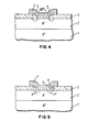
- Figs. 1 - 4 are a series of cross-sectional views of a preferred embodiment of the invention showing the structure resulting at successive times during the course of fabrication;
- Fig. 5 is a cross-sectional view of an alternative embodiment.
- N- epitaxial layer 2 of about 0.3 ⁇ cm silicon material, is deposited to a thickness of about 1 micrometer.
- Epitaxial layer 2 is covered with a dielectric material such as thermally grown silicon dioxide layer 3 to a thickness preferably in the range of about 200 nm to about 500 nm.
- the Si0 2 layer 3 is covered by a photoresist (not shown), for example, approximately 1 nm thickness of HC (high contrast) resist. The photoresist is exposed and developed in those areas where Schottky diode contacts are desired to be located.
- the Si0 2 layer 3 is anisotropically etched, as by reactive ion etching, to produce substantially vertically-walled holes in Si0 2 layer 3 where Schottky diode contacts are desired. Then, as shown in Fig. 2, p+ doped polycrystalline silicon layer 4 is deposited to a thickness preferably in the range from about 250 nm to about 300 nm.
- the thickness of polysilicon layer 4 is closely controlled as it will determine the area of a self-aligned guard ring to be formed in epi layer 2 after further processing.
- the processing includes the reactive ion etching and dopant drive-in techniques disclosed in U.S. patent 4,209,350, issued June 24, 1980 to Ho et al. for Method For Forming Diffusions Having Narrow Dimensions Utilizing Reactive Ion Etching and assigned to the present assignee.
- the reactive ion etching of doped polysilicon layer 4 removes said layer from all horizontal surfaces of the structure of Fig. 2, leaving doped polycrystalline silicon only along the substantially vertical surfaces of the edges of the hole in SiO 2 layer 3 as shown in Fig. 3.
- the resulting structure is annealed at a suitable temperature and time, such as at about 1000°C for about 1 hour, to cause the dopant in polysilicon sidewall 5 to diffuse into epi layer 2 to form guard ring 6.
- the Schottky diode is completed by deposition of suitable metal 7 of Fig. 4 such as-the group comprising PtSi, Pt, Pd, Al and Mo (for high barrier diodes ⁇ . If a low barrier diode is required, a metal such as Ti, Ta, Hf, Cr or Ti-W may be used as the Schottky contact metal.
- the fabrication process initially is the same as described in connection with Fig. 1. After SiO 2 layer 3 is apertured, however, another layer of SiO 2 is chemically vapor deposited and is reactively ion etched to leave only sidewall portion 8 which partially fills in the hole originally etched in SiO 2 layer 3.
- the structure then is completed as described before, i.e., a layer of doped polycrystalline silicon is deposited and reactively ion etched to leave only sidewall portion 5', the dopant is driven into the epi 3' by annealing and an appropriate Schottky contact metal 7' is deposited.
- the minimum thickness or width W of the doped sidewall portion 5 and 5' of Figs. 4 and 5, respectively, should be of the order of about 100 nm so the resultant guard ring is of sufficient area to reduce the electric field at the corners of the Schottky diode contact to acceptable levels.
- the maximum width of the total sidewall portions is limited by the thickness of the SiO 2 layer 3. Therefore, the thickness of the Si0 2 layer 3 in the single sidewall case of Fig. 4 generally should be greater than 100 nm but need not be greater than about 300 nm while the SiO 2 layer 3 thickness in the double sidewall case of Fig. 5 generally need not be greater than about 500 nm.
- the dopant concentration in the doped sidewall portion should be at least one order of magnitude greater than the dopant concentration in the underlying epi layer.
Landscapes
- Electrodes Of Semiconductors (AREA)
Applications Claiming Priority (2)
| Application Number | Priority Date | Filing Date | Title |
|---|---|---|---|
| US06/263,227 US4691435A (en) | 1981-05-13 | 1981-05-13 | Method for making Schottky diode having limited area self-aligned guard ring |
| US263227 | 1981-05-13 |
Publications (3)
| Publication Number | Publication Date |
|---|---|
| EP0065133A2 true EP0065133A2 (fr) | 1982-11-24 |
| EP0065133A3 EP0065133A3 (en) | 1984-12-27 |
| EP0065133B1 EP0065133B1 (fr) | 1988-01-07 |
Family
ID=23000899
Family Applications (1)
| Application Number | Title | Priority Date | Filing Date |
|---|---|---|---|
| EP82103562A Expired EP0065133B1 (fr) | 1981-05-13 | 1982-04-27 | Diode à barrière Schottky à anneau de garde et procédé de fabrication |
Country Status (4)
| Country | Link |
|---|---|
| US (1) | US4691435A (fr) |
| EP (1) | EP0065133B1 (fr) |
| JP (1) | JPS57187970A (fr) |
| DE (1) | DE3277955D1 (fr) |
Cited By (3)
| Publication number | Priority date | Publication date | Assignee | Title |
|---|---|---|---|---|
| EP0182088A1 (fr) * | 1984-10-26 | 1986-05-28 | Siemens Aktiengesellschaft | Contact Schottky à la surface d'un semi-conducteur et son procédé de réalisatioN |
| EP0174686A3 (en) * | 1984-08-30 | 1988-03-16 | Philips Patentverwaltung Gmbh | Semiconductor temperature sensor |
| WO1999062124A1 (fr) * | 1998-05-26 | 1999-12-02 | Siemens Aktiengesellschaft | Procede de production de diodes schottky |
Families Citing this family (21)
| Publication number | Priority date | Publication date | Assignee | Title |
|---|---|---|---|---|
| US4807013A (en) * | 1984-10-17 | 1989-02-21 | American Telephone And Telegraph Company At&T Bell Laboratories | Polysilicon fillet |
| US4939154A (en) * | 1987-03-25 | 1990-07-03 | Seiko Instruments Inc. | Method of fabricating an insulated gate semiconductor device having a self-aligned gate |
| JPH0766968B2 (ja) * | 1987-08-24 | 1995-07-19 | 株式会社日立製作所 | 半導体装置及びその製造方法 |
| US5179034A (en) * | 1987-08-24 | 1993-01-12 | Hitachi, Ltd. | Method for fabricating insulated gate semiconductor device |
| US4898841A (en) * | 1988-06-16 | 1990-02-06 | Northern Telecom Limited | Method of filling contact holes for semiconductor devices and contact structures made by that method |
| US5262339A (en) * | 1989-06-12 | 1993-11-16 | Hitachi, Ltd. | Method of manufacturing a power semiconductor device using implants and solid diffusion source |
| US5270256A (en) * | 1991-11-27 | 1993-12-14 | Intel Corporation | Method of forming a guard wall to reduce delamination effects |
| JP2679647B2 (ja) * | 1994-09-28 | 1997-11-19 | 日本電気株式会社 | 半導体装置 |
| US5696025A (en) * | 1996-02-02 | 1997-12-09 | Micron Technology, Inc. | Method of forming guard ringed schottky diode |
| JP3287269B2 (ja) * | 1997-06-02 | 2002-06-04 | 富士電機株式会社 | ダイオードとその製造方法 |
| SG70654A1 (en) | 1997-09-30 | 2000-02-22 | Ibm | Copper stud structure with refractory metal liner |
| US5859450A (en) * | 1997-09-30 | 1999-01-12 | Intel Corporation | Dark current reducing guard ring |
| US6117719A (en) * | 1997-12-18 | 2000-09-12 | Advanced Micro Devices, Inc. | Oxide spacers as solid sources for gallium dopant introduction |
| JP2003514371A (ja) * | 1998-05-26 | 2003-04-15 | インフィネオン テクノロジース アクチエンゲゼルシャフト | ショットキーダイオードの製法 |
| KR100699747B1 (ko) * | 2000-11-07 | 2007-03-27 | 페어차일드코리아반도체 주식회사 | 쇼트키 다이오드의 제조 방법 |
| US7262434B2 (en) * | 2002-03-28 | 2007-08-28 | Rohm Co., Ltd. | Semiconductor device with a silicon carbide substrate and ohmic metal layer |
| US6902867B2 (en) * | 2002-10-02 | 2005-06-07 | Lexmark International, Inc. | Ink jet printheads and methods therefor |
| DE10330838B4 (de) | 2003-07-08 | 2005-08-25 | Infineon Technologies Ag | Elektronisches Bauelement mit Schutzring |
| US8901699B2 (en) | 2005-05-11 | 2014-12-02 | Cree, Inc. | Silicon carbide junction barrier Schottky diodes with suppressed minority carrier injection |
| US8435873B2 (en) | 2006-06-08 | 2013-05-07 | Texas Instruments Incorporated | Unguarded Schottky barrier diodes with dielectric underetch at silicide interface |
| CN114335154B (zh) * | 2022-03-10 | 2022-07-01 | 深圳市威兆半导体有限公司 | 一种半导体器件、终端结构及其制造方法 |
Family Cites Families (10)
| Publication number | Priority date | Publication date | Assignee | Title |
|---|---|---|---|---|
| US3821772A (en) * | 1971-10-22 | 1974-06-28 | Motorola Inc | Schottky diode with minimal metal guard ring overlap |
| US3907617A (en) * | 1971-10-22 | 1975-09-23 | Motorola Inc | Manufacture of a high voltage Schottky barrier device |
| US4038107B1 (en) * | 1975-12-03 | 1995-04-18 | Samsung Semiconductor Tele | Method for making transistor structures |
| US4063964A (en) * | 1976-12-27 | 1977-12-20 | International Business Machines Corporation | Method for forming a self-aligned schottky barrier device guardring |
| JPS586313B2 (ja) * | 1978-06-13 | 1983-02-03 | 日本電信電話株式会社 | ガ−ドリングを有するシヨツトキダイオ−ド及びその製法 |
| US4209349A (en) * | 1978-11-03 | 1980-06-24 | International Business Machines Corporation | Method for forming a narrow dimensioned mask opening on a silicon body utilizing reactive ion etching |
| US4256514A (en) * | 1978-11-03 | 1981-03-17 | International Business Machines Corporation | Method for forming a narrow dimensioned region on a body |
| US4209350A (en) * | 1978-11-03 | 1980-06-24 | International Business Machines Corporation | Method for forming diffusions having narrow dimensions utilizing reactive ion etching |
| US4356623A (en) * | 1980-09-15 | 1982-11-02 | Texas Instruments Incorporated | Fabrication of submicron semiconductor devices |
| US4414737A (en) * | 1981-01-30 | 1983-11-15 | Tokyo Shibaura Denki Kabushiki Kaisha | Production of Schottky barrier diode |
-
1981
- 1981-05-13 US US06/263,227 patent/US4691435A/en not_active Expired - Fee Related
-
1982
- 1982-01-20 JP JP57006187A patent/JPS57187970A/ja active Pending
- 1982-04-27 DE DE8282103562T patent/DE3277955D1/de not_active Expired
- 1982-04-27 EP EP82103562A patent/EP0065133B1/fr not_active Expired
Cited By (3)
| Publication number | Priority date | Publication date | Assignee | Title |
|---|---|---|---|---|
| EP0174686A3 (en) * | 1984-08-30 | 1988-03-16 | Philips Patentverwaltung Gmbh | Semiconductor temperature sensor |
| EP0182088A1 (fr) * | 1984-10-26 | 1986-05-28 | Siemens Aktiengesellschaft | Contact Schottky à la surface d'un semi-conducteur et son procédé de réalisatioN |
| WO1999062124A1 (fr) * | 1998-05-26 | 1999-12-02 | Siemens Aktiengesellschaft | Procede de production de diodes schottky |
Also Published As
| Publication number | Publication date |
|---|---|
| EP0065133A3 (en) | 1984-12-27 |
| JPS57187970A (en) | 1982-11-18 |
| DE3277955D1 (en) | 1988-02-11 |
| EP0065133B1 (fr) | 1988-01-07 |
| US4691435A (en) | 1987-09-08 |
Similar Documents
| Publication | Publication Date | Title |
|---|---|---|
| EP0065133B1 (fr) | Diode à barrière Schottky à anneau de garde et procédé de fabrication | |
| US5106767A (en) | Process for fabricating low capacitance bipolar junction transistor | |
| JP2744808B2 (ja) | 自己整合トランジスタの製造方法 | |
| US4711017A (en) | Formation of buried diffusion devices | |
| EP0036082A1 (fr) | Procédé autoaligné pour la réalisation d'un transistor bipolaire à haute performance | |
| EP0418185A1 (fr) | Procédé de fabrication d'une transistor avec une base mince | |
| US5187109A (en) | Lateral bipolar transistor and method of making the same | |
| EP0205008B1 (fr) | Structure semi-conductrice intégrée et procédé de fabrication | |
| EP0033495B1 (fr) | Procédé de fabrication d'un transistor bipolaire à grande vitesse | |
| US4997775A (en) | Method for forming a complementary bipolar transistor structure including a self-aligned vertical PNP transistor | |
| JPS6226590B2 (fr) | ||
| US4871684A (en) | Self-aligned polysilicon emitter and contact structure for high performance bipolar transistors | |
| EP0409132B1 (fr) | Méthode de fabrication d'une structure comprenant des jonctions diffusées auto-alignées | |
| US4686763A (en) | Method of making a planar polysilicon bipolar device | |
| US5198372A (en) | Method for making a shallow junction bipolar transistor and transistor formed thereby | |
| US5721147A (en) | Methods of forming bipolar junction transistors | |
| US4979010A (en) | VLSI self-aligned bipolar transistor | |
| EP0113405B1 (fr) | Procédé pour la fabrication d'une résistance à semi-conducteur | |
| US20020197807A1 (en) | Non-self-aligned SiGe heterojunction bipolar transistor | |
| US4796069A (en) | Schottky diode having limited area self-aligned guard ring and method for making same | |
| US4737468A (en) | Process for developing implanted buried layer and/or key locators | |
| US5776814A (en) | Process for doping two levels of a double poly bipolar transistor after formation of second poly layer | |
| US5104816A (en) | Polysilicon self-aligned bipolar device including trench isolation and process of manufacturing same | |
| US4692996A (en) | Method of fabricating semiconductor devices in dielectrically isolated silicon islands | |
| US4586243A (en) | Method for more uniformly spacing features in a semiconductor monolithic integrated circuit |
Legal Events
| Date | Code | Title | Description |
|---|---|---|---|
| PUAI | Public reference made under article 153(3) epc to a published international application that has entered the european phase |
Free format text: ORIGINAL CODE: 0009012 |
|
| AK | Designated contracting states |
Designated state(s): DE FR GB IT |
|
| 17P | Request for examination filed |
Effective date: 19830322 |
|
| PUAL | Search report despatched |
Free format text: ORIGINAL CODE: 0009013 |
|
| AK | Designated contracting states |
Designated state(s): DE FR GB IT |
|
| 17Q | First examination report despatched |
Effective date: 19860205 |
|
| R17C | First examination report despatched (corrected) |
Effective date: 19860807 |
|
| GRAA | (expected) grant |
Free format text: ORIGINAL CODE: 0009210 |
|
| AK | Designated contracting states |
Kind code of ref document: B1 Designated state(s): DE FR GB IT |
|
| REF | Corresponds to: |
Ref document number: 3277955 Country of ref document: DE Date of ref document: 19880211 |
|
| ET | Fr: translation filed | ||
| ITF | It: translation for a ep patent filed | ||
| PLBE | No opposition filed within time limit |
Free format text: ORIGINAL CODE: 0009261 |
|
| STAA | Information on the status of an ep patent application or granted ep patent |
Free format text: STATUS: NO OPPOSITION FILED WITHIN TIME LIMIT |
|
| 26N | No opposition filed | ||
| ITTA | It: last paid annual fee | ||
| PGFP | Annual fee paid to national office [announced via postgrant information from national office to epo] |
Ref country code: GB Payment date: 19920304 Year of fee payment: 11 |
|
| PGFP | Annual fee paid to national office [announced via postgrant information from national office to epo] |
Ref country code: DE Payment date: 19920504 Year of fee payment: 11 |
|
| PGFP | Annual fee paid to national office [announced via postgrant information from national office to epo] |
Ref country code: FR Payment date: 19930330 Year of fee payment: 12 |
|
| PG25 | Lapsed in a contracting state [announced via postgrant information from national office to epo] |
Ref country code: GB Effective date: 19930427 |
|
| GBPC | Gb: european patent ceased through non-payment of renewal fee |
Effective date: 19930427 |
|
| PG25 | Lapsed in a contracting state [announced via postgrant information from national office to epo] |
Ref country code: DE Effective date: 19940101 |
|
| PG25 | Lapsed in a contracting state [announced via postgrant information from national office to epo] |
Ref country code: FR Effective date: 19941229 |
|
| REG | Reference to a national code |
Ref country code: FR Ref legal event code: ST |