EP0065456A2 - Vorrichtung zur Bestimmung der Dichte von nichtbesetzten Elektronenschalen eines Materials, die sich oberhalb des Fermi-Standes befinden - Google Patents
Vorrichtung zur Bestimmung der Dichte von nichtbesetzten Elektronenschalen eines Materials, die sich oberhalb des Fermi-Standes befinden Download PDFInfo
- Publication number
- EP0065456A2 EP0065456A2 EP82400834A EP82400834A EP0065456A2 EP 0065456 A2 EP0065456 A2 EP 0065456A2 EP 82400834 A EP82400834 A EP 82400834A EP 82400834 A EP82400834 A EP 82400834A EP 0065456 A2 EP0065456 A2 EP 0065456A2
- Authority
- EP
- European Patent Office
- Prior art keywords
- energy
- photons
- sample
- enclosure
- electrons
- Prior art date
- Legal status (The legal status is an assumption and is not a legal conclusion. Google has not performed a legal analysis and makes no representation as to the accuracy of the status listed.)
- Granted
Links
Images



Classifications
-
- G—PHYSICS
- G01—MEASURING; TESTING
- G01N—INVESTIGATING OR ANALYSING MATERIALS BY DETERMINING THEIR CHEMICAL OR PHYSICAL PROPERTIES
- G01N23/00—Investigating or analysing materials by the use of wave or particle radiation, e.g. X-rays or neutrons, not covered by groups G01N3/00 – G01N17/00, G01N21/00 or G01N22/00
- G01N23/22—Investigating or analysing materials by the use of wave or particle radiation, e.g. X-rays or neutrons, not covered by groups G01N3/00 – G01N17/00, G01N21/00 or G01N22/00 by measuring secondary emission from the material
- G01N23/225—Investigating or analysing materials by the use of wave or particle radiation, e.g. X-rays or neutrons, not covered by groups G01N3/00 – G01N17/00, G01N21/00 or G01N22/00 by measuring secondary emission from the material using electron or ion
- G01N23/2251—Investigating or analysing materials by the use of wave or particle radiation, e.g. X-rays or neutrons, not covered by groups G01N3/00 – G01N17/00, G01N21/00 or G01N22/00 by measuring secondary emission from the material using electron or ion using incident electron beams, e.g. scanning electron microscopy [SEM]
- G01N23/2254—Measuring cathodoluminescence
-
- G—PHYSICS
- G01—MEASURING; TESTING
- G01N—INVESTIGATING OR ANALYSING MATERIALS BY DETERMINING THEIR CHEMICAL OR PHYSICAL PROPERTIES
- G01N2223/00—Investigating materials by wave or particle radiation
- G01N2223/05—Investigating materials by wave or particle radiation by diffraction, scatter or reflection
- G01N2223/056—Investigating materials by wave or particle radiation by diffraction, scatter or reflection diffraction
- G01N2223/0568—Investigating materials by wave or particle radiation by diffraction, scatter or reflection diffraction spectro-diffractometry
-
- G—PHYSICS
- G01—MEASURING; TESTING
- G01N—INVESTIGATING OR ANALYSING MATERIALS BY DETERMINING THEIR CHEMICAL OR PHYSICAL PROPERTIES
- G01N2223/00—Investigating materials by wave or particle radiation
- G01N2223/07—Investigating materials by wave or particle radiation secondary emission
- G01N2223/08—Investigating materials by wave or particle radiation secondary emission incident electron beam and measuring cathode luminescence (U.V.)
Definitions
- the present invention relates to a device for determining the density of the unoccupied electronic states of a material, located above the Fermi level as well as the analysis by ultraviolet fluorescence of a material excited by electrons.
- This device associated with a photoemission device, makes it possible to determine the electronic structure of a material, the value of the energy band prohibited for new semiconductors or insulators as well as the orbital nature of the electrons belonging to the band. conduction of said material.
- the Fermi level coincides with the highest energy level actually occupied by electrons. So, in the case of a metallic material, the Fermi level is located in the conduction band while in insulators and semiconductors, the Fermi level is located between the conduction band and the valence band, that is to say in the forbidden energy band.
- a sample of said material is bombarded by means of an electron beam of sufficient intensity and initial energy E i .
- These electrons entering the sample are braked and have a certain probability of going from their initial energy E i to final energy states E f lower than E i .
- the number of emitted photons having the energy hv if is proportional to the density of the unoccupied electronic states denoted n (E f ) depending on the energy level E f .
- a sweep in initial energy E i of the incident electrons makes it possible, by collecting, by means of appropriate systems, the photons of fixed energy to determine the density of the electronic states n (g).
- the devices known to date make it possible to detect either high energy photons, that is to say that the energy of the photons is greater than 0.5 KeV, or low energy photons, that is to say that is, the energy of the photons is less than 10 eV.
- the object of the invention is precisely a device making it possible to remedy these drawbacks, and in particular making it possible to work in a wide range of wavelengths.
- the inventive device allows in particular the detection and analysis of photons whose energy is between 10 and 100 eV, that is to say whose wavelength is between 100 and 1000 A.
- the network makes it possible to select wavelengths between 100 and 1000 angstroms.
- the means for creating the beam. of electrons include a filament, located in the vacuum chamber and brought to a potential V with respect to the sample.
- the filament heating control is preferably carried out in a pulsed manner as well as the detection and counting of photons having the same wavelength, the heating control being alternated with that of detection and counting.
- the first tube comprises a metal bellows making it possible to adjust the position of the measuring means relative to that of the sample, when the device is in operation.
- the density of occupied electronic states is plotted on the abscissa separated from a density of unoccupied electronic states, the density of states being denoted n (E), by a prohibited band (I) while in ordered we carried the energies E.
- an initial energy electron E i makes a transition to a final energy state E f by emitting a photon of energy hv if .
- a device of the invention comprising, inter alia, a vacuum chamber 2 in which are placed a sample of a material 4 to be studied, placed on a support 6, and a heated filament 8 allowing to create a beam of electrons of intensity at least equal to 1 m A and of initial energy E i , these electrons being capable of penetrating into the sample 4.
- These electrons by penetrating into the sample, are braked and can acquire final energies E f less than E i ; the conservation of energy between the initial energy and the final energy results in the emission of photons of energy h; r if .
- This energy hv if depends on the initial energy and the final energy of the electrons.
- the initial energy E i can be modified by carrying out an energy scan.
- the number of electrons acquiring the final energy E f depends first on the density of the unoccupied electronic states n (E f ) of the material, located above the Fermi level, therefore the number of photons emitted, depends on the value of Ei and on the density of the electronic states n (E f ).
- a first energy scan E i is carried out around an energy level E l by counting the number of photons having for example the wavelength ⁇ 1 , then another energy scan E i can be carried out around an energy level E 2 by detecting and measuring the number of photons of wavelength ⁇ 2 , etc.
- the photons of the same wavelength are selected by means of a general reference monochromator 10 then detected and counted by means of a detector 12 of the "channeltron" type which is a tubular photomultiplier used as a pulse counter. .
- This monochromator 10 is mounted on a chassis 14 making it possible to fix it on the vacuum enclosure 2 at an opening 16 made in the enclosure 2.
- An adjustment system 18 and a metal bellows 20 are provided on the chassis 14 in order to correctly position the monochromator on the enclosure 2 so that the scattering network 32, constituting the monochromator, receives the photons coming from the sample 4 and that after dispersion by the grating the photons of the same energy, selected by the monochromator, arrive correctly on detector 12.
- the monochromator is connected to a pumping system 22 comprising for example, in known manner a liquid nitrogen trap, a turbomolecular pump, a primary pump and various valves.
- the device shown in FIG. 2 can, moreover, be provided with a valve 24 making it possible to isolate if necessary the monochromator 10, in order to maintain the vacuum produced in the enclosure 2. This can be used for example for change network.
- the monochromator 10 can consist of two tubes 26 and 28 forming between them a fixed angle of 142 ° and connected together by means of an enclosure 30 containing the diffraction grating 32 supported by a support 34
- This network is capable of rotating around an axis perpendicular to the plane of the figure, that is to say that this axis is parallel to the etching of the network.
- This network 32 having an angular displacement of approximately 8 °, is a network working in the vacuum ultraviolet. It allows to select photons whose wavelength is between 100 and 1000 angstroms 0 (A). The wavelength is selected by modifying the position of the network, for example by means of a "sine" arm coupled to a stepping motor, of known type, shown diagrammatically at 36, connected by an ultra-vacuum rotating passage to the support 34.
- the end of the tube 26, penetrating into the vacuum enclosure 2 is provided with a slot 38, of adjustable opening constituting the inlet slot of the monochromator 10 through which the photons emitted by the sample 4 pass, this slot being located inside the vacuum enclosure 2 and the end of the tube 28, located opposite the detector 12, is provided with an adjustable slot 40, constituting the outlet slot of the monochromator, through which the photons of wavelength selected to be counted by the detector 12.
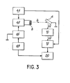
- the filament 8 constituting the electron source, is heated in a pulsed manner by means of a heating device 42 controlled by a pulsation circuit 44 whose purpose is also to block and unblock the detector 12. Furthermore, the filament is brought to a certain potential V with respect to the sample 4 by means of a device 46 serving. apply the initial energy E i to the electrons bombarding the sample 4.
- the heating is cut by means of the control circuit 44 so that the filament is equipotential.
- the interruption of heating unlocks the counting (for 8 ms) by means of the detector 12 of photons of the same energy selected by the monochromator 10 ..
- the device 46 is connected to a control circuit 48 making it possible to carry out a voltage sweep, therefore to modify the energy Ei of the electrons, when photons of the same energy are detected.
- the control circuit 48 and the detector 12 are connected to a multichannel selector 50, which makes it possible to obtain the isochromatic spectrum due to braking radiation or BIS spectrum for the detection of photons of the same energy.
- FIG. 4 An example of the BIS spectrum is shown in FIG. 4, and gives as a first approximation the number of the unoccupied electronic states n (E f ) as a function of the energy Ei of the electrons expressed in electron volts (eV).
- This spectrum is that of platinum for photons having an energy of 24.8 electrons-volts or a wavelength of 500 A; curve a represents the experimental curve, and curve b represents the theoretical curve.
- the dimension of the input slit 38 can be modified as a function of the incident energy Ei of the electrons by means of a control device 52. Indeed, for the low energies of the incident electrons (less than 20 eV) the electronic emission current is low and it is necessary to open the slots of the monochromator, which modifies little the energy resolution in this area but increases the counting rate. On the other hand, for energies high, the emission current increases strongly, so the counting rate too and, we can afford to work with narrower slits which increases the resolution.
- the slit input 38 will be 0.1 mm for an energy of 50eV, while it will be 0.6 mm for an energy of 20eV.
- this device is very convenient to use. Indeed, the monochromator measures only 60 cm, which is very compact. Furthermore, its positioning relative to the sample is easy to perform by means of the bellows 20 integral with the tube 26 of the monochromator 10. In addition, the optical adjustment of the network poses no problem.
- the device of the invention makes it possible to establish for a given material the fluorescent spectrum ultraviolet rescence of said excited material. by electrons.
- This spectrum is established by bombarding the sample by means of an electron beam of fixed energy and by detecting the photons emitted by carrying out a scanning in wavelength of these photons. This is very possible by means of the mobile network, the rotation of which can be controlled by a stepping motor.
- the electron bombardment serves to excite a bonded electron of the material by making it pass from an energy state Ea to an energy state E b higher than the Fermi E F level .
- the UV fluorescence spectrum is characteristic of the sample, which makes it possible to control its composition.
- An example for platinum has been shown in Figure 5.
- the wavelengths A expressed in A are plotted on the abscissa and the number of photons P emitted by fluorescence from a platinum sample excited by electrons of fixed energy and equal to 500 eV is plotted on the ordinate.
- the doublet observed 5P 1/2 and 5P 3/2 corresponds to the de-excitation of the vacancies created in the atomic sublayers 5P 1/2 and 5 P 3 / 2-
- the study of the BIS spectrum should make it possible to study the phenomena of absorption, corrosion and oxidation of a material.
- the fraction of the band gap between E F and the first unoccupied states can be determined directly on the spectra.
Landscapes
- Physics & Mathematics (AREA)
- Health & Medical Sciences (AREA)
- Life Sciences & Earth Sciences (AREA)
- Chemical & Material Sciences (AREA)
- Analytical Chemistry (AREA)
- Biochemistry (AREA)
- General Health & Medical Sciences (AREA)
- General Physics & Mathematics (AREA)
- Immunology (AREA)
- Pathology (AREA)
- Analysing Materials By The Use Of Radiation (AREA)
- Investigating, Analyzing Materials By Fluorescence Or Luminescence (AREA)
Applications Claiming Priority (2)
| Application Number | Priority Date | Filing Date | Title |
|---|---|---|---|
| FR8109613A FR2506019A1 (fr) | 1981-05-14 | 1981-05-14 | Dispositif pour determiner la densite des etats electroniques inoccupes d'un materiau situes au-dessus du niveau de fermi |
| FR8109613 | 1981-05-14 |
Publications (3)
| Publication Number | Publication Date |
|---|---|
| EP0065456A2 true EP0065456A2 (de) | 1982-11-24 |
| EP0065456A3 EP0065456A3 (en) | 1983-08-03 |
| EP0065456B1 EP0065456B1 (de) | 1986-09-03 |
Family
ID=9258441
Family Applications (1)
| Application Number | Title | Priority Date | Filing Date |
|---|---|---|---|
| EP82400834A Expired EP0065456B1 (de) | 1981-05-14 | 1982-05-06 | Vorrichtung zur Bestimmung der Dichte von nichtbesetzten Elektronenschalen eines Materials, die sich oberhalb des Fermi-Standes befinden |
Country Status (4)
| Country | Link |
|---|---|
| US (1) | US4472634A (de) |
| EP (1) | EP0065456B1 (de) |
| DE (1) | DE3272985D1 (de) |
| FR (1) | FR2506019A1 (de) |
Cited By (1)
| Publication number | Priority date | Publication date | Assignee | Title |
|---|---|---|---|---|
| EP0475305A3 (en) * | 1990-09-10 | 1992-10-21 | Shimadzu Corporation | Apparatus and method for inverse photoemission spectroscopy |
Families Citing this family (2)
| Publication number | Priority date | Publication date | Assignee | Title |
|---|---|---|---|---|
| DE3741675A1 (de) * | 1987-12-09 | 1989-06-22 | Kernforschungsanlage Juelich | Detektor fuer bremsstrahlungs-isochromaten-spektroskopie |
| JP2636113B2 (ja) * | 1992-03-26 | 1997-07-30 | 広島大学長 | 帯域フィルター型逆光電子分光検出装置 |
Family Cites Families (2)
| Publication number | Priority date | Publication date | Assignee | Title |
|---|---|---|---|---|
| US4253765A (en) * | 1978-02-22 | 1981-03-03 | Hitachi, Ltd. | Multi-wavelength spectrophotometer |
| NL7806330A (nl) * | 1978-06-12 | 1979-12-14 | Philips Nv | Roentgenspektrometer. |
-
1981
- 1981-05-14 FR FR8109613A patent/FR2506019A1/fr active Granted
-
1982
- 1982-04-29 US US06/373,240 patent/US4472634A/en not_active Expired - Fee Related
- 1982-05-06 EP EP82400834A patent/EP0065456B1/de not_active Expired
- 1982-05-06 DE DE8282400834T patent/DE3272985D1/de not_active Expired
Cited By (1)
| Publication number | Priority date | Publication date | Assignee | Title |
|---|---|---|---|---|
| EP0475305A3 (en) * | 1990-09-10 | 1992-10-21 | Shimadzu Corporation | Apparatus and method for inverse photoemission spectroscopy |
Also Published As
| Publication number | Publication date |
|---|---|
| DE3272985D1 (en) | 1986-10-09 |
| FR2506019A1 (fr) | 1982-11-19 |
| US4472634A (en) | 1984-09-18 |
| FR2506019B1 (de) | 1984-07-13 |
| EP0065456A3 (en) | 1983-08-03 |
| EP0065456B1 (de) | 1986-09-03 |
Similar Documents
| Publication | Publication Date | Title |
|---|---|---|
| Shelkovenko et al. | Time-resolved spectroscopic measurements of∼ 1 keV, dense, subnanosecond X-pinch plasma bright spots | |
| Iida et al. | Synchrotron radiation excited X-ray fluorescence analysis using total reflection of X-rays | |
| Wainfan et al. | Preliminary results on photoelectric yields of Pt and Ta and on photoionization in O2 and N2 in the vacuum ultraviolet | |
| Allen et al. | Early stages in the oxidation of magnesium, aluminium and magnesium/aluminium alloys: I. Exoelectron emission and long wavelength photoemission | |
| EP0065456B1 (de) | Vorrichtung zur Bestimmung der Dichte von nichtbesetzten Elektronenschalen eines Materials, die sich oberhalb des Fermi-Standes befinden | |
| EP3583447A1 (de) | Verfahren zur kalibrierung eines gamma-spektrometers und vorrichtung zur ermöglichung solch einer kalibrierung | |
| EP3492950B1 (de) | Verfahren zur kalibrierung eines gammaspektrometers, entsprechendes kalibrierungssystem und entsprechende gammaspektrometrieeinheit | |
| CA1245374A (fr) | Generateur de rayon x | |
| JP2982262B2 (ja) | 逆光電子分光装置 | |
| Butler et al. | Emission spectral analysis with the glow discharge source and a resonance detector | |
| Maeda et al. | GaSb-growth study by realtime crystal-growth analysis system using synchrotron radiation photoelectron spectroscopy | |
| FR2601778A1 (fr) | Dispositif de dosage elementaire en milieu radioactif par fluorescence induite par laser dans un plasma haute frequence | |
| EP1490888B1 (de) | Einrichtung zur messung der emission von röntgenstrahlen, die durch ein objekt erzeugt werden, das einem elektronenstrahl ausgesetzt ist | |
| Fujikawa et al. | In situ calibration of a flat-field grazing incidence spectrograph with an x-ray charge-coupled device camera using a transmission grating and a laser-produced plasma for x-ray laser research | |
| EP0270589A1 (de) | Gerät und verfahren zur chemischen analyse von festkörpern mittels durch röntgenstrahlen angeregter photoelektronen | |
| Bedo et al. | Collimating grating monochromators for the vacuum ultraviolet | |
| US5796101A (en) | Method of processing nucleic acids | |
| Wallace et al. | Testing the optical components for the NIF time-resolved soft x-ray opacity spectrometer (OpSpecTR) | |
| Pronko et al. | Emission spectra characteristics and selective filtering studies of organic scintillators | |
| Salanave | The optical spectrum of lightning | |
| Munakata et al. | Laser based photoelectron spectromicroscope | |
| FR2602058A1 (fr) | Detecteur a gaz utilisant une anode a microbandes | |
| Hartman | Recent instrumentation for the optical studies of solids in the vacuum ultra-violet | |
| EP4333018A1 (de) | Verfahren und system zur kalibrierung eines spektrometers für geladene teilchen | |
| Tomov et al. | Ultrafast time-resolved EXAFS spectroscopy using an energy dispersive spectrometer |
Legal Events
| Date | Code | Title | Description |
|---|---|---|---|
| PUAI | Public reference made under article 153(3) epc to a published international application that has entered the european phase |
Free format text: ORIGINAL CODE: 0009012 |
|
| AK | Designated contracting states |
Designated state(s): DE GB |
|
| PUAL | Search report despatched |
Free format text: ORIGINAL CODE: 0009013 |
|
| AK | Designated contracting states |
Designated state(s): DE GB |
|
| 17P | Request for examination filed |
Effective date: 19840102 |
|
| GRAA | (expected) grant |
Free format text: ORIGINAL CODE: 0009210 |
|
| AK | Designated contracting states |
Kind code of ref document: B1 Designated state(s): DE GB |
|
| REF | Corresponds to: |
Ref document number: 3272985 Country of ref document: DE Date of ref document: 19861009 |
|
| PLBE | No opposition filed within time limit |
Free format text: ORIGINAL CODE: 0009261 |
|
| STAA | Information on the status of an ep patent application or granted ep patent |
Free format text: STATUS: NO OPPOSITION FILED WITHIN TIME LIMIT |
|
| 26N | No opposition filed | ||
| PG25 | Lapsed in a contracting state [announced via postgrant information from national office to epo] |
Ref country code: GB Effective date: 19890506 |
|
| GBPC | Gb: european patent ceased through non-payment of renewal fee | ||
| PG25 | Lapsed in a contracting state [announced via postgrant information from national office to epo] |
Ref country code: DE Effective date: 19900201 |