EP0065596A2 - Signal decoder - Google Patents
Signal decoder Download PDFInfo
- Publication number
- EP0065596A2 EP0065596A2 EP81109272A EP81109272A EP0065596A2 EP 0065596 A2 EP0065596 A2 EP 0065596A2 EP 81109272 A EP81109272 A EP 81109272A EP 81109272 A EP81109272 A EP 81109272A EP 0065596 A2 EP0065596 A2 EP 0065596A2
- Authority
- EP
- European Patent Office
- Prior art keywords
- input
- output
- signal
- switch
- wave
- Prior art date
- Legal status (The legal status is an assumption and is not a legal conclusion. Google has not performed a legal analysis and makes no representation as to the accuracy of the status listed.)
- Granted
Links
Images


Classifications
-
- H—ELECTRICITY
- H04—ELECTRIC COMMUNICATION TECHNIQUE
- H04L—TRANSMISSION OF DIGITAL INFORMATION, e.g. TELEGRAPHIC COMMUNICATION
- H04L25/00—Baseband systems
- H04L25/38—Synchronous or start-stop systems, e.g. for Baudot code
- H04L25/40—Transmitting circuits; Receiving circuits
- H04L25/49—Transmitting circuits; Receiving circuits using code conversion at the transmitter; using predistortion; using insertion of idle bits for obtaining a desired frequency spectrum; using three or more amplitude levels ; Baseband coding techniques specific to data transmission systems
- H04L25/4917—Transmitting circuits; Receiving circuits using code conversion at the transmitter; using predistortion; using insertion of idle bits for obtaining a desired frequency spectrum; using three or more amplitude levels ; Baseband coding techniques specific to data transmission systems using multilevel codes
- H04L25/4923—Transmitting circuits; Receiving circuits using code conversion at the transmitter; using predistortion; using insertion of idle bits for obtaining a desired frequency spectrum; using three or more amplitude levels ; Baseband coding techniques specific to data transmission systems using multilevel codes using ternary codes
- H04L25/4925—Transmitting circuits; Receiving circuits using code conversion at the transmitter; using predistortion; using insertion of idle bits for obtaining a desired frequency spectrum; using three or more amplitude levels ; Baseband coding techniques specific to data transmission systems using multilevel codes using ternary codes using balanced bipolar ternary codes
Definitions
- the invention relates to a signal decoder for converting a codirectional 64 kbit / s interface signal divided and amplified into a positive and a negative half wave into a binary information signal, into a 64 kHz clock and into an 8 kHz clock.
- Such interface signals are defined in the CCITT Orange Book, Vol. 111-2, Line Transmission, 1977, pages 432-433, G. 732 or page 458-459, G.744.
- the object of the invention is to implement such a signal decoder.
- this object is achieved according to the invention in that a first memory is provided for each half-wave, the input of which is connected via a first switch to the input for the half-wave, and a second memory is provided for each half-wave, the input of which is connected to the output of a second switch, the control input of which is in turn connected to the output of a controllable inverter, the input of which is also connected to the input for the half-wave and the control input of which is connected to the output of the first memory, that for each half-wave.
- a third memory is provided, the input of which is connected to the output of a third switch, the control input of which is in turn connected to the input for the half-wave, that for each half-wave a counter is provided, the start input of which is connected to the input for the first half-wave, the stop input of which is connected to the input of the second half-wave, the first command output of which is connected to the control input of the first switch, the second command output of which is connected to the input of the second switch and whose third command output is connected to the input of the third switch, that a first OR gate is provided, the inputs of which are connected to an output of each of the first memories and the output of which outputs the information signal that a second OR gate is provided, the inputs of which are each connected to an output of the second memory and the output of which outputs the 64 kHz clock, and that a third OR gate is provided, the inputs of which are connected to an output of the third memory and the output of which is the 8 kHz clock delivers.
- the decoded signal is derived exclusively from the edges of the input signal.
- the closing phase of the first switch is 3/8
- the closing phase of the second switch is 1/2
- the signal decoder according to the invention can advantageously be used in the data inputs of the PCM 30 F system, a PCM switch or a 64 kbit / s terminal.
- Fig. 1 shows the stages for forming the codirectional interface signal.
- Line a shows the bit number
- line b shows the states of the 64 kbit / s signal
- line c shows a signal in which the state zero by a code word "1010” and the state one by a code word " 1100 "is formed.
- Line d also shows a signal in which these code words are alternately reversed.
- Line e shows this signal in which every eighth code word violates the inversion rule. These digits are identified by 7.
- Line f finally shows an 8 kHz signal.
- FIG. 2 shows a signal decoder according to the invention.
- the arrangement contains an input 1, switches 2, 5 and 7, a controllable inverter 4, memories 3, 6 and 8 and a counter 9 for a half-wave.
- a corresponding arrangement for the other half-wave is identified with the same reference numerals but with an apostrophe.
- the outputs of the memories are combined by OR gates 10, 11 and 12.
- the counters 9 and 9 ' have a start input 14, 14', a stop input 15, 15 ', a first command output 16, 16', a second command output 17, 17 ', a third command output 18, 18' and a clock input 13.
- Fig. 3 shows a practical embodiment of the signal decoder according to Fig. 2.
- the counter 9 consists of a divider (8: 1) 91, an inverter 92 and three stages 93, 94 and 95 of an internal counter.
- the RS memory 22, 22 ' forms the start / stop commands for both counters 9, 9'.
- the memory outputs are linked by gates 24, 25 and 26, which perform an OR function.
Landscapes
- Physics & Mathematics (AREA)
- Spectroscopy & Molecular Physics (AREA)
- Engineering & Computer Science (AREA)
- Computer Networks & Wireless Communication (AREA)
- Signal Processing (AREA)
- Analogue/Digital Conversion (AREA)
- Synchronisation In Digital Transmission Systems (AREA)
- Dc Digital Transmission (AREA)
- Circuits Of Receivers In General (AREA)
- Selective Calling Equipment (AREA)
- Error Detection And Correction (AREA)
- Compression, Expansion, Code Conversion, And Decoders (AREA)
Abstract
Die Erfindung bezieht sich auf einen Signaldecoder zum Umsetzen eines codirektionalen, in Halbwellen aufgeteilten 64-kbits-Schnittstellensignals in ein binäres Informationssignal, in einen 64-kHz-Takt und in einen 8-kHz-Takt. Erfindungsgemäß sind für jede Halbwelle eine Anordnung vorgesehen, in der Kriterien des zu dekodierenden Signals in drei Speicher (3, 6, 8 bzw. 3', 6', 8') zu Zeitpunkten eingegeben werden, die ein Zähler (9 bzw. 9') angibt. Die Zustände an den Ausgängen korrespondierender Speicher (3, 3'; 6,6'; 8,8') werden durch ODER-Gatter (10, 11, 12) zusammengefaßt. An ihren Ausgängen (10, 11, 12) sind die dekodierten Signale entnehmbar. Der Signaldecoder ist in den Datensignaleingängen des Systems PCM 30 F, einer PCM-Vermittlung oder eines 64-kbit/s-Endgerätes einsetzbar (Fig. 2).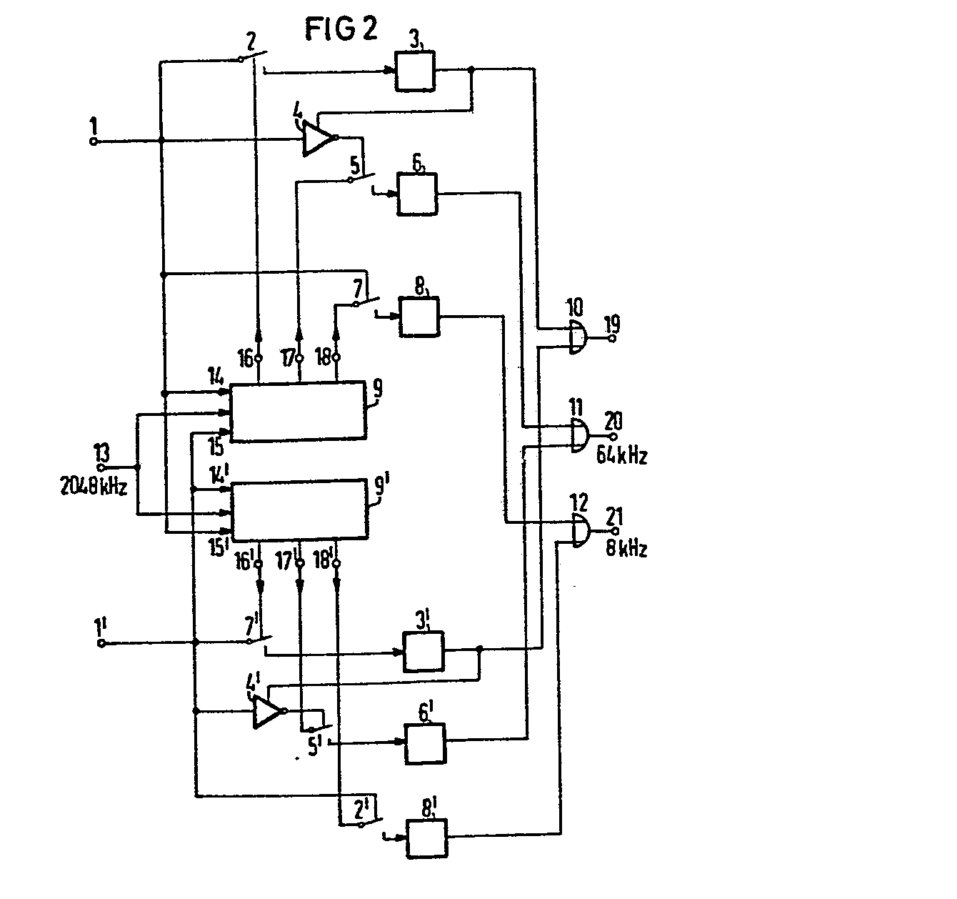
Description
Die Erfindung bezieht sich auf einen Signaldecoder zur Umsetzung eines codirektionalen, in eine positive und eine negative Halbwelle geteiltes und verstärktes 64-kbit/s-Schnittstellensignal in ein binäres Informationssignal, in einen 64-kHz-Takt und in einen 8-kHz-Takt.The invention relates to a signal decoder for converting a codirectional 64 kbit / s interface signal divided and amplified into a positive and a negative half wave into a binary information signal, into a 64 kHz clock and into an 8 kHz clock.
Derartige Schnittstellensignale sind im CCITT Orange-Book, Vol. 111-2, Line Transmission, 1977, Seiten 432-433, G. 732 oder Seite 458-459, G.744, definiert.Such interface signals are defined in the CCITT Orange Book, Vol. 111-2, Line Transmission, 1977, pages 432-433, G. 732 or page 458-459, G.744.
Der Erfindung liegt die Aufgabe zugrunde, einen derartigen Signaldecoder zu realisieren.The object of the invention is to implement such a signal decoder.
Ausgehend von einem Signaldecoder der einleitend geschilderten Art wird diese Aufgabe erfindungsgemäß dadurch gelöst, daß für jede Halbwelle ein erster Speicher vorgesehen ist, dessen Eingang über einen ersten Schalter mit dem Eingang für die Halbwelle verbunden ist, daß für jede Halbwelle ein zweiter Speicher vcrgesehen ist, dessen Eingang mit dem Ausgang eines zweiten Schalters verbunden.ist, dessen Steuereingang wiederum mit dem Ausgang eines steuerbaren Inverters verbunden ist, dessen Eingang außerdem mit dem Eingang für die Halbwelle und dessen Steuereingang mit dem Ausgang des ersten Speichers verbunden ist, daß für jede Halbwelle.ein dritter Speicher vorgesehen ist, dessen Eingang mit dem Ausgang eines dritten Schalters verbunden ist, dessen Steuereingang wiederum mit den Eingang für die Halbwelle verbunden ist, daß für jede Halbwelle ein Zähler vorgesehen ist, dessen Starteingang mit dem Eingang für die erste Halbwelle verbunden ist, dessen Stoppeingang mit dem Eingang für die zweite Halbwelle verbunden ist, dessen erster Befehlsausgang mit dem Steuereingang des ersten Schalters verbunden ist, dessen zweiter Befehlsausgang mit dem Eingang des zweiten Schalters und dessen dritter Befehlsausgang mit dem Eingang des dritten Schalters verbunden ist, daß ein erstes ODER-Gatter vorgesehen ist, dessen Eingänge mit jeweils einem Ausgang der ersten Speicher verbundensind und dessen Ausgang das Informationssignal abgibt, daß ein zweites ODER-Gatter vorgesehen ist, dessen Eingänge mit jeweils einen Ausgang der zweiten Speicher verbunden sind und dessen Ausgang den 64-kHz-Takt abgibt,und daß ein drittes ODER-Gatter vorgesehen ist, dessen Eingänge mit jeweils einem Ausgang der dritten Speicher verbunden sind und dessen Ausgang den 8-kHz-Takt abgibt.Starting from a signal decoder of the type described in the introduction, this object is achieved according to the invention in that a first memory is provided for each half-wave, the input of which is connected via a first switch to the input for the half-wave, and a second memory is provided for each half-wave, the input of which is connected to the output of a second switch, the control input of which is in turn connected to the output of a controllable inverter, the input of which is also connected to the input for the half-wave and the control input of which is connected to the output of the first memory, that for each half-wave. a third memory is provided, the input of which is connected to the output of a third switch, the control input of which is in turn connected to the input for the half-wave, that for each half-wave a counter is provided, the start input of which is connected to the input for the first half-wave, the stop input of which is connected to the input of the second half-wave, the first command output of which is connected to the control input of the first switch, the second command output of which is connected to the input of the second switch and whose third command output is connected to the input of the third switch, that a first OR gate is provided, the inputs of which are connected to an output of each of the first memories and the output of which outputs the information signal that a second OR gate is provided, the inputs of which are each connected to an output of the second memory and the output of which outputs the 64 kHz clock, and that a third OR gate is provided, the inputs of which are connected to an output of the third memory and the output of which is the 8 kHz clock delivers.
Bei dieser Lösung wird das decodierte Signal ausschließlich aus den Flanken des Eingangssignals abgeleitet.In this solution, the decoded signal is derived exclusively from the edges of the input signal.
Für eine Decodierung eines Schnittstellensignals nach CCITT G.732 ist es vorteilhaft, wenn dreistufige binäre interne Zähler vorgesehen sind, deren Stufenausgänge mit den Befehlsausgängen der Zähler verbunden sind, und wenn Teiler 8:1 vorgesehen sind, an deren Eingängen der Systemtakt 2048 kHz angeschlossen ist und deren invertierte Ausgänge mit den Takteingängen der internen Zähler verbunden sind.For decoding an interface signal according to CCITT G.732, it is advantageous if three-stage binary internal counters are provided, the stage outputs of which are connected to the command outputs of the counters, and if dividers 8: 1 are provided, the inputs of which are connected to the 2048 kHz system clock and whose inverted outputs are connected to the clock inputs of the internal counters.
Dabei ist es vorteilhaft, wenn die Schließungsphase des ersten Schalters bei 3/8, die Schließungsphase des zweiten Schalters bei 1/2 und die Schließungsphase des dritten Schalters bei = 1 der Dauer der Codewörter für die Zustände Null und Eins liegen.It is advantageous if the closing phase of the first switch is 3/8, the closing phase of the second switch is 1/2 and the closing phase of the third switch is = 1 the duration of the code words for the states zero and one.
Für die Decodierung eines Schnittstellensignals nach CCITT G.744 ist es vorteilhaft, wenn dreistufige binäre Zähler vorgesehen sind, deren Stufenausgänge mit den Befehlsausgängen der Zähler verbunden sind, und.wenn Teiler vorgesehen sind, an deren Eingängen der Systemtakt 8448 kHz angeschlossen ist und deren invertierte Ausgänge mit den Takteingängen der internen Zähler verbunden sind.For decoding an interface signal according to CCITT G.744, it is advantageous if three-stage binary counters are provided, the stage outputs of which are connected to the command outputs of the counters, and if dividers are provided whose inputs have the system clock 8448 kHz connected and their inverted ones Outputs are connected to the clock inputs of the internal counter.
Der erfindungsgemäße Signaldecoder ist in vorteilhafter Weise in den Dateneingängen des Systems PCM 30 F, einer PCM-Vermittlung oder eines 64-kbit/s-Endgerätes verwendbar.The signal decoder according to the invention can advantageously be used in the data inputs of the PCM 30 F system, a PCM switch or a 64 kbit / s terminal.
Anhand von Ausführungsbeispielen wird die Erfindung nachstehend näher erläutert.The invention is explained in more detail below on the basis of exemplary embodiments.
- Fig. 1 zeigt ein Schnittstellensignal nach CCITT G.732,1 shows an interface signal according to CCITT G.732,
- Fig. 2 zeigt einen erfindungsgemäßen Signaldecoder,2 shows a signal decoder according to the invention,
- Fig. 3 zeigt eine praktische Ausführung des erfindungsgemäßen Signaldecoders undFig. 3 shows a practical embodiment of the signal decoder and
- Fig. 4 zeigt einen Pulsplan zum Signaldecoder nach Fig. 3.FIG. 4 shows a pulse schedule for the signal decoder according to FIG. 3.
Fig. 1 zeigt die Stufen zur Bildung des codirektionalen Schnittstellensignales. Die Zeile a zeigt die Bit-Nummer, die Zeile b zeigt die Zustände des 64-kbit/s-Signals und die Zeile c zeigt ein Signal, in dem der Zustand Null durch ein Codewort "1010" und der Zustand Eins durch ein Codewort "1100" gebildet wird. Die Zeile d zeigt weiter ein Signal, bei dem diese Codewörter alternierend umgepolt werden. Zeile e zeigt dieses Signal, in dem jedes achte Codewort die Umkehrregel verletzt. Diese Stellen sind durch 7 gekennzeichnet. Zeile f zeigt schließlich ein 8-kHz-Signal.Fig. 1 shows the stages for forming the codirectional interface signal. Line a shows the bit number, line b shows the states of the 64 kbit / s signal and line c shows a signal in which the state zero by a code word "1010" and the state one by a code word " 1100 "is formed. Line d also shows a signal in which these code words are alternately reversed. Line e shows this signal in which every eighth code word violates the inversion rule. These digits are identified by 7. Line f finally shows an 8 kHz signal.
Fig. 2 zeigt einen erfindungsgemäßen Signaldecoder. Die Anordnung enthält für eine Halbwelle einen Eingang 1, Schalter 2, 5 und 7, einen steuerbaren Inverter 4, Speicher 3, 6 und 8 sowie einen Zähler 9. Eine entsprechende Anordnung für die andere Halbwelle ist mit denselben Bezugszeichen aber mit einem Apostroph gekennzeichnet. Die Ausgänge der Speicher sind durch ODER-Gatter 10, 11 und 12 zusammengefaßt.2 shows a signal decoder according to the invention. The arrangement contains an
Die Zähler 9 und 9' weisen einen Starteingang 14, 14', einen Stoppeingang 15, 15', einen ersten Befehlsausgang 16, 16', einen zweiten Befehlsausgang 17, 17', einen dritten Befehlsausgang 18, 18' und einen Takteingang 13 auf.The counters 9 and 9 'have a
Die Wirkungsweise des Signaldecoders nach Fig. 2 wird unter zuhilfenahme des Pulsplanes nach Fig. 4 näher erhläutert. An den Eingang 1 wird eine Halbwelle angelegt. Der Schalter 2 schließt gesteuert vom Signal am Befehlsausgang 16 zu den Zeitpunkten t1. Der in diesem Moment in der Halbwelle bestehende Zustand wird im Speicher 3 festgehalten. Am Befehlsausgang 17 liegt der Zustand vom Ausgang einer zweiten Stufe des Zählers 9 an. Dieser wird über den Schalter 5 zum Zeitpunkt t2 an den Speicher 6 gegeben. Dieser Schalter 5 wird mit dem Signal am Eingang 1 geschlossen, wobei der Zustand am Ausgang des Speichers 3 gewährleistet, daß nur Signalflanken einer Art am Ausgang des gesteuerten Inverters 4 wirksam werden. Der Zustand am Befehlsausgang 18, der aus Figur 4 ersichtlich ist, wird über den Schalter 7 zum Zeitpunkt t3 auf den Speicher 8 immer dann gegeben, wenn am Eingang 1 Signalflanken einer Art auftreten. Der beschriebene Vorgang läuft in gleicher Weise in der zweiten Hälfte der Schaltung ab, wenn an den Eingang 1' die andere Halbwelle angelegt wird.The mode of operation of the signal decoder according to FIG. 2 is explained in more detail with the aid of the pulse plan according to FIG. 4. A half wave is applied to
Ein alternierendes Arbeiten beider Anordnungshälften wird durch die Start/Stopp-Signale an den Eingängen 14 und 15 bzw. 14' und 15' bewirkt. An den ODER-Gattern 10, 11, 12 werden die Signale der korrespondierenden'Speicher 3 und 3', 6 und 6', 8 und 8' zusammengefaßt. Am Ausgang 19 erscheint das decodierte Informationssignal, am Ausgang 20 tritt ein 64-kHz-Takt und am Ausgang 21 ein 8-kHz-Takt auf.An alternating working of both arrangement halves is brought about by the start / stop signals at the
Fig. 3 zeigt eine praktische Ausführung des Signaldecoders nach Fig. 2. Der Zähler 9 besteht aus einem Teiler (8:1) 91, einem Inverter 92 und drei Stufen 93, 94 und 95 eines internen Zählers. Der RS-Speicher 22, 22' bildet die Start/Stopp-Befehle für beide Zähler 9, 9'. Die Verknüpfung der Speicherausgänge erfolgt durch die Gatter 24, 25 und 26, die eine ODER-Funktion ausüben.Fig. 3 shows a practical embodiment of the signal decoder according to Fig. 2. The counter 9 consists of a divider (8: 1) 91, an
Die Wirkungsweise des Signaldecoders nach Fig. 3 läßt sich mit Hilfe des Pulsplans in Fig. 4 anhand der aufgeführten Schaltungspunkte verfolgen.The mode of operation of the signal decoder according to FIG. 3 can be followed with the aid of the pulse plan in FIG. 4 using the circuit points listed.
Claims (7)
Applications Claiming Priority (2)
| Application Number | Priority Date | Filing Date | Title |
|---|---|---|---|
| DE3120282 | 1981-05-21 | ||
| DE19813120282 DE3120282A1 (en) | 1981-05-21 | 1981-05-21 | SIGNAL DECODER |
Publications (3)
| Publication Number | Publication Date |
|---|---|
| EP0065596A2 true EP0065596A2 (en) | 1982-12-01 |
| EP0065596A3 EP0065596A3 (en) | 1984-02-22 |
| EP0065596B1 EP0065596B1 (en) | 1986-02-26 |
Family
ID=6132915
Family Applications (1)
| Application Number | Title | Priority Date | Filing Date |
|---|---|---|---|
| EP81109272A Expired EP0065596B1 (en) | 1981-05-21 | 1981-10-29 | Signal decoder |
Country Status (6)
| Country | Link |
|---|---|
| US (1) | US4473820A (en) |
| EP (1) | EP0065596B1 (en) |
| JP (1) | JPS57197946A (en) |
| BR (1) | BR8202935A (en) |
| DE (2) | DE3120282A1 (en) |
| NO (1) | NO158979C (en) |
Families Citing this family (2)
| Publication number | Priority date | Publication date | Assignee | Title |
|---|---|---|---|---|
| US5684833A (en) * | 1994-04-21 | 1997-11-04 | Aichidenshi Kabushiki Kaisha | Mutual conversion method of binary data and multilevel signal, its communication method, and its receiving device |
| DE10132048A1 (en) * | 2001-07-03 | 2003-01-23 | Siemens Ag | Output unit, receiving unit, arrangement for data transmission in a motor vehicle and method therefor |
Family Cites Families (4)
| Publication number | Priority date | Publication date | Assignee | Title |
|---|---|---|---|---|
| US3787613A (en) * | 1972-06-27 | 1974-01-22 | Bell Telephone Labor Inc | Pulse transmission system for conveying data and control words by means of alternating polarity pulses and violations thereof |
| US3745361A (en) * | 1972-06-27 | 1973-07-10 | Bell Telephone Labor Inc | Composite clock signal generating and distributing circuits |
| FR2407617A1 (en) * | 1977-10-28 | 1979-05-25 | Telecommunications Sa | PROCESS FOR RECEIVING 64 KBIT / S CODIRECTIONAL JUNCTIONS AND ITS IMPLEMENTATION DEVICE |
| US4380080A (en) * | 1980-12-30 | 1983-04-12 | Sperry Corporation | Tri-level differential line receiver |
-
1981
- 1981-05-21 DE DE19813120282 patent/DE3120282A1/en not_active Withdrawn
- 1981-10-29 EP EP81109272A patent/EP0065596B1/en not_active Expired
- 1981-10-29 DE DE8181109272T patent/DE3173902D1/en not_active Expired
-
1982
- 1982-04-14 US US06/368,450 patent/US4473820A/en not_active Expired - Fee Related
- 1982-05-19 NO NO821664A patent/NO158979C/en unknown
- 1982-05-20 BR BR8202935A patent/BR8202935A/en unknown
- 1982-05-20 JP JP57084132A patent/JPS57197946A/en active Pending
Also Published As
| Publication number | Publication date |
|---|---|
| EP0065596A3 (en) | 1984-02-22 |
| NO158979C (en) | 1988-11-16 |
| JPS57197946A (en) | 1982-12-04 |
| NO158979B (en) | 1988-08-08 |
| US4473820A (en) | 1984-09-25 |
| DE3173902D1 (en) | 1986-04-03 |
| EP0065596B1 (en) | 1986-02-26 |
| NO821664L (en) | 1982-11-22 |
| DE3120282A1 (en) | 1982-12-09 |
| BR8202935A (en) | 1983-05-03 |
Similar Documents
| Publication | Publication Date | Title |
|---|---|---|
| DE2608902C3 (en) | Code converter device | |
| DE3544820A1 (en) | SWITCHING FREQUENCY DIVISION | |
| DE69113286T2 (en) | Operation and control of a circuit breaker. | |
| CH620068A5 (en) | ||
| DE2950806C2 (en) | ||
| DE2943036A1 (en) | Surface acoustic wave unique word detector and coherent demodulator | |
| EP0019821B1 (en) | Method and device for transmitting a binary sequence | |
| DE2618633C3 (en) | PCM decoder | |
| EP0065596A2 (en) | Signal decoder | |
| DE68922506T2 (en) | Frequency divider circuit. | |
| EP0048352A1 (en) | Binary MOS-switched carry parallel adder | |
| DE3018509A1 (en) | SLIDE REGISTER WITH LATCH SWITCHING | |
| DE2133660A1 (en) | Encoder | |
| EP0198263A2 (en) | Circuit arrangement for the ungrounded transmission of digital signals across points of isolation | |
| DE2143470A1 (en) | Code converter | |
| DE1762681A1 (en) | Pulse discriminator circuit | |
| DE1524122A1 (en) | Electronic data processing system with time allocation of memory access | |
| CH509706A (en) | Digital-to-analog converter | |
| EP0326856A1 (en) | Electronic pulse counter | |
| DE2605380C3 (en) | Circuit arrangement for generating a square wave from the mixture of two square waves with one another | |
| DE2443869A1 (en) | DIGITAL DATA TRANSFER SYSTEM | |
| DE3110891C2 (en) | Circuit arrangement for the repeated sharing of electrical charges | |
| DE3042761C2 (en) | Circuit arrangement for obtaining an electrical reference clock pulse sequence for the decoding of a multi-length writing read from a recording medium and recorded thereon | |
| DE2525533A1 (en) | Decoder for code with two or more valves - is used for ternary biphase level code without direct current and pulses are evaluated | |
| DE2811753C2 (en) | Digital demodulator on semiconductor basis |
Legal Events
| Date | Code | Title | Description |
|---|---|---|---|
| PUAI | Public reference made under article 153(3) epc to a published international application that has entered the european phase |
Free format text: ORIGINAL CODE: 0009012 |
|
| 17P | Request for examination filed |
Effective date: 19811029 |
|
| AK | Designated contracting states |
Designated state(s): BE CH DE FR GB IT NL SE |
|
| PUAL | Search report despatched |
Free format text: ORIGINAL CODE: 0009013 |
|
| AK | Designated contracting states |
Designated state(s): BE CH DE FR GB IT LI NL SE |
|
| GRAA | (expected) grant |
Free format text: ORIGINAL CODE: 0009210 |
|
| AK | Designated contracting states |
Designated state(s): BE CH DE FR GB IT LI NL SE |
|
| PG25 | Lapsed in a contracting state [announced via postgrant information from national office to epo] |
Ref country code: BE Effective date: 19860226 |
|
| PG25 | Lapsed in a contracting state [announced via postgrant information from national office to epo] |
Ref country code: SE Effective date: 19860228 |
|
| REF | Corresponds to: |
Ref document number: 3173902 Country of ref document: DE Date of ref document: 19860403 |
|
| ITF | It: translation for a ep patent filed | ||
| ET | Fr: translation filed | ||
| PLBE | No opposition filed within time limit |
Free format text: ORIGINAL CODE: 0009261 |
|
| STAA | Information on the status of an ep patent application or granted ep patent |
Free format text: STATUS: NO OPPOSITION FILED WITHIN TIME LIMIT |
|
| 26N | No opposition filed | ||
| PGFP | Annual fee paid to national office [announced via postgrant information from national office to epo] |
Ref country code: GB Payment date: 19910913 Year of fee payment: 11 |
|
| PGFP | Annual fee paid to national office [announced via postgrant information from national office to epo] |
Ref country code: FR Payment date: 19911022 Year of fee payment: 11 |
|
| ITTA | It: last paid annual fee | ||
| PG25 | Lapsed in a contracting state [announced via postgrant information from national office to epo] |
Ref country code: GB Effective date: 19921029 |
|
| PGFP | Annual fee paid to national office [announced via postgrant information from national office to epo] |
Ref country code: NL Payment date: 19921031 Year of fee payment: 12 |
|
| PGFP | Annual fee paid to national office [announced via postgrant information from national office to epo] |
Ref country code: DE Payment date: 19921216 Year of fee payment: 12 |
|
| PGFP | Annual fee paid to national office [announced via postgrant information from national office to epo] |
Ref country code: CH Payment date: 19930121 Year of fee payment: 12 |
|
| GBPC | Gb: european patent ceased through non-payment of renewal fee |
Effective date: 19921029 |
|
| PG25 | Lapsed in a contracting state [announced via postgrant information from national office to epo] |
Ref country code: FR Effective date: 19930630 |
|
| REG | Reference to a national code |
Ref country code: FR Ref legal event code: ST |
|
| PG25 | Lapsed in a contracting state [announced via postgrant information from national office to epo] |
Ref country code: LI Effective date: 19931031 Ref country code: CH Effective date: 19931031 |
|
| PG25 | Lapsed in a contracting state [announced via postgrant information from national office to epo] |
Ref country code: NL Effective date: 19940501 |
|
| NLV4 | Nl: lapsed or anulled due to non-payment of the annual fee | ||
| REG | Reference to a national code |
Ref country code: CH Ref legal event code: PL |
|
| PG25 | Lapsed in a contracting state [announced via postgrant information from national office to epo] |
Ref country code: DE Effective date: 19940701 |