EP0066041A1 - Semiconductor device including resistive elements - Google Patents
Semiconductor device including resistive elements Download PDFInfo
- Publication number
- EP0066041A1 EP0066041A1 EP82101495A EP82101495A EP0066041A1 EP 0066041 A1 EP0066041 A1 EP 0066041A1 EP 82101495 A EP82101495 A EP 82101495A EP 82101495 A EP82101495 A EP 82101495A EP 0066041 A1 EP0066041 A1 EP 0066041A1
- Authority
- EP
- European Patent Office
- Prior art keywords
- semiconductor layer
- region
- resistive region
- semiconductor device
- diffusion
- Prior art date
- Legal status (The legal status is an assumption and is not a legal conclusion. Google has not performed a legal analysis and makes no representation as to the accuracy of the status listed.)
- Granted
Links
- 239000004065 semiconductor Substances 0.000 title claims abstract description 49
- 238000009792 diffusion process Methods 0.000 claims abstract description 46
- 239000012535 impurity Substances 0.000 claims abstract description 17
- 239000000758 substrate Substances 0.000 claims abstract description 16
- 230000015572 biosynthetic process Effects 0.000 description 2
- 230000003071 parasitic effect Effects 0.000 description 2
- 230000006866 deterioration Effects 0.000 description 1
- 238000010586 diagram Methods 0.000 description 1
- 238000002955 isolation Methods 0.000 description 1
- 239000002184 metal Substances 0.000 description 1
- 229910021420 polycrystalline silicon Inorganic materials 0.000 description 1
Images

Classifications
-
- H—ELECTRICITY
- H10—SEMICONDUCTOR DEVICES; ELECTRIC SOLID-STATE DEVICES NOT OTHERWISE PROVIDED FOR
- H10D—INORGANIC ELECTRIC SEMICONDUCTOR DEVICES
- H10D1/00—Resistors, capacitors or inductors
- H10D1/40—Resistors
- H10D1/43—Resistors having PN junctions
Definitions
- the present invention relates to a semiconductor device including resistive elements.
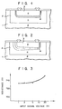
- Fig. 1 shows a model of an integrated circuit device including a diffusion resistive region.
- the integrated circuit device is comprised of a p-type semiconductor substrate 1, an isolated region 2 of n-type formed in the substrate, and a p - type diffusion resistive region 3 formed in the surface area of the isolated region 2.
- the potential of the isolated region 2 is set at a value higher than the potential of the substrate and the resistive region 3 in order to prevent the formation of parasitic elements such as pnp transistors.
- the width of a depletion layer 4 As indicated by a broken line in the drawing, which is formed in a p-n junction area between the regions 3 and 2, has a fixed value determined by a potential difference between the regions 3 and 2.
- the width of the depletion layer 4 is gradually made larger in a direction of the current flow, as indicated by a broken line in Fig. 2.
- an effective resistance of the diffusion resistive region 3 varies in accordance with a change of a signal voltage applied between both ends of the resistive region 3.
- an effective width of the depletion layer 4, i.e. the effective width of the diffusion resistive region 3 changes with the signal voltage applied to the diffusion resistive region 3, with the result that the effective resistance of the region 3 varies.
- the resistance of the diffusion resistive region varies with the signal voltage applied to the resistive region 3. Therefore, the effective resistance of.the resistive region 3 varies, leading to deterioration of the electrical performance of the integrated circuit device.
- an object of the present invention is to provide a semiconductor device including a diffusion resistive element whose effective resistance is kept substantially invariable during operation.
- a semiconductor device comprising: a semiconductor layer of one conductivity type; a diffusion resistive region of the opposite conductivity type formed in the surface area of the semiconductor layer; first and second impurity regions at higher impurity concentration than that of the semiconductor layer, the impurity regions being formed in the surface area of the semiconductor layer while sandwiching the diffusion resistive region; a current feeding device electrically coupled with the first and second impurity regions for feeding a current into the semiconductor layer in the same direction as that of current flowing into the diffusion resistive region.
- the current flows into the isolated region in the same direction as that of current flowing into the diffusion resistive region. Accordingly, a substantially fixed reverse bias voltage is applied to the pn junction between the isolated region and the diffusion region. The result is that the width of a depletion layer formed in the junction area between the isolated region and the diffusion resistive region is substantially constant. Therefore, an effective resistance of the diffusion resistive region is kept substantially constant.
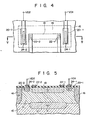
- Figs. 4 and 5 show a plan view and a cross sectional view of a semiconductor device embodying the present invention.
- the semiconductor device is comprised of a p-type substrate 10, an n +- type region 12 formed in the surface area of the substrate 10, n--type epitaxial layer 14 formed on the substrate 10 and the n +- type region 12, a p-type layer 16 formed on the substrate 10 partially surrounding the n--type region 14, and a p - -type diffusion region 18 forming a resistor which is formed in the surface area of the n--type layer 14.
- Fig. 4 and 5 show a plan view and a cross sectional view of a semiconductor device embodying the present invention.
- the semiconductor device is comprised of a p-type substrate 10, an n +- type region 12 formed in the surface area of the substrate 10, n--type epitaxial layer 14 formed on the substrate 10 and the n +- type region 12, a p-type layer 16 formed on the substrate 10 partially surrounding the n-
- n +- type regions 20-1 and 20-2 are formed in the surface area of the n - -type layer 14 and near the respective ends of the diffusion region 18, sandwiching the diffusion region 18. That is, the regions 20-l.and 20-2 are so formed that a current flows in the same direction as that of the current flowing into the diffusion region 18.
- a pair of electrodes 22-1 and 22-2 are formed in contact with both end portions of the diffusion region 18 and another pair of electrodes 24-1 and 24-2 are formed, respectively, in contact with the n +- type regions 20-1 and 20-2.
- the electrodes 24-1 and 24-2 are coupled with power source terminals VD1 and VD2, respectively.
- a power source voltage is applied between the power source terminals VDl and VD2 so as to generate in the n - -type layer 14 between the electrodes 24-1 and 24-2 a voltage drop corresponding to a signal voltage applied to the resistive region 18, that is, the signal voltage applied between the electrodes 22-1 and 22-2.
- the power source voltages VDl and VD2 (> VG) are applied to the electrodes 24-1 and 24-2.
- Fig. 6 shows a circuit for generating a voltage drop corresponding to the voltage drop of the resistive region 18 in an n--type region 14 between the electrodes 24-1 and 24-2.
- the circuit is comprised of a resistor Rl connected at one end to the power source terminal V D , and pnp transistors TR1 and TR2 whose emitter-collector paths are connected in series between the other end of the resistor R1 and ground.
- a resistor R2 corresponding to the diffusion resistive region 18 is connected between the bases of the transistors TR1 and TR2. Both ends of the resistor R2 are connected to signal input terminals SV1 and SV2 which are also connected, although not shown here, to the electrodes 22-1 and 22-2 of the semiconductor device shown in Fig. 5, the emitters of the transistors TR1 and TR2 are coupled with the electrodes 24-1 and 24-2, respectively.
- the resistances between the collectors and emitters of the transistors vary in accordance with the potentials at the signal input terminals SV1 and SV2, respectively.
- the emitter voltages of the transistors TR1 and TR2 vary in accordance with a signal voltage.
- the voltage between the base and emitter of each of the transistors TR1 and TR2 is held substantially constant. Accordingly, in the semiconductor device shown in Fig. 5, a fixed reverse bias voltage is applied between the isolated region 14 and the diffusion resistive region 18.
- the voltage between the electrodes 24-1 and 24-2 changes with a change of the signal voltage between the electrodes 22-1 and 22-2, so that the reverse bias voltage applied to the pn junction between the n--type region 14 and the resistive region 18 is always kept constant at any location of the pn junction.
- a depletion layer 25 with a fixed width is formed between the n - -type region 14 and the resistive region 18, as shown in Fig. 7.
- the width of the depletion layer is always kept at a fixed value. Therefore, it is possible to set an effective resistance of the resistive region 18 at a desired value with a high precision.
- the effective resistance of the resistive region 18 is kept substantially constant against a change of the signal voltage applied to the resistive region 18, as shown in Fig. 8. Accordingly, the electrical performance of the integrated circuit device may be improved.
- the n +- type region 12 is formed for preventing the formation of a parasitic element. This region may be omitted, if required.
- the p-type substrate used in the above-mentioned embodiment may be replaced by the n-type substrate. In this case, the other regions must be of the opposite conductivity type.
- the n--type layer 14, which is formed on the substrate 10 in the above-mentioned embodiment may be formed in the surface area of the substrate 10 when the n +- type region 12 is not formed. In this case, there is no need for forming the p-type isolation region 16.
Landscapes
- Semiconductor Integrated Circuits (AREA)
Abstract
Description
- The present invention relates to a semiconductor device including resistive elements.
- In general, resistive elements used in integrated circuit devices are formed of metal flimsy polycrystalline silicon layers, diffusion regions, etc. Of those, diffusion resistive elements are predominantly used. Fig. 1 shows a model of an integrated circuit device including a diffusion resistive region. The integrated circuit device is comprised of a p-
type semiconductor substrate 1, anisolated region 2 of n-type formed in the substrate, and a p-type diffusionresistive region 3 formed in the surface area of theisolated region 2. In the integrated circuit device, the potential of theisolated region 2 is set at a value higher than the potential of the substrate and theresistive region 3 in order to prevent the formation of parasitic elements such as pnp transistors. - When no current flows through the
resistive region 3, the width of adepletion layer 4, as indicated by a broken line in the drawing, which is formed in a p-n junction area between theregions regions resistive region 3, the width of thedepletion layer 4 is gradually made larger in a direction of the current flow, as indicated by a broken line in Fig. 2. As a result, an effective resistance of the diffusionresistive region 3 varies in accordance with a change of a signal voltage applied between both ends of theresistive region 3. In other words, an effective width of thedepletion layer 4, i.e. the effective width of the diffusionresistive region 3, changes with the signal voltage applied to the diffusionresistive region 3, with the result that the effective resistance of theregion 3 varies. - As described above, in the prior art integrated circuit device, the resistance of the diffusion resistive region varies with the signal voltage applied to the
resistive region 3. Therefore, the effective resistance of.theresistive region 3 varies, leading to deterioration of the electrical performance of the integrated circuit device. - Accordingly, an object of the present invention is to provide a semiconductor device including a diffusion resistive element whose effective resistance is kept substantially invariable during operation.
- According to one aspect of the present invention, there is provided a semiconductor device comprising: a semiconductor layer of one conductivity type; a diffusion resistive region of the opposite conductivity type formed in the surface area of the semiconductor layer; first and second impurity regions at higher impurity concentration than that of the semiconductor layer, the impurity regions being formed in the surface area of the semiconductor layer while sandwiching the diffusion resistive region; a current feeding device electrically coupled with the first and second impurity regions for feeding a current into the semiconductor layer in the same direction as that of current flowing into the diffusion resistive region.
- In the present invention, the current flows into the isolated region in the same direction as that of current flowing into the diffusion resistive region. Accordingly, a substantially fixed reverse bias voltage is applied to the pn junction between the isolated region and the diffusion region. The result is that the width of a depletion layer formed in the junction area between the isolated region and the diffusion resistive region is substantially constant. Therefore, an effective resistance of the diffusion resistive region is kept substantially constant.
- This invention can be more fully understood from the following detailed description when taken in conjunction with the accompanying drawings, in which:
- Fig. 1 illustrates a model of a prior art integrated circuit device for illustrating the state of a depletion layer formed in the junction area between an isolated region and a diffusion resistive region formed in a surface area of the isolated region when no current flows through the diffusion resistive region;
- Fig. 2 shows a model of the prior art device for illustrating the state of a depletion layer formed in the junction area between the isolated region and diffusion resistive region when a current flows into the resistive region;
- Fig. 3 shows a graph illustrating the relationship of an input signal voltage applied across the diffusion resistive region and the effective resistance of the diffusion resistive region;
- Fig. 4 shows a partial plan view of a semiconductor device which is an embodiment of the present invention;
- Fig. 5 shows a cross sectional view taken along line V - V of Fig. 4;
- Fig. 6 shows a circuit diagram of a current feed .circuit applicable for the semiconductor device shown in Figs. 4 and 5;
- Fig. 7 shows a model of a semiconductor device illustrating the state of a depletion layer formed in the junction area between a diffusion resistive region and an isolated region when the current feed circuit shown in Fig. 6 is used; and
- Fig. 8 shows a graph illustrating the relationship between an input signal voltage applied to the diffusion resistive region and the effective resistance of the diffusion resistive region when the current feed circuit shown in Fig. 6 is used.
- Figs. 4 and 5 show a plan view and a cross sectional view of a semiconductor device embodying the present invention. The semiconductor device is comprised of a p-
type substrate 10, an n+-type region 12 formed in the surface area of thesubstrate 10, n--typeepitaxial layer 14 formed on thesubstrate 10 and the n+-type region 12, a p-type layer 16 formed on thesubstrate 10 partially surrounding the n--type region 14, and a p--type diffusion region 18 forming a resistor which is formed in the surface area of the n--type layer 14. As well illustrated in Fig. 4, a pair of n+-type regions 20-1 and 20-2 are formed in the surface area of the n--type layer 14 and near the respective ends of thediffusion region 18, sandwiching thediffusion region 18. That is, the regions 20-l.and 20-2 are so formed that a current flows in the same direction as that of the current flowing into thediffusion region 18. A pair of electrodes 22-1 and 22-2 are formed in contact with both end portions of thediffusion region 18 and another pair of electrodes 24-1 and 24-2 are formed, respectively, in contact with the n+-type regions 20-1 and 20-2. - The electrodes 24-1 and 24-2 are coupled with power source terminals VD1 and VD2, respectively. A power source voltage is applied between the power source terminals VDl and VD2 so as to generate in the n--
type layer 14 between the electrodes 24-1 and 24-2 a voltage drop corresponding to a signal voltage applied to theresistive region 18, that is, the signal voltage applied between the electrodes 22-1 and 22-2. For example, in a case where the electrode 22-1 is held at a maximum signal potential VG, and a signal voltage from 0 to VG is applied between the electrodes 22-1 and 22-2, the power source voltages VDl and VD2 (> VG) are applied to the electrodes 24-1 and 24-2. In this case, it is preferable to set a difference voltage (VDl - VD2) between the electrodes 24-1 and 24-2 at a value of approximately VG/2. - Fig. 6 shows a circuit for generating a voltage drop corresponding to the voltage drop of the
resistive region 18 in an n--type region 14 between the electrodes 24-1 and 24-2. The circuit is comprised of a resistor Rl connected at one end to the power source terminal VD, and pnp transistors TR1 and TR2 whose emitter-collector paths are connected in series between the other end of the resistor R1 and ground. A resistor R2 corresponding to the diffusionresistive region 18 is connected between the bases of the transistors TR1 and TR2. Both ends of the resistor R2 are connected to signal input terminals SV1 and SV2 which are also connected, although not shown here, to the electrodes 22-1 and 22-2 of the semiconductor device shown in Fig. 5, the emitters of the transistors TR1 and TR2 are coupled with the electrodes 24-1 and 24-2, respectively. - The resistances between the collectors and emitters of the transistors vary in accordance with the potentials at the signal input terminals SV1 and SV2, respectively. As a result, the emitter voltages of the transistors TR1 and TR2 vary in accordance with a signal voltage. In this case, the voltage between the base and emitter of each of the transistors TR1 and TR2 is held substantially constant. Accordingly, in the semiconductor device shown in Fig. 5, a fixed reverse bias voltage is applied between the
isolated region 14 and the diffusionresistive region 18. When using the circuit shown in Fig. 6, the voltage between the electrodes 24-1 and 24-2 changes with a change of the signal voltage between the electrodes 22-1 and 22-2, so that the reverse bias voltage applied to the pn junction between the n--type region 14 and theresistive region 18 is always kept constant at any location of the pn junction. As a result, adepletion layer 25 with a fixed width is formed between the n--type region 14 and theresistive region 18, as shown in Fig. 7. In this case, the width of the depletion layer is always kept at a fixed value. Therefore, it is possible to set an effective resistance of theresistive region 18 at a desired value with a high precision. - The effective resistance of the
resistive region 18 is kept substantially constant against a change of the signal voltage applied to theresistive region 18, as shown in Fig. 8. Accordingly, the electrical performance of the integrated circuit device may be improved. - While a specific embodiment of the present invention has been described, it does not limit the present invention in any way. For example, in the embodiment shown in Fig. 5, the n+-type region 12 is formed for preventing the formation of a parasitic element. This region may be omitted, if required. The p-type substrate used in the above-mentioned embodiment may be replaced by the n-type substrate. In this case, the other regions must be of the opposite conductivity type. Further, the n--
type layer 14, which is formed on thesubstrate 10 in the above-mentioned embodiment may be formed in the surface area of thesubstrate 10 when the n+-type region 12 is not formed. In this case, there is no need for forming the p-type isolation region 16.
Claims (9)
Applications Claiming Priority (2)
| Application Number | Priority Date | Filing Date | Title |
|---|---|---|---|
| JP46900/81 | 1981-03-30 | ||
| JP56046900A JPS57162356A (en) | 1981-03-30 | 1981-03-30 | Integrated circuit device |
Publications (2)
| Publication Number | Publication Date |
|---|---|
| EP0066041A1 true EP0066041A1 (en) | 1982-12-08 |
| EP0066041B1 EP0066041B1 (en) | 1986-01-08 |
Family
ID=12760234
Family Applications (1)
| Application Number | Title | Priority Date | Filing Date |
|---|---|---|---|
| EP82101495A Expired EP0066041B1 (en) | 1981-03-30 | 1982-02-26 | Semiconductor device including resistive elements |
Country Status (3)
| Country | Link |
|---|---|
| EP (1) | EP0066041B1 (en) |
| JP (1) | JPS57162356A (en) |
| DE (1) | DE3268350D1 (en) |
Cited By (2)
| Publication number | Priority date | Publication date | Assignee | Title |
|---|---|---|---|---|
| FR2532473A1 (en) * | 1982-08-25 | 1984-03-02 | Philips Nv | INTEGRATED RESISTANCE |
| FR2918504A1 (en) * | 2007-07-06 | 2009-01-09 | St Microelectronics Sa | DIFFUSED INTEGRATED RESISTANCE |
Families Citing this family (1)
| Publication number | Priority date | Publication date | Assignee | Title |
|---|---|---|---|---|
| EP0139027B1 (en) * | 1983-10-19 | 1988-03-16 | Deutsche ITT Industries GmbH | Monolithic integrated circuit with at least one integrated resistor |
Citations (2)
| Publication number | Priority date | Publication date | Assignee | Title |
|---|---|---|---|---|
| US4164668A (en) * | 1977-05-12 | 1979-08-14 | International Business Machines Corporation | Method of correcting the voltage coefficient of resistors implanted or diffused in a semiconductor substrate |
| GB2044998A (en) * | 1979-03-19 | 1980-10-22 | Trw Inc | Linear semiconductor resistor |
-
1981
- 1981-03-30 JP JP56046900A patent/JPS57162356A/en active Pending
-
1982
- 1982-02-26 DE DE8282101495T patent/DE3268350D1/en not_active Expired
- 1982-02-26 EP EP82101495A patent/EP0066041B1/en not_active Expired
Patent Citations (2)
| Publication number | Priority date | Publication date | Assignee | Title |
|---|---|---|---|---|
| US4164668A (en) * | 1977-05-12 | 1979-08-14 | International Business Machines Corporation | Method of correcting the voltage coefficient of resistors implanted or diffused in a semiconductor substrate |
| GB2044998A (en) * | 1979-03-19 | 1980-10-22 | Trw Inc | Linear semiconductor resistor |
Non-Patent Citations (1)
| Title |
|---|
| Patent Abstracts of Japan, Vol. 4, No. 44, 5 April 1980, page 134E5 & JP-A-55 016 489 * |
Cited By (5)
| Publication number | Priority date | Publication date | Assignee | Title |
|---|---|---|---|---|
| FR2532473A1 (en) * | 1982-08-25 | 1984-03-02 | Philips Nv | INTEGRATED RESISTANCE |
| FR2918504A1 (en) * | 2007-07-06 | 2009-01-09 | St Microelectronics Sa | DIFFUSED INTEGRATED RESISTANCE |
| WO2009007314A1 (en) * | 2007-07-06 | 2009-01-15 | Stmicroelectronics Sa | Diffused integrated resistor |
| CN101730937B (en) * | 2007-07-06 | 2012-11-14 | 意法半导体有限公司 | Diffused Integrated Resistors |
| US8564096B2 (en) | 2007-07-06 | 2013-10-22 | Stmicroelectronics Sa | Diffused integrated resistor |
Also Published As
| Publication number | Publication date |
|---|---|
| EP0066041B1 (en) | 1986-01-08 |
| DE3268350D1 (en) | 1986-02-20 |
| JPS57162356A (en) | 1982-10-06 |
Similar Documents
| Publication | Publication Date | Title |
|---|---|---|
| US4100561A (en) | Protective circuit for MOS devices | |
| US4547791A (en) | CMOS-Bipolar Darlington device | |
| EP0312097B1 (en) | Input protector device for semiconductor device | |
| EP0103306B1 (en) | Semiconductor protective device | |
| JPS58501205A (en) | Monolithically integrated FET and bipolar junction transistors | |
| EP0700090B1 (en) | Semiconductor integrated circuit comprising a current mirror circuit | |
| US6369654B1 (en) | Semiconductor device | |
| US4309626A (en) | Diffused resistor | |
| GB1246775A (en) | Improvements in semiconductor devices | |
| US4684970A (en) | High current lateral transistor structure | |
| EP0066041B1 (en) | Semiconductor device including resistive elements | |
| EP0089091A2 (en) | Voltage translator | |
| US4954766A (en) | Power supply circuit and semiconductor integrated circuit device using it | |
| JPH0654777B2 (en) | Circuit with lateral transistor | |
| EP1147558B1 (en) | Analogue switch | |
| US4814852A (en) | Controlled voltage drop diode | |
| JPS6410101B2 (en) | ||
| JP2690201B2 (en) | Semiconductor integrated circuit | |
| JP3637175B2 (en) | Semiconductor device | |
| KR930005948B1 (en) | Lateral type semiconductor device | |
| US4035828A (en) | Semiconductor integrated circuit device | |
| KR810001619B1 (en) | Stabilized Transistor Amplification Circuit | |
| JP2671304B2 (en) | Logic circuit | |
| GB2096828A (en) | Integrated circuit connections | |
| KR940008215B1 (en) | Bidirectional transistor device |
Legal Events
| Date | Code | Title | Description |
|---|---|---|---|
| PUAI | Public reference made under article 153(3) epc to a published international application that has entered the european phase |
Free format text: ORIGINAL CODE: 0009012 |
|
| 17P | Request for examination filed |
Effective date: 19820226 |
|
| AK | Designated contracting states |
Designated state(s): DE FR GB |
|
| RAP1 | Party data changed (applicant data changed or rights of an application transferred) |
Owner name: KABUSHIKI KAISHA TOSHIBA |
|
| GRAA | (expected) grant |
Free format text: ORIGINAL CODE: 0009210 |
|
| AK | Designated contracting states |
Designated state(s): DE FR GB |
|
| ET | Fr: translation filed | ||
| REF | Corresponds to: |
Ref document number: 3268350 Country of ref document: DE Date of ref document: 19860220 |
|
| PLBI | Opposition filed |
Free format text: ORIGINAL CODE: 0009260 |
|
| 26 | Opposition filed |
Opponent name: DEUTSCHE ITT INDUSTRIES GMBH Effective date: 19860901 |
|
| REG | Reference to a national code |
Ref country code: GB Ref legal event code: 746 |
|
| RDAG | Patent revoked |
Free format text: ORIGINAL CODE: 0009271 |
|
| STAA | Information on the status of an ep patent application or granted ep patent |
Free format text: STATUS: PATENT REVOKED |
|
| 27W | Patent revoked |
Effective date: 19870212 |
|
| GBPC | Gb: european patent ceased through non-payment of renewal fee |