EP0066050A2 - Large-scale integrated programmable logic array - Google Patents
Large-scale integrated programmable logic array Download PDFInfo
- Publication number
- EP0066050A2 EP0066050A2 EP82102403A EP82102403A EP0066050A2 EP 0066050 A2 EP0066050 A2 EP 0066050A2 EP 82102403 A EP82102403 A EP 82102403A EP 82102403 A EP82102403 A EP 82102403A EP 0066050 A2 EP0066050 A2 EP 0066050A2
- Authority
- EP
- European Patent Office
- Prior art keywords
- field
- programmable logic
- circuit arrangement
- don
- highly integrated
- Prior art date
- Legal status (The legal status is an assumption and is not a legal conclusion. Google has not performed a legal analysis and makes no representation as to the accuracy of the status listed.)
- Granted
Links
Images


Classifications
-
- H—ELECTRICITY
- H03—ELECTRONIC CIRCUITRY
- H03K—PULSE TECHNIQUE
- H03K19/00—Logic circuits, i.e. having at least two inputs acting on one output; Inverting circuits
- H03K19/02—Logic circuits, i.e. having at least two inputs acting on one output; Inverting circuits using specified components
- H03K19/173—Logic circuits, i.e. having at least two inputs acting on one output; Inverting circuits using specified components using elementary logic circuits as components
- H03K19/177—Logic circuits, i.e. having at least two inputs acting on one output; Inverting circuits using specified components using elementary logic circuits as components arranged in matrix form
- H03K19/17704—Logic circuits, i.e. having at least two inputs acting on one output; Inverting circuits using specified components using elementary logic circuits as components arranged in matrix form the logic functions being realised by the interconnection of rows and columns
- H03K19/17708—Logic circuits, i.e. having at least two inputs acting on one output; Inverting circuits using specified components using elementary logic circuits as components arranged in matrix form the logic functions being realised by the interconnection of rows and columns using an AND matrix followed by an OR matrix, i.e. programmable logic arrays
- H03K19/17712—Logic circuits, i.e. having at least two inputs acting on one output; Inverting circuits using specified components using elementary logic circuits as components arranged in matrix form the logic functions being realised by the interconnection of rows and columns using an AND matrix followed by an OR matrix, i.e. programmable logic arrays one of the matrices at least being reprogrammable
Definitions
- the invention relates to a programmable, highly integrated logic circuit arrangement (PLA) according to the preamble of patent claim 1.
- European patent application 80 106 964 has therefore shown a further improvement of these programmable logic arrangements in highly integrated technology, which allows higher functional densities and fast electrical switching between different functions and does not require high reprogramming voltages or special components.
- This arrangement is characterized in that the coupling elements are field-effect transistors with at least two gate sections which can be provided next to one another, the associated source-drain switching path only becoming conductive when the associated switch-on potentials are present on at least the two gate sections, and in that these at least two switchable functions are impressed in such a way that in the case of a connection to be established only in the context of one of the two or more functions, one of the gate sections with the control line relevant for the function selection and the at least one remaining gate section of a sol Chen coupling element is connected to the relevant input line, and that with him in the context of the at least two functions to be made connections, the at least two gate sections of such a coupling element are connected together to the relevant input line.
- the invention is therefore based on the object of providing a programmable logic, highly integrated circuit arrangement which enables the activation of the don't care state of the cells and the simultaneous deactivation of the functional PLA bits.
- the introduced control circuit in the form of a two-stage AND / OR circuit enables elegant control of the AND and OR areas, since such a control circuit fits very well into the entire structure of the programmable logic arrangement using highly integrated technology. The additional space required for the control logic can thus be kept extremely low.
- the programmable logic circuit arrangement shown in FIG. 1 is particularly suitable for production using highly integrated technology, since it is characterized by a regular structure and the control circuits in between likewise consist of combined AND and OR circuits.
- This programmable logic circuit arrangement is constructed from an AND field 1 and an OR field 2, the AND field 1 being preceded by circuits ST1 to Stn for selecting one of the possible cells.
- the control inputs S1 and S2 and a function input F1, F2, ... or Fn are common to each control circuit ST1 to STn represented by a block.
- the outputs of each control circuit ST1 to Stn are labeled F1 ', Cl, Cl', .. ., Fn ', Cn, Cn'.
- This circuit for selecting one of the five possible cells within The programmable logic arrangement must fulfill the following condition for each functional string:
- the AND field 1 has product term lines P1 to Pm which act on the OR field via control circuits STP1 to STPm and their output lines P1 ', Cl, Cl', ... Pm ', Cm, Cm'.
- the control inputs S3 and S4 are also connected to the control circuits STP1 to STPm.
- the outputs or output lines 3 of the programmable logic arrangement are shown on the lower edge of the OR field 2.
- the structure of the control circuits ST1 to Stn and STPm will be explained later with reference to FIG. 2.
- a single cell for the programmable logic circuit arrangement described here consists of a field effect transistor FET.
- This field effect transistor FET has two gate electrodes T1 and T2.
- One electrode of the field effect transistor FET advantageously the drain electrode, is connected to a voltage V + via a line and a resistor R.
- the line FKT1, 2 running perpendicular to this line, the line C and the line C 'are present.
- the line FKT1, 2 is the function line required for double personalization, whereby the following definition applies to the two functions FKT1 and FKT2: FKT1: FKT2:
- FIG. 2 shows the practical implementation possibility with the aid of cells according to FIG. 3 very clearly.
- the control circuits STO, ST1 and ST2 can be seen, which are connected to the common control lines S1 and S2.
- the signals Fv0 and F0, Fvl and F1 and Fv2 and F2 are connected to the corresponding control circuits on the upper input lines.
- the identically constructed control units STO, ST1 and ST2 consist of AND and OR circuits.
- the signals C and C as well as FO and FO in the control unit STO and in the control unit ST1 are available.
- the corresponding signals are available at the outputs of the control circuit ST2, as can be seen from FIG. 2.
- the lines carrying these output signals are connected in columns to the gate electrodes of the cells of the AND field 1 in such a way that each control circuit is advantageously assigned two columns, namely one with the true function FO and the other with the negated function FO.
- the horizontally running lines PO to Pn serve as output lines of the AND field 1, but only five of them are shown in FIG. 2.
- These horizontally running lines PO to Pn are connected at their other ends via a resistor to a common connection point at which a voltage + V is applied.
- the output ends of these lines PO to Pn lead as input lines to the control circuits STPO to STPn located between the AND field 1 and the OR field 2, again with five control circuits only shown in FIG. 2.
- these control circuits STPO to STPn are connected to lines on which the control signals S3 and S4 are supplied.
- the inputs PvO ... Pvm can be connected to any product term lines (PO ... 8m) for optimal use of the Don't Care position.
- Control circuits STPO to STPn are in turn connected to the gate electrodes of a row of cells of the OR field 2.
- the cells of the OR field 2 also again consist of a basic cell according to FIG. 3.
- the total term lines 3 and FKT 1, 2 appears after completing an operation. The other end of these lines is connected to a voltage source + V via a resistor.
- control circuits STO, ST1 or ST2 for selecting one of the five possible cell states must fulfill the following conditions for each function string v:
- control circuit STO corresponds to these functions just specified.
- the structure for the control circuits ST1 and ST2 is of course analog and the same Control circuits STPO to STPn arranged between the AND and OR fields of the programmable logic arrangement are analogous.
- each function input Fn can be switched to any function string of the programmable logic circuit arrangement.
- control circuits ST1 to n and STP1 to n can be integrated very well into the structure of the programmable logic circuit arrangement, which also consists of AND and OR circuits. This results in a relatively small area requirement for these control circuits, which is not significant.
- Fv here means "variable” input.
- inputs can be assigned (e.g. F2 to Fv of the control circuit STO). This was used in the application example.
- each product term or total term is tested by selecting the activable don't care positions in a double-addressable logic circuit arrangement.
Landscapes
- Physics & Mathematics (AREA)
- Mathematical Physics (AREA)
- Engineering & Computer Science (AREA)
- Computer Hardware Design (AREA)
- Computing Systems (AREA)
- General Engineering & Computer Science (AREA)
- Logic Circuits (AREA)
- Design And Manufacture Of Integrated Circuits (AREA)
Abstract
Es wird eine programmierbare hochintegrierte logische Schaltungsanordnung (PLA) angegeben, die zweifach personalisierbare Zellen im UND- und im ODER-Feld (1 und 2) aufweist (Fig. 2). Um die sonst redundanten Don't Care-Positionen zu aktivieren, sind dem UND-Feld (1) Steuerschaltungen (ST1 bis STn) vorgeschaltet und außerdem Steuerschaltungen (STPO bis STPn) zwischen dem UND-Feld (1) und dem ODER-Feld (2) angeordnet. Diese Steuerschaltungen haben einen analogen Aufbau und bestehen aus einer zweistufigen UND-ODER-Schaltung. Zur optimalen Ausnutzung der Don't Care-Positionen bzw. -ebenen kann jeder Funktionseingang Fn auf jeden beliebigen Funktionsstrang des PLAs geschaltet werden. Durch eine zusätzliche Steuerleitung (z.B. S4) im ODER-Feld 2 reduziert sich die Steuerlogik für das gesamte ODER-Feld (2) auf nur zwei UND-Glieder.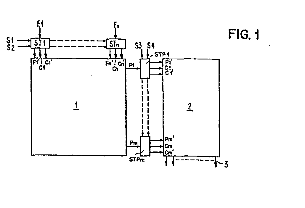
Description
Die Erfindung betrifft eine programmierbare hochintegrierte logische Schaltungsanordnung (PLA) nach dem Oberbegriff des Patentanspruchs 1.The invention relates to a programmable, highly integrated logic circuit arrangement (PLA) according to the preamble of
Derartige programmierbare hochintegrierte logische Schaltungsanordnungen sind grundsätzlich bekannt, so z.B. aus dem Buch "MOS/LSI Design and Application" von W. Carr und J. Mice, McGraw-Hill, 1972, Seiten 229 bis 258. Mit Hilfe derartiger programmierbarer logischer Schaltungsanordnungen ist die direkte Implementierung kombinatorischer Logik in regelmäßigen Strukturen, insbesondere Matrixanordnungen möglich, wodurch sich gegenüber den nicht in regelmäßigen Strukturen zusammengeschalteten logischen Verknüpfungsschaltungen der Vorteil ergibt, daß sich sowohl die Massenherstellung als auch das Testen und die Lagerhaltung wesentlich vereinfachen. Neben den programmierbaren logischen Anordnungen, deren Informationsinhalt bereits während des Herstellungsvorgangs fest eingeprägt wird und danach nicht mehr zu ändern ist, sind auch solche programmierbare logische Anordnungen bekannt geworden, die eine Programmierung auch nach dem Herstellungsprozeß erlauben. Als Beispiel für eine deratige Anordnung sei auf die US-PS 3 987 286 hingewiesen.Such programmable, highly integrated logic circuit arrangements are known in principle, e.g. from the book "MOS / LSI Design and Application" by W. Carr and J. Mice, McGraw-Hill, 1972, pages 229 to 258. With the aid of such programmable logic circuit arrangements, the direct implementation of combinatorial logic in regular structures, in particular matrix arrangements, is possible , which has the advantage over the logical logic circuits not interconnected in regular structures that mass production as well as testing and warehousing are considerably simplified. In addition to the programmable logic arrangements, the information content of which is already firmly imprinted during the manufacturing process and cannot be changed thereafter, programmable logic arrangements have also become known which permit programming even after the manufacturing process. As an example of such an arrangement, reference is made to US Pat. No. 3,987,286.
Auch Mehrfachpersonalisierungen mit besonderen Koppel- und Verknüpfungselementen sind bekannt, die mehrere Zustände einnehmen können. Hierzu wird auf das IBM TDB Vol. 17, Nr.3, August 1974, Seiten 811 und 812 verwiesen. Derartige Lösungen sind jedoch wegen der benötigten Sonderbauelemente, wegen der hohen Redundanz der Bauelemente und wegen der geringen Operationsgeschwindigkeit in der Praxis nicht eingesetzt worden.Multiple personalizations with special coupling and linking elements are also known, which can assume several states. Reference is made to the IBM TDB Vol. 17, No. 3, August 1974, pages 811 and 812. However, such solutions are because of the special components required, because of the high redundancy of the components and because of low operating speed have not been used in practice.
Aus dem IBM TDB, Vol. 20, Nr. 10, März 1978, Seiten 4016 bis 4018 und der US-PS 4 084 152 sind programmierbare logische Schaltungsanordnungen in hochintegrierter Technik bekannt geworden, bei denen verbleibende ungenutzte VerknUpfungsbereiche, d.h. redundante Schaltkreise verringert werden. Diese Schaltungsanordnungen haben jedoch den Nachteil, daß sie erhebliche Einschränkungen hinsichtlich des Freiheitsgrads, den der mit der Auslegung komplexer Verknüpfungsnetzwerke befaßte Fachmann hat, aufweisen. Damit geht der ansich erforderliche hohe Grad an Flexibilität bei regelmäßigen Strukturen wieder verloren, so daß auch der Einsatz dieser programmierbaren logischen Anordnungen in der Praxis nur äußerst beschränkt möglich ist.From IBM TDB, Vol. 20, No. 10, March 1978, pages 4016 to 4018 and US Pat. No. 4,084,152, programmable logic circuit arrangements in highly integrated technology have become known in which remaining unused link areas, i.e. redundant circuits can be reduced. However, these circuit arrangements have the disadvantage that they have considerable restrictions with regard to the degree of freedom which the person skilled in the design of complex linking networks has. As a result, the high degree of flexibility required per se in regular structures is lost again, so that the use of these programmable logic arrangements is only possible to an extremely limited extent in practice.
In der europäischen Patentanmeldung 80 106 964 ist deshalb eine weitere Verbesserung dieser programmierbaren logischen Anordnungen in hochintegrierter Technik aufgezeigt worden, die höhere Funktionsdichten sowie eine schnelle elektrische Umschaltung zwischen unterschiedlichen Funktionen erlaubt und keine hohen Umprogrammierungsspannungen oder Sonderbauelemente erfordert. Diese Anordnung ist dadurch gekennzeichnet, daß die Koppelelemente Feldeffekttransistoren mit mindestens zwei nebeneinander vorsehbaren Gate-Abschnitten sind, wobei ein Leitendwerden der zugehörigen Source-Drain-Schaltstrecke erst ermöglicht wird, wenn an mindestens den beiden Gate-Abschnitten die zugehörigen Einschaltpotentiale vorliegen, und daß diese mindestens beiden umschaltbaren Funktionen in der Weise eingeprägt werden, daß bei einer nur im Rahmen einer der beiden oder mehreren Funktionen herzustellenden Verbindung einer der Gate-Abschnitte mit der für die Funktionsauswahl maßgeblichen Steuerleitung und der mindestens eine verbleibende Gateabschnitt eines solchen Koppelelementes mit der betreffenden Eingangsleitung verbunden wird, und daß bei ihm im Rahmen der mindestens beiden Funktionen herzustellenden Verbindungen, die mindestens beiden Gate-Abschnitte eines solchen Koppelelements gemeinsam an die betreffende Eingangsleitung angeschlossen sind. Obwohl sich eine derartige Anordnung durch eine sehr gute Flächennutzung auszeichnet und deshalb für hochinte- grierte Bauweise geeignet ist, bleibt jedoch der alte Nachteil immer noch bestehen, daß der redundante Anteil von Bauelementen zu hoch ist.European patent application 80 106 964 has therefore shown a further improvement of these programmable logic arrangements in highly integrated technology, which allows higher functional densities and fast electrical switching between different functions and does not require high reprogramming voltages or special components. This arrangement is characterized in that the coupling elements are field-effect transistors with at least two gate sections which can be provided next to one another, the associated source-drain switching path only becoming conductive when the associated switch-on potentials are present on at least the two gate sections, and in that these at least two switchable functions are impressed in such a way that in the case of a connection to be established only in the context of one of the two or more functions, one of the gate sections with the control line relevant for the function selection and the at least one remaining gate section of a sol Chen coupling element is connected to the relevant input line, and that with him in the context of the at least two functions to be made connections, the at least two gate sections of such a coupling element are connected together to the relevant input line. Although such an arrangement is characterized by a very good use of space and is therefore suitable for hochinte- g rated construction, but the old drawback remains still insist that the redundant portion of components is too high.
Der Erfindung liegt deshalb die Aufgabe zugrunde, eine programmierbare logische hochintegrierte Schaltungsanordnung zu schaffen, die die Aktivierung des Don't Care-Zustands der Zellen und die gleichzeitige Inaktivierung der funktionellen PLA-Bits ermöglicht.The invention is therefore based on the object of providing a programmable logic, highly integrated circuit arrangement which enables the activation of the don't care state of the cells and the simultaneous deactivation of the functional PLA bits.
Die erfindungsgemäße Lösung ergibt sich aus dem Kennzeichen des Patentanspruchs 1. Weitere Ausgestaltungen der Erfindung sind in den Patentansprüchen 2 bis 6 charakterisiert.The solution according to the invention results from the characterizing part of
Durch die Aktivierung des Don't Care-Zustands der Zellen innerhalb der programmierbaren logischen hochintegrierten Schaltungsanordnung und durch die separate Ansteuermöglichkeit des UND- und des ODER-Bereichs der programmierbaren logischen Anordnung ist eine hohe Anzahl von logischen Funktionen bei drastischer Verringerung der Redundanz an Schaltkreisen ermöglicht worden.By activating the don't care state of the cells within the programmable logic highly integrated circuit arrangement and through the separate control possibility of the AND and OR regions of the programmable logic arrangement, a large number of logic functions is possible with a drastic reduction in the redundancy on circuits been.
Durch die eingeführte Steuerschaltung in Form einer zweistufigen UND/ODER-Schaltung ist eine elegante Ansteuerung der UND- und ODER-Bereiche ermöglicht worden, da sich eine derartige Steuerschaltung sehr gut in die gesamte Struktur der programmierbaren logischen Anordnung in hochintegrierter Technik einfügt. Der zusätzliche, für die Steuerlogik erforderliche Platzbedarf kann somit äußerst gering gehalten werden.The introduced control circuit in the form of a two-stage AND / OR circuit enables elegant control of the AND and OR areas, since such a control circuit fits very well into the entire structure of the programmable logic arrangement using highly integrated technology. The additional space required for the control logic can thus be kept extremely low.
Die Erfindung wird nun anhand von in der Zeichnung dargestellten Ausführungsbeispielen näher erläutert.The invention will now be explained in more detail with reference to exemplary embodiments shown in the drawing.
Es zeigen:
- Fig. 1 ein Blockschaltbild einer programmierbaren logischen Anordnung mit dazwischenliegenden Steuerschaltungen,
- Fig. 2 ein spezielles Ausführungsbeispiel in Feldeffekt-Transistortechnik mit zwei Gate-Elektroden pro Feldeffekttransistor,
- Fig. 3 eine Zelle einer programmierbaren logischen Anordnung mit Aktivierung des Don't Care-Zustands und
- Fig. 4 die Funktionsdarstellungsweise in einer zweifach adressierbaren programmierbaren logischen Anordnung mit drei Funktionen.
- 1 is a block diagram of a programmable logic arrangement with control circuits in between;
- 2 a special embodiment in field effect transistor technology with two gate electrodes per field effect transistor,
- Fig. 3 shows a cell of a programmable logic arrangement with activation of the don't care state and
- Fig. 4 shows the functional representation in a double addressable programmable logic arrangement with three functions.
Die in Fig. 1 dargestellte programmierbare logische Schaltungsanordnung eignet sich besonders für die Herstellung in hochintegrierter Technik, da sie sich durch eine regelmä- βige Struktur auszeichnet und die dazwischenliegenden Steuerschaltungen ebenfalls aus kombinierten UND- und ODER-Schaltungen bestehen. Aufgebaut ist diese programmierbare logische Schaltungsanordnung aus einem UND-Feld 1 und einem ODER-Feld 2, wobei dem UND-Feld 1 Schaltungen ST1 bis Stn zur Selektierung einer der möglichen Zellen vorgeschaltet sind. An jeder durch einen Block dargestellten Steuerschaltung ST1 bis STn liegen gemeinsam die Steuereingänge S1 und S2 und je ein Funktionseingang F1, F2, ... oder Fn. Die Ausgänge jeder Steuerschaltung ST1 bis Stn sind mit F1', Cl, Cl', ..., Fn', Cn, Cn' bezeichnet. Diese Schaltung zur Selektierung einer der fünf möglichen Zellen innerhalb der programmierbaren logischen Anordnung muß für jeden Funktionsstrang folgende Bedingung erfüllen:

Das UND-Feld 1 weist Produkt-Termleitungen P1 bis Pm auf, die über Steuerschaltungen STP1 bis STPm sowie deren Ausgangsleitungen P1', Cl, Cl', ... Pm', Cm, Cm' auf das ODER-Feld wirken. An den Steuerschaltungen STP1 bis STPm liegen außerdem die Steuereingänge S3 und S4. An der unteren Kante des ODER-Feldes 2 sind die Ausgänge bzw. Ausgangsleitungen 3 der programmierbaren logischen Anordnung eingezeichnet. Der Aufbau der Steuerschaltungen ST1 bis Stn und STPm wird später anhand der Fig. 2 näher erklärt.The
In der Fig. 2 ist nun ein detaillierteres Schaltbild einer programmierbaren logischen Schaltungsanordnung gezeigt, die sich besonders zur Höchstintegration durch die Verwendung von Feldeffekttransistoren mit zwei Torelektroden eignet. Bevor jedoch die Wirkungsweise näher beschrieben wird, soll zunächst der Aufbau und die Wirkungsweise einer einzelnen Zelle nach Fig. 3 beschrieben werden. Eine einzelne Zelle für die hier beschriebene programmierbare logische Schaltungsanordnung besteht aus einem Feldeffekttransistor FET. Dieser Feldeffekttransistor FET besitzt zwei Torelektroden Tl und T2. Die eine Elektrode des Feldeffekttransistors FET, vorteilhafterweise die Drainelektrode, ist über eine Leitung und einen Widerstand R mit einer Spannung V+ verbunden. Außerdem sind die senkrecht zu dieser Leitung verlaufende Leitung FKT1, 2, die Leitung C und die Leitung C' vorhanden. Die Leitung FKT1, 2 ist die bei der Zweifach-Personalisierung erforderliche Funktionsleitung, wobei für die beiden Funktionen FKT1 und FKT2 folgende Definition gilt: FKT1 :
![]()
![]()
Die entsprechenden Leitungsverbindungen zu den zwei Elektroden Tl und T2 müssen dieser Tabelle genügen. Wenn man nun den Don't Care-Zustand FKT3 aktivieren will, muß man die in Fig. 3 eingezeichneten Verbindungen zu den Torelektroden Tl und T2 des Feldeffekttransistors des FET herstellen. Diese Verbindungen genügen der folgenden logischen Tabelle zur Aktivierung:
- FKT3 = C = C'
- FKT 1, 2 = 0
- FKT3 = C = C '
- FKT 1, 2 = 0
Dieser Zustand blieb nämlich bisher bei der zweifachen Personalisierung, wie sie weiter oben beschrieben ist, ungenutzt.This condition has so far remained unused in the double personalization described above.
Im folgenden wird nun das in Fig. 2 detailliertere Schaltbild einer programmierbaren logischen Schaltungsanordnung gemäß Fig. 1 näher beschrieben. Die Darstellung gemäß Fig.2 zeigt die praktische Realisierungsmöglichkeit mit Hilfe von Zellen gemäß Fig. 3 sehr deutlich. Im oberen Teil der Fig.2 sind die Steuerschaltungen STO, ST1 und ST2 zu sehen, die mit den gemeinsamen Steuerleitungen S1 und S2 verbunden sind. An den oberen Eingangsleitungen liegen jeweils die Signale Fv0 und F0, Fvl und F1 sowie Fv2 und F2 an den entsprechenden Steuerschaltungen. Wie aus dem Aufbau der Steuerschaltungen STO zu sehen ist, bestehen die identisch aufgebauten Steuereinheiten STO, ST1 und ST2 aus UND- und ODER-Schaltungen. An den Ausgängen der Steuerschaltungen stehen die Signal C und C sowie FO und FO bei der Steuereinheit STO und bei der Steuereinheit ST1, die Signale C und C, bzw. F1 und FT zur Verfügung. An den Ausgängen der Steuerschaltung ST2 stehen die entsprechenden Signale zur Verfügung, wie aus der Fig. 2 hervorgeht. Die diese Ausgangssignale führenden Leitungen sind mit den Torelektroden der Zellen des UND-Feldes 1 spaltenweise verbunden und zwar so, daß jeder Steuerschaltung vorteilhafterweise zwei Spalten, nämlich eine mit der wahren Funktion FO und die andere mit der negierten Funktion FO zugeordnet sind. Als Ausgangsleitungen des UND-Feldes 1 dienen die waagerecht verlaufenden Leitungungen PO bis Pn, von denen jedoch nur fünf in der Fig. 2 dargestellt sind. Diese waagerecht verlaufenden Leitungen PO bis Pn sind an ihrem anderen Ende über je einen Widerstand mit einem gemeinsamen Anschlußpunkt, an dem eine Spannung +V anliegt, verbunden. Die Ausgangsenden dieser Leitungen PO bis Pn führen als Eingangsleitungen zu den zwischen dem UND-Feld 1 und dem ODER-Feld 2 liegenden Steuerschaltungen STPO bis STPn, wobei auch hier wieder nur in Fig. 2 fünf Steuerschaltungen dargestellt sind. Außerdem sind diese Steuerschaltungen STPO bis STPn mit Leitungen verbunden, auf denen die Steuersignale S3 und S4 zugeführt werden. Die Eingänge PvO... Pvm können mit beliebigen Produktterm-Leitungen (PO ... 8m) zur optimalen Ausnutzung der Don't Care-Position verbunden werden. Die Ausgangsleitungen derThe circuit diagram of a programmable logic circuit arrangement according to FIG. 1, which is detailed in FIG. 2, will now be described in more detail below. The representation according to Fig. 2 shows the practical implementation possibility with the aid of cells according to FIG. 3 very clearly. In the upper part of Figure 2, the control circuits STO, ST1 and ST2 can be seen, which are connected to the common control lines S1 and S2. The signals Fv0 and F0, Fvl and F1 and Fv2 and F2 are connected to the corresponding control circuits on the upper input lines. As can be seen from the structure of the control circuits STO, the identically constructed control units STO, ST1 and ST2 consist of AND and OR circuits. At the outputs of the control circuits, the signals C and C as well as FO and FO in the control unit STO and in the control unit ST1, the signals C and C, or F1 and FT are available. The corresponding signals are available at the outputs of the control circuit ST2, as can be seen from FIG. 2. The lines carrying these output signals are connected in columns to the gate electrodes of the cells of the AND
GE 980 046 E Steuerschaltungen STPO bis STPn sind nun ihrerseits mit den Torelektroden jeweils einer Reihe von Zellen des ODER-Feldes 2 verbunden. Die Zellen des ODER-Feldes 2 bestehen ebenfalls wieder aus einer Grundzelle gemäß Fig. 3. Senkrecht zu den Ausgangsitungen der Steuerleitungen STPO bis STPn verlaufen die Summentermleitungen 3 bzw. FKT 1, 2 ... der programmierbaren logischen Anordnung, auf denen das logische Ausgangsprodukt nach Vollendung einer Operation erscheint. Das andere Ende dieser Leitungen ist jeweils über einen Widerstand mit einer Spannungsquelle +V verbunden.GE 980 046 E Control circuits STPO to STPn are in turn connected to the gate electrodes of a row of cells of the
Die Steuerschaltungen STO, ST1 oder ST2 zur Selektierung einer der fünf möglichen Zellenzustände müssen für jeden Funktionsstrang v folgende Bedingungen erfüllen:

Diesen soeben angegebenen Funktionen entspricht die Schaltung aus UND- und ODER-Schaltungen, die in der Steuerschaltung STO gezeigt ist. Der Aufbau für die Steuerschaltungen ST1 und ST2 ist selbstverständlich analog und auch der zwischen dem UND- und dem ODER-Feld der programmierbaren logischen Anordnung angeordneten Steuerschaltungen STPO bis STPn ist analog. Zur optimalen Ausnutzung der Don't Care-Zustände einer programmierbaren logischen Schaltungsanordnung kann jeder Funktionseingang Fn auf jeden beliebigen Funktionsstrang der programmierbaren logischen Schaltungsanordnung geschaltet werden.The circuit of AND and OR circuits shown in the control circuit STO corresponds to these functions just specified. The structure for the control circuits ST1 and ST2 is of course analog and the same Control circuits STPO to STPn arranged between the AND and OR fields of the programmable logic arrangement are analogous. For optimal use of the don't care states of a programmable logic circuit arrangement, each function input Fn can be switched to any function string of the programmable logic circuit arrangement.
Im folgenden werden nun Funktionskombinationen angegeben. Durch die separate Ansteuermöglichkeit des UND- und des ODER-Feldes 1 und 2 können somit neun logische Funktionen realisiert werden. Dies geht aus der nachfolgenden Tabelle hervor.

Wie bereits ausgeführt worden ist, können die Steuerschaltungen ST1 bis n und STP1 bis n sehr gut in die Struktur der programmierbaren logischen Schaltungsanordnung, die ebenfalls aus UND- und ODER-Schaltungen besteht, integriert werden. Daraus ergibt sich ein relativ kleiner Flächenbedarf für diese Steuerschaltungen, der nicht ins Gewicht fällt. GE 980 046 E As has already been explained, the control circuits ST1 to n and STP1 to n can be integrated very well into the structure of the programmable logic circuit arrangement, which also consists of AND and OR circuits. This results in a relatively small area requirement for these control circuits, which is not significant. GE 980 046 E
Je nach Verwendung der programmierbaren logischen Schaltungen differiert die Anzahl der Eingänge, die Anzahl der Leitungen für die Produktterme und die Anzahl der Leitungen für die Summenterme. Bei solchen mit sehr vielen Produkttermen ist die Integration einer zusätzlichen Steuerleitung in das ODER-Feld 2 zu empfehlen. Dadurch reduziert sich die Steuerlogik für das gesamte ODER-Feld 2 auf zwei logische UND-Glieder. Ein weiterer Vorteil ist die dadurch mögliche Dreifachbenutzung der Bits, wodurch für die ODER-Funktion S3 somit nicht nur die Don't Care-Positionen, sondern auch die schon zweifach belegten Positionen benutzt werden können. In Fig. 4 ist nun schematisch ein Teil der programmierbaren logischen Schaltungsanordnung in personalisierter Form dargestellt. Links ist wieder in schemati--sierter Form das UND-Feld 1 und rechts das ODER-Feld 2 gezeigt. Anstelle der Steuerschaltungen STPO bis STP4 und STO bis ST2 gemäß Fig. 2 sind hier die von diesen Steuerschaltungen an die einzelnen Spaltenleitungen im UND-Feld 1 gelieferten logischen Signale eingezeichnet.Depending on the use of the programmable logic circuits, the number of inputs, the number of lines for the product terms and the number of lines for the total terms differs. For those with a large number of product terms, the integration of an additional control line in OR
F0, F1, F3 sind dabei die Eingangsoperanden. Wie aus der oberhalb der schematisch dargestellten personalisierten programmierbaren logischen Anordnung dargestellten kleinen Tabelle mit den Zuordnungssymbolen innerhalb des UND-Feldes bzw. des ODER-Feldes 1 bzs.*2 hervorgeht, entsprechen sich hier folgende Ausdrücke:
- FO entspricht AO mit dem schwarzen Dreieck bzw.
AO mit dem weißen Dreick bzw.
A mit dem gestrichelten Dreieck,
in den Kreuzungspunkten der senkrecht und waagrecht verlaufenden Leitungen. - F1 entspricht BO mit dem zugeordneten schwarzen Dreieck, bzw.
A1 mit dem zugeordneten weißen Dreieck, bzw.
B mit dem zugeordneten gestrichelten Dreieck GE 980 046E und F2 entspricht CIN mit dem schwarzen Dreieck bzw.
A2 mit dem weißen Dreieck.
- FO corresponds to AO with the black triangle or
AO with the white triangle or
A with the dashed triangle,
at the crossing points of the vertical and horizontal lines. - F1 corresponds to BO with the assigned black triangle, or
A1 with the assigned white triangle, or
B with the assigned dashed triangle GE 980 046 E and F2 corresponds to CIN with the black triangle or
A2 with the white triangle.
Fv bedeutet hier "variabler" Eingang. Für die dritte Personalisierungsebene, das sind die Zellen mit den aktivierten Don't Care-Zuständen, können Eingänge wahlweise belegt werden (z.B. F2 auf Fv der Steuerschaltung STO). Im Anwendungsbeispiel wurde davon Gebrauch gemacht.Fv here means "variable" input. For the third level of personalization, i.e. the cells with the activated don't care states, inputs can be assigned (e.g. F2 to Fv of the control circuit STO). This was used in the application example.
Im Nachfolgenden werden für die Funktionen Zweierkomplement, Volladdierer und Decoder die zu implementierenden Funktionen angegeben, wobei zunächst eine Tabelle für die Steuereingänge Sl bis S4 angegeben wird.


Das Testen der programmierbaren logischen Anordnung kann durch Selektieren der aktivierbaren Don't Care-Positionen in einer zweifach adressierbaren programmierbaren logischen Schaltungsanordnungen erfolgen, wobei folgendes Testprinzip zugrundegelegt wird:
- 1. Eindeutige Zuordnung der ersten bzw. zweiten Ebene der programmierbaren logischen Anordnung (Personalisierungsebene) des UND-
Feldes 1 zur Testebene (Don't Care-Ebene) des ODER-Feldes 2 zum Testen des UND-Feldes 1. - 2. Eindeutige Zuordnung der ersten bzw. zweiten Ebene der programmierbaren logischen Schaltungsanordnung des ODER-
Feldes 2 zur Testebene des UND-Feldes 1 zum Testen des ODER-Feldes 2.
- 1. Clear assignment of the first or second level of the programmable logical arrangement (personalization level) of the AND
field 1 to the test level (don't care level) of theOR field 2 for testing the ANDfield 1. - 2. Clear assignment of the first or second level of the programmable logic circuit arrangement of the
OR field 2 to the test level of the ANDfield 1 for testing theOR field 2.
Dadurch wird jeder Produktterm bzw. Summenterm durch die Selektierung der aktivierbaren Don't Care-Positionen in einer zweifach adressierbaren logischen Schaltungsanordnung getestet.As a result, each product term or total term is tested by selecting the activable don't care positions in a double-addressable logic circuit arrangement.
Claims (7)
Applications Claiming Priority (2)
| Application Number | Priority Date | Filing Date | Title |
|---|---|---|---|
| DE3121562 | 1981-05-30 | ||
| DE19813121562 DE3121562A1 (en) | 1981-05-30 | 1981-05-30 | PROGRAMMABLE LOGICAL HIGHLY INTEGRATED CIRCUIT ARRANGEMENT |
Publications (3)
| Publication Number | Publication Date |
|---|---|
| EP0066050A2 true EP0066050A2 (en) | 1982-12-08 |
| EP0066050A3 EP0066050A3 (en) | 1984-05-09 |
| EP0066050B1 EP0066050B1 (en) | 1987-06-24 |
Family
ID=6133576
Family Applications (1)
| Application Number | Title | Priority Date | Filing Date |
|---|---|---|---|
| EP82102403A Expired EP0066050B1 (en) | 1981-05-30 | 1982-03-23 | Large-scale integrated programmable logic array |
Country Status (4)
| Country | Link |
|---|---|
| US (1) | US4468735A (en) |
| EP (1) | EP0066050B1 (en) |
| JP (1) | JPS57203337A (en) |
| DE (2) | DE3121562A1 (en) |
Families Citing this family (5)
| Publication number | Priority date | Publication date | Assignee | Title |
|---|---|---|---|---|
| JPS61170828A (en) * | 1985-01-24 | 1986-08-01 | Hitachi Ltd | microprogram controller |
| US4858178A (en) * | 1986-09-30 | 1989-08-15 | Texas Instruments Incorporated | Programmable sequence generator |
| US4880754A (en) * | 1987-07-06 | 1989-11-14 | International Business Machines Corp. | Method for providing engineering changes to LSI PLAs |
| US8438522B1 (en) | 2008-09-24 | 2013-05-07 | Iowa State University Research Foundation, Inc. | Logic element architecture for generic logic chains in programmable devices |
| US8661394B1 (en) | 2008-09-24 | 2014-02-25 | Iowa State University Research Foundation, Inc. | Depth-optimal mapping of logic chains in reconfigurable fabrics |
Family Cites Families (11)
| Publication number | Priority date | Publication date | Assignee | Title |
|---|---|---|---|---|
| US3987286A (en) * | 1974-12-20 | 1976-10-19 | International Business Machines Corporation | Time split array logic element and method of operation |
| AT345902B (en) * | 1975-03-25 | 1978-10-10 | Siemens Ag | INTEGRATED COMPONENTS WITH MULTIPLE LINKING LINKS FOR DIFFERENT LINK FUNCTIONS |
| US4084152A (en) * | 1976-06-30 | 1978-04-11 | International Business Machines Corporation | Time shared programmable logic array |
| US4103182A (en) * | 1976-09-01 | 1978-07-25 | Hewlett-Packard Company | Programmable transfer gate array |
| FR2396468A1 (en) * | 1977-06-30 | 1979-01-26 | Ibm France | IMPROVEMENT IN PROGRAMMABLE LOGIC NETWORKS |
| US4195352A (en) * | 1977-07-08 | 1980-03-25 | Xerox Corporation | Split programmable logic array |
| US4177452A (en) * | 1978-06-05 | 1979-12-04 | International Business Machines Corporation | Electrically programmable logic array |
| US4233667A (en) * | 1978-10-23 | 1980-11-11 | International Business Machines Corporation | Demand powered programmable logic array |
| US4293783A (en) * | 1978-11-01 | 1981-10-06 | Massachusetts Institute Of Technology | Storage/logic array |
| US4208728A (en) * | 1978-12-21 | 1980-06-17 | Bell Telephone Laboratories, Incorporated | Programable logic array |
| US4354228A (en) * | 1979-12-20 | 1982-10-12 | International Business Machines Corporation | Flexible processor on a single semiconductor substrate using a plurality of arrays |
-
1981
- 1981-05-30 DE DE19813121562 patent/DE3121562A1/en not_active Withdrawn
-
1982
- 1982-03-23 EP EP82102403A patent/EP0066050B1/en not_active Expired
- 1982-03-23 DE DE8282102403T patent/DE3276650D1/en not_active Expired
- 1982-04-02 JP JP57053935A patent/JPS57203337A/en active Granted
- 1982-05-17 US US06/378,959 patent/US4468735A/en not_active Expired - Lifetime
Also Published As
| Publication number | Publication date |
|---|---|
| DE3121562A1 (en) | 1983-01-05 |
| DE3276650D1 (en) | 1987-07-30 |
| JPH0211179B2 (en) | 1990-03-13 |
| EP0066050A3 (en) | 1984-05-09 |
| JPS57203337A (en) | 1982-12-13 |
| US4468735A (en) | 1984-08-28 |
| EP0066050B1 (en) | 1987-06-24 |
Similar Documents
| Publication | Publication Date | Title |
|---|---|---|
| EP0051693B1 (en) | Electrically switchable read-only memory | |
| DE2723821C2 (en) | Programmable logical arrangement | |
| DE69528393T2 (en) | Programmable logic module for a user-programmable gate array | |
| DE2434704C2 (en) | Programmable link matrix | |
| DE69122065T2 (en) | Programmable integrated circuit | |
| DE102004014472B4 (en) | Application specific semiconductor integrated circuit | |
| DE2556274C2 (en) | Programmable logic circuit | |
| DE69132984T2 (en) | Programmable connection architecture | |
| DE3712178C2 (en) | ||
| DE69325133T2 (en) | Semiconductor read-only memory | |
| DE2556275A1 (en) | HIGH DENSITY LOGICAL CIRCUIT | |
| DE19519794A1 (en) | Holding circuit for semiconductor substrate integrated data processor | |
| EP0280176A1 (en) | Basic cell for a gate array | |
| DE69018832T2 (en) | EEPROM cell with a single-layer metal gate and with a read interface of the external circuit, which is isolated from the write / erase interface of the programming circuit. | |
| DE2261786C3 (en) | ||
| DE2261786B2 (en) | Fixed-value storage unit | |
| DE2514012C2 (en) | MONOLITHICALLY INTEGRATED SEMICONDUCTOR CIRCUIT ARRANGEMENT, IN PARTICULAR FOR COUPLING COMPONENTS OF SWITCHING SYSTEMS | |
| DE2828325A1 (en) | EMITTER COUPLED LOGIC STAGE | |
| EP0061513B1 (en) | Cmos integrated selection circuit for four potentials and simplifications of it for three potentials | |
| EP0348539A1 (en) | Programmable CMOS logic array | |
| EP0166027B1 (en) | C-mos basic cell | |
| EP0066050B1 (en) | Large-scale integrated programmable logic array | |
| DE2525690C3 (en) | Logical DOT connection circuit in complementary field effect transistor technology | |
| DE2855342C2 (en) | Memory circuit | |
| DE4327290A1 (en) | Master-slice type integrated circuit - has several semiconductor regions which are mutually insulated, set in first longitudinal direction, and connected to several supply lines |
Legal Events
| Date | Code | Title | Description |
|---|---|---|---|
| PUAI | Public reference made under article 153(3) epc to a published international application that has entered the european phase |
Free format text: ORIGINAL CODE: 0009012 |
|
| AK | Designated contracting states |
Designated state(s): DE FR GB |
|
| 17P | Request for examination filed |
Effective date: 19830322 |
|
| PUAL | Search report despatched |
Free format text: ORIGINAL CODE: 0009013 |
|
| AK | Designated contracting states |
Designated state(s): DE FR GB |
|
| GRAA | (expected) grant |
Free format text: ORIGINAL CODE: 0009210 |
|
| AK | Designated contracting states |
Kind code of ref document: B1 Designated state(s): DE FR GB |
|
| ET | Fr: translation filed | ||
| REF | Corresponds to: |
Ref document number: 3276650 Country of ref document: DE Date of ref document: 19870730 |
|
| PLBE | No opposition filed within time limit |
Free format text: ORIGINAL CODE: 0009261 |
|
| STAA | Information on the status of an ep patent application or granted ep patent |
Free format text: STATUS: NO OPPOSITION FILED WITHIN TIME LIMIT |
|
| 26N | No opposition filed | ||
| PGFP | Annual fee paid to national office [announced via postgrant information from national office to epo] |
Ref country code: GB Payment date: 19920210 Year of fee payment: 11 |
|
| PGFP | Annual fee paid to national office [announced via postgrant information from national office to epo] |
Ref country code: DE Payment date: 19920321 Year of fee payment: 11 |
|
| PGFP | Annual fee paid to national office [announced via postgrant information from national office to epo] |
Ref country code: FR Payment date: 19930226 Year of fee payment: 12 |
|
| PG25 | Lapsed in a contracting state [announced via postgrant information from national office to epo] |
Ref country code: GB Effective date: 19930323 |
|
| GBPC | Gb: european patent ceased through non-payment of renewal fee |
Effective date: 19930323 |
|
| PG25 | Lapsed in a contracting state [announced via postgrant information from national office to epo] |
Ref country code: DE Effective date: 19931201 |
|
| PG25 | Lapsed in a contracting state [announced via postgrant information from national office to epo] |
Ref country code: FR Effective date: 19941130 |
|
| REG | Reference to a national code |
Ref country code: FR Ref legal event code: ST |