EP0066053B1 - Dispositif et procédé pour l'exposition à la lumière d'un milieu photosensible - Google Patents
Dispositif et procédé pour l'exposition à la lumière d'un milieu photosensible Download PDFInfo
- Publication number
- EP0066053B1 EP0066053B1 EP19820102516 EP82102516A EP0066053B1 EP 0066053 B1 EP0066053 B1 EP 0066053B1 EP 19820102516 EP19820102516 EP 19820102516 EP 82102516 A EP82102516 A EP 82102516A EP 0066053 B1 EP0066053 B1 EP 0066053B1
- Authority
- EP
- European Patent Office
- Prior art keywords
- raman
- medium
- excimer laser
- light
- laser
- Prior art date
- Legal status (The legal status is an assumption and is not a legal conclusion. Google has not performed a legal analysis and makes no representation as to the accuracy of the status listed.)
- Expired
Links
Images



Classifications
-
- G—PHYSICS
- G03—PHOTOGRAPHY; CINEMATOGRAPHY; ANALOGOUS TECHNIQUES USING WAVES OTHER THAN OPTICAL WAVES; ELECTROGRAPHY; HOLOGRAPHY
- G03F—PHOTOMECHANICAL PRODUCTION OF TEXTURED OR PATTERNED SURFACES, e.g. FOR PRINTING, FOR PROCESSING OF SEMICONDUCTOR DEVICES; MATERIALS THEREFOR; ORIGINALS THEREFOR; APPARATUS SPECIALLY ADAPTED THEREFOR
- G03F7/00—Photomechanical, e.g. photolithographic, production of textured or patterned surfaces, e.g. printing surfaces; Materials therefor, e.g. comprising photoresists; Apparatus specially adapted therefor
- G03F7/70—Microphotolithographic exposure; Apparatus therefor
- G03F7/70483—Information management; Active and passive control; Testing; Wafer monitoring, e.g. pattern monitoring
- G03F7/7055—Exposure light control in all parts of the microlithographic apparatus, e.g. pulse length control or light interruption
- G03F7/70575—Wavelength control, e.g. control of bandwidth, multiple wavelength, selection of wavelength or matching of optical components to wavelength
-
- G—PHYSICS
- G03—PHOTOGRAPHY; CINEMATOGRAPHY; ANALOGOUS TECHNIQUES USING WAVES OTHER THAN OPTICAL WAVES; ELECTROGRAPHY; HOLOGRAPHY
- G03F—PHOTOMECHANICAL PRODUCTION OF TEXTURED OR PATTERNED SURFACES, e.g. FOR PRINTING, FOR PROCESSING OF SEMICONDUCTOR DEVICES; MATERIALS THEREFOR; ORIGINALS THEREFOR; APPARATUS SPECIALLY ADAPTED THEREFOR
- G03F7/00—Photomechanical, e.g. photolithographic, production of textured or patterned surfaces, e.g. printing surfaces; Materials therefor, e.g. comprising photoresists; Apparatus specially adapted therefor
- G03F7/70—Microphotolithographic exposure; Apparatus therefor
- G03F7/70483—Information management; Active and passive control; Testing; Wafer monitoring, e.g. pattern monitoring
- G03F7/7055—Exposure light control in all parts of the microlithographic apparatus, e.g. pulse length control or light interruption
- G03F7/70583—Speckle reduction, e.g. coherence control or amplitude/wavefront splitting
-
- H—ELECTRICITY
- H01—ELECTRIC ELEMENTS
- H01S—DEVICES USING THE PROCESS OF LIGHT AMPLIFICATION BY STIMULATED EMISSION OF RADIATION [LASER] TO AMPLIFY OR GENERATE LIGHT; DEVICES USING STIMULATED EMISSION OF ELECTROMAGNETIC RADIATION IN WAVE RANGES OTHER THAN OPTICAL
- H01S3/00—Lasers, i.e. devices using stimulated emission of electromagnetic radiation in the infrared, visible or ultraviolet wave range
- H01S3/30—Lasers, i.e. devices using stimulated emission of electromagnetic radiation in the infrared, visible or ultraviolet wave range using scattering effects, e.g. stimulated Brillouin or Raman effects
Definitions
- This invention relates to apparatus for exposing a photosensitive medium to light at a plurality of different wavelengths and to a method of exposing a photosensitive medium having a known wavelength sensitivity band.
- lasers generally produce an intense output
- lasers are known in the prior art which produce outputs in the deep UV spectral region.
- the use of lasers in projection photolithography has traditionally been considered unattractive due to the spatial and temporal coherence characteristics of most lasers.
- the invention as claimed seeks to solve the problem of producing a uniform exposure pattern at very fine resolution in an exposure time substantially faster than prior art systems.
- an apparatus for exposing a photosensitive medium to light at a plurality of different wavelengths to produce an exposed pattern on the element the apparatus being characterised by comprising a light source consisting of a pulsed rare gas halide excimer laser.
- a method of exposing a photosensitive medium having a known wavelength sensitivity band comprising the steps of:
- Our method and apparatus has the advantage of providing high resolution exposure by a pulsed laser source which has sufficient power to require very short exposure times in the range of a few seconds which, in the deep UV region, represents an improvement by about two orders of magnitude over a conventional mercury lamp.
- the excimer laser can be used in both the contact (including proximity) exposure mode and the projection exposure mode (including full-wafer scanning and step-and-repeat systems).
- the factor that makes the excimer laser usable in these systems without producing speckle is the fact that the mode structure of an excimer laser beam is not a spatially coherent single transverse mode. Instead, the beam is highly multi-mode, and can be thought of as random super-position of a large number of independent Gaussian beams.
- a further advantage of our method and apparatus is that the output wavelengths can be shifted as desired by selecting of the excimer and by the stimulated Raman scattering which can be used to produce one or more wavelengths in a desired spectral region. Therefore, the exposure wavelengths can be optimized for the photosensitive medium, rather than the other way around.
- the contact or proximity optical lithography apparatus shown schematically in Figure 1 comprises a suitable light source 10 which produces light of suitable wavelength and intensity and a suitable optical system 12 position to receive the light from source 10, to transform the light to the desired configuration, and to direct the light through a suitable mask member 14 to expose a photosensitive element 16.
- the optical system 12 includes a condensing element and optical means to direct the beam and to make the beam uniform over the area of mask member 14. The design of such optical systems 12 is well-known in the prior art so the optical system will not be described in any greater detail here.
- the mask member 14 comprises a pattern of contrast elements (opaque and transparent regions, for example) that define the pattern to be reproduced.
- Photosensitive element 16 comprises material which is sensitive to the wavelength of light from light source 10 to produce an image of the mask member pattern where exposed.
- photosensitive element 16 comprises a semiconductor wafer on which a thin coating of a photosensitive resist is added. Exposure of the resist and subsequent processing is utilized to produce predetermined patterns by processing the semiconductor wafer to generate desired semiconductor devices.
- the projection embodiment of the optical lithography system shown in Figure 2 comprises a suitable light source 20 whose function is to provide light of suitable wavelength and intensity.
- Optical system 22 functions to receive the light and, utilizing suitable condensing elements and optical elements, to uniformly illuminate the field encompassed by slit exposure member 24.
- Light from slit exposure member 24 is directed through mask member 26 to projection optical means 28.
- Projection optical means 28 is designed to direct light from slit exposure member 24 which has passed through mask member 26 to a corresponding point on photosensitive element 29.
- Mask member 26 and photosensitive element 29 are moved in synchronism (by means not shown) as shown by arrows 25, 27 as the successive areas are exposed.
- Projection optical means 28, in the embodiment shown, comprises a reflective system, but it will be recognized by those skilled in the art that the projection optical system could as well be a refractive system or a system which includes both reflective and refractive optical elements.
- FIG. 3 An alternative embodiment of a projection optical lithography system is shown in Figure 3.
- This system comprises a suitable light source 50 whose function is to provide light of suitable wavelength and intensity.
- Light from source 50 is directed to optical system 52 which utilizes suitable condensing elements and other optical elements to uniformly illuminate the field encompassed by mask member 54.
- optical system 52 The design of optical system 52 is well known in the prior art, so this optical system will not be described in any greater detail here.
- Light from optical system 52 is directed through mask member 54 to projection optical means 56.
- Projection optical means 56 is designed to produce an image (usually reduced in size) of mask member 54 on photosensitive element 58 in exposure area A.
- photosensitive element 58 comprises a semiconductor wafer having a thin coating of photosensitive resist.
- Suitable semiconductor materials include silicon, gallium arsenide, and garnets, such as gadolinium gallium garnet.
- an excimer laser light source For projection lithographic systems utilizing refractive optical elements, an excimer laser light source has an additional advantage because of its narrow bandwidth. This factor makes it simpler to correct for chromatic aberrations in the design of refractive optical elements in the projection lithographic systems. This advantage is especially significant for the design of refractive optical elements at short wavelengths where only a limited number of transparent optical materials with differing refractive indices, as required for correction of chromatic abberrations, are available.
- the light source 10 in Figure 1, 20 in Figure 2, and 50 in Figure 3 comprises rare gas halide excimer laser means 60 ( Figure 5).
- Rare gas halide excimer lasers are very efficient and powerful pulsed lasers that have only recently become commercially available. These excimer lasers emit several characteristic wavelengths from below 200 nm to above 400 nm, depending on the laser medium, and some of these are listed in Table I.
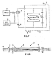
- an excimer laser is shown in Figure 7 which comprises a laser chamber 30 defined by a suitable envelope (shown by dashed line in the drawing) which confines a suitable pressurized gaseous lasing medium.
- This lasing medium may be one of those excimers shown in Table I, and this medium can be selected to provide the desired output wavelength to which the photosensitive element to be used is sensitive.
- a reservoir (not shown) is normally provided to hold a quantity of the excimer gas.
- a means (not shown) to circulate the gas to gas input pipe 38, maintain the required gas pressure within laser chamber 30, and exhaust the gas at gas outlet pipe 39 for return to the reservoir.
- Trigger circuit 34 is utilized to control the operation of the excimer laser by producing a trigger pulse at the time the laser is to be turned ON. The trigger pulse is coupled to the trigger electrode of spark gap 37, and the trigger pulse is of sufficient amplitude to cause breakdown in spark gap 37.
- spark gap 37 completes the circuit which includes the storage capacitor 36, the main electrodes 31, 32, and the preionizing spark gap 33 in parallel. This causes the gap across the main electrodes and the preionizing gap to break down. The breakdown of the main gap produces emission at the wavelength determined by the selected excimer medium, and the preionizing spark helps to make the emission more uniform.
- the large family of molecules known as excimers are characterized by a bound excited state and an unstable or very weakly bound ground state.
- a subset of excimer lasers, known as rare gas halide (RGH) lasers will be used as an example in explaining the operation of an excimer laser.
- the RGH lasers lase on transitions of molecules of the type RX, where R and X denote a rare gas atom and a halogen atom, respectively.
- Typical potential energy curves for an RGH molecule are shown in Figure 9. Population inversion is readily produced because the lower level dissociation time (-10- 11 sec) is much less than the upper level radiative lifetime (10- 9- 10- B sec).
- the excitation to the upper state (RX) * can be produced by several mechanisms.
- the excited state is the same as the ion pair R + X - , recombination of the positive rare gas ion and the negative halogen ion populates the upper level.
- the positive and negative ions are readily produced by high-energy electron collisions.
- an excited rare gas atom (R * ) can directly react with a halogen molecule.
- Yet another way of producing the upper laser state is a reaction between R * and a halogen compound, e.g., NF 3 .
- Excimer lasers can produce an average power of several watts at a number of wavelengths. With discharge-pumped systems, the obtainable pulsewidths are typically -10-100 ns. Thus, the peak powers are on the order of -10 7 W. For systems with average power in the several-watt range, the available repetition rates vary from single pulse to >1 kHz.
- the high brightness of the excimer laser light source can either be used to obtain extremely fast exposures, as was stated above, or one can use significantly smaller numerical apertures (NA) in the projection optical means of the lithographic system and still maintain reasonable exposure times. A smaller NA results in a larger depth of field, which increases quadratically with the inverse of NA. A larger depth of field permits larger tolerances in wafer distortion and focus which leads to better lithographic patterns.
- the high power output and the directionality of the excimer laser light source also permits adjustment of the NA of the-condenser optics in the lithographic system. This enables one to optimize the modulation transfer function (MTF) of the system and thus produce image patterns with the desired wall profiles in the photoresist. Both of these optimization techniques result in increased device yield in semiconductor integrated circuit fabrication.
- the excimer laser output cross-section depends upon the electrode geometry, and thus can be optimized over a wide range, depending upon the application.
- Commercial units are available which have various rectangular beam shapes, e.g., 7 mmx20 mm and 25 mmx30 mm.
- the intensity uniformity across a major portion W of the beam is excellent, as shown in Figure 10. This uniformity arises because the mode structure of these transversely excited beams is extremely non-Gaussian; in fact, it is so highly multi-mode and random that, as was stated above, interference effects due to spatial coherence in a transverse plane were nonexistent in our optical lithography apparatus.
- the wide, uniform beam of the excimer laser as contrasted to the extremely narrow and Gaussian (single transverse mode) beam of most other lasers, enables the former system to be used to produce speckle-free patterns in either a contact lithographic system or a projection lithographic system.
- the excimer gas selected for use in the excimer laser may comprise only one gas, in which case the output is at the wavelength characteristic of that excimer gas.
- the XeCI gas produces an output at 308 nm and this output provides a good match to several photoresists, such as Shipley AZ 2400 (Registered Trade Mark, for example.
- the KrF gas produces an output at 249 nm which is suitable for exposing photoresists comprising a novolak resin sensitized with a diazo ketone, such as Shipley AZ 2400 and Meldrums diazo photoresists.
- the KrCI gas produces an output at 222 nm which provides an output appropriate for materials such as the spectral characteristics of poly(methyl methacrylate) (PMMA) and poly(methyl isopropenyl ketone) (PMIPK) photoresists.
- PMMA poly(methyl methacrylate)
- PMIPK poly(methyl isopropenyl ketone)
- the use of multiple wavelengths for exposure helps to minimize the often encountered problem of standing waves in the photoresist which result from the interference between the incident exposure radiation and that reflected from the interfaces between the photosensitive medium, the substrate, and the different underlying layers that may be present.
- the multiple wavelength exposure helps to average any standing waves present so that higher resolution patterns are produced.
- one or more additional wavelengths can be produced by stimulated Raman scattering which can be used to produce one or more wavelength outputs any where within a desired spectral region.
- a light source which produces a plurality of different wavelength outputs is shown in Figure 6.
- the light source comprises excimer laser means 60 which produces an output beam 40 having at least one wavelength which is determined by the excimer gas selected for excimer laser means 60.
- the output beam 40 from the excimer laser means 60 ( Figure 6) is directed through suitable focusing optical means 41 ( Figure 8) to Raman cell 42.
- At least one secondary wavelength is produced in the output beam 49 from Raman cell 42 which is directed to expose the photosensitive medium.
- a Raman cell 42 ( Figure 8) comprises a tubular member 45 which is closed at each end by a window member 43, 44 to form an enclosure which is filled with a suitable gaseous medium.
- the Raman cell utilizes the Raman effect, the inelastic scattering process of photons by excitations in matter.
- spontaneous Raman scattering is the process by which the radiation incident on a material experiences a frequency shift due to inelastic scattering from certain characteristic excitations, e.g., molecular vibrations of the medium.
- the incident power is made large enough, this frequency-shifted scattered radiation can be stimulated.
- the conversion yield in the spontaneous Raman effect is typically -10- 7 , it can be as large as 70% in the stimulated case.
- intense coherent light can be produced at different wavelengths by stimulated Raman scattering.
- the scattered wavelengths can be both up (Stokes)- and down (anti-Stokes)-shifted from the incident laser wavelength by multiples of a molecular vibration (or other elementary excitation) characteristic of the Raman medium. Since very high peak powers are available from excimer lasers, they are ideally suited for stimulated Raman shifting. Thus, each of the wavelengths listed in Table I can be shifted to several new wavelengths by selecting different Raman media. As an example, a wide variety of wavelengths can be produced from the lasers listed in Table I by stimulated Raman scattering in H 2 , D 2 , CH 4 and liquid nitrogen. A representative group of the wavelengths that can be produced by stimulated Raman scattering is shown in Table II.
- the distribution of the incident laser pulse energy into various modes can be tailored by adjusting the gas pressure within the Raman cell and/or the optics, such as focusing optics 41.
- dichroic mirrors 47, 48 can be used.
- a further variation of the secondary wavelengths available for exposure of a photosensitive element can be produced by including two separate Raman media within the Raman cell.
- the excimer KrCI is selected and both H 2 and D 2 are included in the Raman cell.
- the advantages in utilizing multiple wavelengths in producing higher resolution patterns has been discussed above.
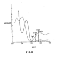
- FIG. 11 Shown in Figure 11 are the UV spectra of a photoresist material comprising a diazonaphthoquinone sensitizer (broken line spectrum) and a novolak resin (full line spectrum).
- This material is ideally suited for exposure by the 365 nm or the 405 nm line of a mercury arc lamp.
- Table I suppose a XeCl laser is available, which produces a fundamental output at 308 nm.
- the sensitizer does have absorbance at 308 nm, albeit small compared to the absorbance at slightly longer wavelengths.
Landscapes
- Physics & Mathematics (AREA)
- General Physics & Mathematics (AREA)
- Electromagnetism (AREA)
- Engineering & Computer Science (AREA)
- Plasma & Fusion (AREA)
- Optics & Photonics (AREA)
- Exposure Of Semiconductors, Excluding Electron Or Ion Beam Exposure (AREA)
- Exposure And Positioning Against Photoresist Photosensitive Materials (AREA)
- Lasers (AREA)
Claims (10)
Applications Claiming Priority (2)
| Application Number | Priority Date | Filing Date | Title |
|---|---|---|---|
| US26851181A | 1981-05-29 | 1981-05-29 | |
| US268511 | 1981-05-29 |
Publications (2)
| Publication Number | Publication Date |
|---|---|
| EP0066053A1 EP0066053A1 (fr) | 1982-12-08 |
| EP0066053B1 true EP0066053B1 (fr) | 1985-07-17 |
Family
ID=23023337
Family Applications (1)
| Application Number | Title | Priority Date | Filing Date |
|---|---|---|---|
| EP19820102516 Expired EP0066053B1 (fr) | 1981-05-29 | 1982-03-25 | Dispositif et procédé pour l'exposition à la lumière d'un milieu photosensible |
Country Status (6)
| Country | Link |
|---|---|
| EP (1) | EP0066053B1 (fr) |
| JP (1) | JPS57198631A (fr) |
| AU (1) | AU551589B2 (fr) |
| CA (1) | CA1173889A (fr) |
| DE (1) | DE3264735D1 (fr) |
| ES (1) | ES8304673A1 (fr) |
Families Citing this family (25)
| Publication number | Priority date | Publication date | Assignee | Title |
|---|---|---|---|---|
| US4417948A (en) * | 1982-07-09 | 1983-11-29 | International Business Machines Corporation | Self developing, photoetching of polyesters by far UV radiation |
| DE3376889D1 (en) * | 1982-10-07 | 1988-07-07 | Ibm | A method for etching polyimides |
| US4414059A (en) * | 1982-12-09 | 1983-11-08 | International Business Machines Corporation | Far UV patterning of resist materials |
| GB2153543B (en) * | 1983-12-28 | 1988-09-01 | Canon Kk | A projection exposure apparatus |
| JPH0695495B2 (ja) * | 1984-11-28 | 1994-11-24 | キヤノン株式会社 | 回路製造方法及びそれを用いた露光装置 |
| US5171965A (en) * | 1984-02-01 | 1992-12-15 | Canon Kabushiki Kaisha | Exposure method and apparatus |
| US5091744A (en) * | 1984-02-13 | 1992-02-25 | Canon Kabushiki Kaisha | Illumination optical system |
| GB2155650B (en) * | 1984-02-14 | 1988-11-16 | Canon Kk | Method and apparatus for exposure |
| US4773750A (en) * | 1984-06-21 | 1988-09-27 | Bruning John H | Deep-UV lithography |
| DE3588012T2 (de) * | 1984-06-21 | 1995-09-14 | At & T Corp., New York, N.Y. | Lithographie im fernen UV-Gebiet. |
| EP0293823B1 (fr) * | 1984-06-21 | 1995-04-19 | AT&T Corp. | Lithographie à rayons ultraviolets profonds |
| JPH0430052Y2 (fr) * | 1985-06-10 | 1992-07-21 | ||
| JP2600133B2 (ja) * | 1986-03-13 | 1997-04-16 | ブラザー工業株式会社 | 画像記録装置 |
| JPS63110722A (ja) * | 1986-10-29 | 1988-05-16 | Hitachi Ltd | 露光照明装置 |
| DE3750174T2 (de) * | 1986-10-30 | 1994-11-17 | Canon K.K., Tokio/Tokyo | Belichtungseinrichtung. |
| JPH0628227B2 (ja) * | 1987-10-06 | 1994-04-13 | 株式会社日立製作所 | 半導体露光装置 |
| US5310624A (en) * | 1988-01-29 | 1994-05-10 | Massachusetts Institute Of Technology | Integrated circuit micro-fabrication using dry lithographic processes |
| WO1989007285A1 (fr) * | 1988-01-29 | 1989-08-10 | Massachusetts Institute Of Technology | Micro-fabrication de circuits integres mettant en oeuvre des procedes lithographiques a sec |
| JPH021904A (ja) * | 1988-06-10 | 1990-01-08 | Mitsubishi Electric Corp | マスクの露光方法 |
| JP2858757B2 (ja) * | 1988-09-12 | 1999-02-17 | ソニー株式会社 | 配線形成法 |
| US5003567A (en) * | 1989-02-09 | 1991-03-26 | Hawryluk Andrew M | Soft x-ray reduction camera for submicron lithography |
| GB2309088A (en) * | 1996-01-12 | 1997-07-16 | Synectix Ltd | Image exposing apparatus |
| US6522386B1 (en) | 1997-07-24 | 2003-02-18 | Nikon Corporation | Exposure apparatus having projection optical system with aberration correction element |
| US6585692B1 (en) | 1999-02-19 | 2003-07-01 | Alsius Corporation | Method and system for patient temperature management and central venous access |
| US10451890B2 (en) * | 2017-01-16 | 2019-10-22 | Cymer, Llc | Reducing speckle in an excimer light source |
Family Cites Families (6)
| Publication number | Priority date | Publication date | Assignee | Title |
|---|---|---|---|---|
| GB1138084A (en) * | 1966-07-22 | 1968-12-27 | Standard Telephones Cables Ltd | Method of vapour depositing a material in the form of a pattern |
| NL7002789A (fr) * | 1969-03-01 | 1970-09-03 | ||
| DE2161743C3 (de) * | 1971-12-13 | 1974-10-10 | Fa. Carl Zeiss, 7920 Heidenheim | Vorrichtung zur stimulierten Emission von kohärenter durchstimm barer Ramanstrahlung |
| US4203078A (en) * | 1977-05-06 | 1980-05-13 | Avco Everett Research Laboratory, Inc. | Apparatus for and method of operating electron beam attachment stabilized devices for producing controlled discharges and/or visible and UV laser output |
| DE2861391D1 (en) * | 1977-12-23 | 1982-01-28 | Battelle Memorial Institute | Electrically excited impulse laser having an active gas medium |
| US4230994A (en) * | 1978-05-31 | 1980-10-28 | The United States Of America As Represented By The United States Department Of Energy | Pulse circuit apparatus for gas discharge laser |
-
1982
- 1982-01-20 JP JP57006190A patent/JPS57198631A/ja active Granted
- 1982-03-23 CA CA000399143A patent/CA1173889A/fr not_active Expired
- 1982-03-25 AU AU81898/82A patent/AU551589B2/en not_active Ceased
- 1982-03-25 EP EP19820102516 patent/EP0066053B1/fr not_active Expired
- 1982-03-25 DE DE8282102516T patent/DE3264735D1/de not_active Expired
- 1982-05-21 ES ES512422A patent/ES8304673A1/es not_active Expired
Also Published As
| Publication number | Publication date |
|---|---|
| EP0066053A1 (fr) | 1982-12-08 |
| ES512422A0 (es) | 1983-03-01 |
| AU8189882A (en) | 1982-12-02 |
| CA1173889A (fr) | 1984-09-04 |
| ES8304673A1 (es) | 1983-03-01 |
| DE3264735D1 (en) | 1985-08-22 |
| JPH0313733B2 (fr) | 1991-02-25 |
| JPS57198631A (en) | 1982-12-06 |
| AU551589B2 (en) | 1986-05-08 |
Similar Documents
| Publication | Publication Date | Title |
|---|---|---|
| US4458994A (en) | High resolution optical lithography method and apparatus having excimer laser light source and stimulated Raman shifting | |
| EP0066053A1 (fr) | Dispositif et procédé pour l'exposition à la lumière d'un milieu photosensible | |
| Jain et al. | Ultrafast high-resolution contact lithography with excimer lasers | |
| US20080165337A1 (en) | Laser system | |
| KR100505081B1 (ko) | 노광용 에이알에프 엑시머 레이저 장치 | |
| US3573456A (en) | High resolution projection means for printing micro circuits on photoresist material | |
| Silfvast | Intense EUV incoherent plasma sources for EUV lithography and other applications | |
| US6549608B1 (en) | Semiconductor manufacturing apparatus and semiconductor device manufacturing method | |
| KR100702845B1 (ko) | 엑시머 레이저 및 그의 협대역 모듈 | |
| US20050058172A1 (en) | System and method for segmented electrode with temporal voltage shifting | |
| JPH04167419A (ja) | レーザ露光装置 | |
| JP3755577B2 (ja) | 露光用ArF、KrFエキシマレーザ装置及びフッ素レーザ装置 | |
| US6885015B2 (en) | Thermionic-cathode for pre-ionization of an extreme ultraviolet (EUV) source supply | |
| US6295123B1 (en) | Multiple photon absorption for high resolution lithography | |
| US6754247B2 (en) | ArF excimer laser devices, KrF excimer laser devices and fluorine alser devices | |
| Mizoguchi et al. | Excimer Lasers for Lithography and Annealing | |
| Das et al. | Advances in excimer laser technology for sub-0.25-/spl mu/m lithography | |
| US6650678B1 (en) | Laser oscillating apparatus | |
| US20040047384A1 (en) | Gas laser apparatus for lithography | |
| CN113841309B (zh) | 生成多个激光束的设备和方法 | |
| EP1039595B1 (fr) | Laser à gaz | |
| JP4023579B2 (ja) | ArFエキシマレーザのレーザガス、ArFエキシマレーザ及びスキャン式露光機 | |
| JP2975159B2 (ja) | フォトリソグラフィー | |
| Sengupta et al. | Parametric studies and the operating latitude of a spectrally narrowed KrF excimer laser for the deep-UV stepper | |
| PETELIN et al. | Plasma sources for deep-UV lithography |
Legal Events
| Date | Code | Title | Description |
|---|---|---|---|
| PUAI | Public reference made under article 153(3) epc to a published international application that has entered the european phase |
Free format text: ORIGINAL CODE: 0009012 |
|
| AK | Designated contracting states |
Designated state(s): BE CH DE FR GB IT NL SE |
|
| 17P | Request for examination filed |
Effective date: 19830322 |
|
| ITF | It: translation for a ep patent filed | ||
| GRAA | (expected) grant |
Free format text: ORIGINAL CODE: 0009210 |
|
| AK | Designated contracting states |
Designated state(s): BE CH DE FR GB IT LI NL SE |
|
| REF | Corresponds to: |
Ref document number: 3264735 Country of ref document: DE Date of ref document: 19850822 |
|
| ET | Fr: translation filed | ||
| PLBE | No opposition filed within time limit |
Free format text: ORIGINAL CODE: 0009261 |
|
| STAA | Information on the status of an ep patent application or granted ep patent |
Free format text: STATUS: NO OPPOSITION FILED WITHIN TIME LIMIT |
|
| 26N | No opposition filed | ||
| ITTA | It: last paid annual fee | ||
| PGFP | Annual fee paid to national office [announced via postgrant information from national office to epo] |
Ref country code: BE Payment date: 19941221 Year of fee payment: 14 |
|
| EAL | Se: european patent in force in sweden |
Ref document number: 82102516.0 |
|
| PGFP | Annual fee paid to national office [announced via postgrant information from national office to epo] |
Ref country code: CH Payment date: 19950622 Year of fee payment: 14 |
|
| PGFP | Annual fee paid to national office [announced via postgrant information from national office to epo] |
Ref country code: SE Payment date: 19960307 Year of fee payment: 15 |
|
| PGFP | Annual fee paid to national office [announced via postgrant information from national office to epo] |
Ref country code: NL Payment date: 19960329 Year of fee payment: 15 |
|
| PG25 | Lapsed in a contracting state [announced via postgrant information from national office to epo] |
Ref country code: LI Effective date: 19960331 Ref country code: CH Effective date: 19960331 Ref country code: BE Effective date: 19960331 |
|
| BERE | Be: lapsed |
Owner name: INTERNATIONAL BUSINESS MACHINES CORP. Effective date: 19960331 |
|
| REG | Reference to a national code |
Ref country code: CH Ref legal event code: PL |
|
| PGFP | Annual fee paid to national office [announced via postgrant information from national office to epo] |
Ref country code: FR Payment date: 19970304 Year of fee payment: 16 |
|
| PG25 | Lapsed in a contracting state [announced via postgrant information from national office to epo] |
Ref country code: SE Effective date: 19970326 |
|
| PG25 | Lapsed in a contracting state [announced via postgrant information from national office to epo] |
Ref country code: NL Effective date: 19971001 |
|
| NLV4 | Nl: lapsed or anulled due to non-payment of the annual fee |
Effective date: 19971001 |
|
| EUG | Se: european patent has lapsed |
Ref document number: 82102516.0 |
|
| PG25 | Lapsed in a contracting state [announced via postgrant information from national office to epo] |
Ref country code: FR Free format text: THE PATENT HAS BEEN ANNULLED BY A DECISION OF A NATIONAL AUTHORITY Effective date: 19980331 |
|
| REG | Reference to a national code |
Ref country code: FR Ref legal event code: ST |
|
| PGFP | Annual fee paid to national office [announced via postgrant information from national office to epo] |
Ref country code: GB Payment date: 20010301 Year of fee payment: 20 |
|
| PGFP | Annual fee paid to national office [announced via postgrant information from national office to epo] |
Ref country code: DE Payment date: 20010316 Year of fee payment: 20 |
|
| REG | Reference to a national code |
Ref country code: GB Ref legal event code: IF02 |
|
| PG25 | Lapsed in a contracting state [announced via postgrant information from national office to epo] |
Ref country code: GB Free format text: LAPSE BECAUSE OF EXPIRATION OF PROTECTION Effective date: 20020324 |
|
| REG | Reference to a national code |
Ref country code: GB Ref legal event code: PE20 Effective date: 20020324 |