EP0066083B1 - Einrichtung zur Adressensubstitution - Google Patents
Einrichtung zur Adressensubstitution Download PDFInfo
- Publication number
- EP0066083B1 EP0066083B1 EP82103547A EP82103547A EP0066083B1 EP 0066083 B1 EP0066083 B1 EP 0066083B1 EP 82103547 A EP82103547 A EP 82103547A EP 82103547 A EP82103547 A EP 82103547A EP 0066083 B1 EP0066083 B1 EP 0066083B1
- Authority
- EP
- European Patent Office
- Prior art keywords
- address
- storage
- ros
- line
- microinstruction
- Prior art date
- Legal status (The legal status is an assumption and is not a legal conclusion. Google has not performed a legal analysis and makes no representation as to the accuracy of the status listed.)
- Expired
Links
Images


Classifications
-
- G—PHYSICS
- G06—COMPUTING OR CALCULATING; COUNTING
- G06F—ELECTRIC DIGITAL DATA PROCESSING
- G06F9/00—Arrangements for program control, e.g. control units
- G06F9/06—Arrangements for program control, e.g. control units using stored programs, i.e. using an internal store of processing equipment to receive or retain programs
- G06F9/22—Microcontrol or microprogram arrangements
- G06F9/26—Address formation of the next micro-instruction ; Microprogram storage or retrieval arrangements
- G06F9/261—Microinstruction address formation
Definitions
- the present invention relates to an address substitution apparatus according to the first portion of claim 1.
- CSE control store element
- machine instructions transferred from main storage to the central processing unit will be interpreted to determine the coding of an operation code portion of the instruction to determine the function to be performed such as Add, Subtract, Multiply, etc.
- operation code will normally be utilized to address a storage device to access the first micro-instruction of a microprogram effective to execute the function called for by the operation code.
- CSE includes at least two types of storage devices utilized for storing sequences of microinstructions making up microprograms.
- One type of storage device is a read-only store (ROS), and the other is a writeable control store (WCS).
- the ROS will be comprised of binary bit patterns which make up addressable microinstructions and which, during operation of the data processing system, will never be altered.
- the ROS may in fact be a permanently configured storage device created during manufacture of the data processing system.
- Another form of ROS would be a volatile storage device in which information can be stored, as necessary, but once initialized or loaded with microinstructions, will thereafter not be modified during processing functions.
- a WCS will be an addressable storage device of the read-write type wherein micro- instructions can be dynamically stored into the storage device and thereafter react or accessed for use, and would be dynamically changed as conditions required during data processing. Examples of this type of CSE configuration are represented by U.S. patents 3,478,322 and 3,735,363.
- Contemporary data processing systems which include a CSE, also include a central processing unit and a main storage device for the storage of data and programs to be executed by the system. Also included is a processor controller, or console, which provides basic control for the entire system. It is the function of the processor controller, when power is turned on to the data processing system, to load necessary information into the data processing system.
- the main storage device has a portion reserved for a number of system control data blocks, including all of the microprograms required to operate the system.
- This reserved portion of main storage is not addressable by program instructions executed by the system, but is primarily addressable by the central processing unit under control of microinstruction.
- the processor controller will transfer all of the microcode, and other control information required by the system to the reserved portion of main storage.
- the processor controller has the ability to store prespecified information into various registers, triggers, or storage arrays within the central processing unit, including the ROS of the CSE, if the ROS is a read-write type of storage device. If the ROS is a permanent storage device this would not be required.
- a WCS When a WCS is provided, this may be initialized by the processor controller or, as a minimum, the processor controller will store all of the microcode that may be utilized in the WCS into the main storage device.
- ROS in a CSE is normally for frequently used microcode. Its construction is such that it is very dense and high speed, but is relatively expensive when compared with a WCS. As the design of a data processing system progresses, a point will be reached where all of the microinstructions have been written for frequency process functions. A ROS storage device will be manufactured with the permanent bit patterns required to provide the necessary sequence of microinstructions. It is frequently discovered during the data processing system design, or after design has been completed, that certain of the previously created microinstructions in the ROS are erroneous.
- the present invention solves the problem of how to design an address substitution apparatus which creates a substitute main storage address for the address of a faulty microinstruction in a ROS, which main storage address is one of a relatively small range of addresses set aside in main storage for substitute microinstructions required for a relatively large number of micro- instructions stored in a ROS that could possibly be faulty, and to provide improved compression of the range of substitute addresses and easy updating.
- the present invention is utilized in a contemporary data processing system that includes a main storage device, central processing unit, processor controller, and control storage element (CSE).
- the CSE includes, for the storage of microinstructions, a read-only store (ROS) and a writeable control store (WCS).
- the ROS contains a predetermined number of addressable microinstructions.
- the WCS functions essentially like a high-speed buffer, of cache, found between the main store and the CPU of many data processing systems. That is, the WCS contains a small number of microinstructions of all of the microinstructions which can be stored in the area reserved in the main store for microcode.
- the WCS is a fully associative storage device which includes an address directory for identifying and locating microinstructions in the WCS by using the main store address utilized for accessing the main store for the transfer of a group of microinstructions to the WCS. Since the WCS has a limited capacity, a least recently used (LRU) replacement algorithm is implemented. As new microinstructions are transferred from main store to the WCS, the replacement algorithm identifies the portion of the WCS to be replaced by the new group of microinstructions.
- LRU least recently used
- an address substitution mechanism is achieved by providing two readily available storage arrays comprised of 256 addressable locations each comprised of eight binary bits.
- the two storage arrays are each respectively addressed by first and second portions of an input binary number representing a ROS microinstruction address. Only those ROS addresses identifying faulty microinstructions as indicated in the halt array, require a substitute address.
- a suitable main store address is determined and first and second portions of that address are stored in the first and second storage arrays at locations addressed by the input binary number.
- the addressed locations of the two storage arrays provide outputs which are combined to create the required main store address utilized with the addressing mechanism of the pageable control store.
- the address substitution or translation mechanism having two address translation arrays is advantageous by the fact that the output lines of the storage arrays are interleaved and/or the address utilized to address the storage arrays has first and second portions which may overlap.
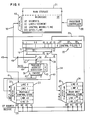
- FIG. 1 is a block diagram showing the relationship of a Processor Controller 20, Main Storage 21, and a Control Store Element (CSE) of a contemporary data processing system. Only that portion of a CSE required to understand the present invention is shown.
- the CSE includes a Control Store Data Register (CSDR) 22 which stores, for each cycle, a microinstruction received on line 23 from either a Read-only control Store (ROS) 24 or a Pageable Control Store (PCS) 25.
- CSDR Control Store Data Register
- ROS Read-only control Store
- PCS Pageable Control Store
- Each microinstruction stored in CSDR 22 includes a number of control fields 26, the decoding of which control the data flow, logic, and arithmetic of a data processing system.
- each microinstruction also includes the information necessary to address the next microinstruction in sequence.
- the address of the next micro- instruction often referred to in the literature as the next address (NA)
- NA next address
- each microinstruction also includes an X-branch control field 27 and a Y-branch control field 28.
- the branch control fields 27 and 28 are coded to select a particular data processing machine condition to provide coded information for accomplishing a microprogram branch.
- branching capability will be discussed subsequently. An understanding of this capability is completely defined in the above cited Reference 2.
- the results of the branching capability are effective on a line 29 in FIG. 1 to select one of four possible microinstructions addressed and accessed from either the ROS 24 or PCS 25 to transfer the selected microinstruction on line 23 to the CSDR 22.
- a microprogrammer who is creating the sequence of microinstructions for the data processing system will have the ability to code each microinstruction in the CSDR 22 to cause address and accessing of microinstructions from either the ROS 24 or PCS 25. This selection is made by the state of NA bit position 0. A binary "0" will cause the remainder of the NA bit positions to be effective at Address Decode 30 to effect access and readout of ROS 24. A binary "1" in NA bit position 0 will cause Address Decode 31 associated with PCS 25 to be effective.
- NA bit position 0 is a binary "0"
- the gate 33 will be effective to transfer NA bits 1 through 13 on lines 34 to the address decode 30 of ROS 24.
- NA bit 0 is a binary "1”
- a gate 36 will be enabled to transfer NA bits 1 through 10 on a line 37 to a Pageable Address Directory 38, the function of which will be subsequently described.
- the signal on line 35 will also enable a gate 39 to transfer NA bits 11 through 13 on line 40 to be part of the address utilized in Address Decode 31 of PCS 25.
- the remainder of the address utilized in the address decode 31 of PCS 25 is transferred on line 41 from an Encode mechanism 42 associated with the Pageable Address Directory 38.
- Pageable Address Directory 38 requires a replacement algorithm which is provided by an LRU mechanism 43.
- LRU mechanism 43 The function of the Pageable Address Directory 38, Encode mechanism 42, and LRU mechanism 43 are thoroughly described in the above cited References 3 and 4.
- an area 44 is reserved in Main Storage 21 for the microcode which is to be transferred to the PCS 25 as required.
- the reserved area 44 is loaded with microcode from the Processor Controller 20.
- the 512 bytes are configured to provide 32 microinstructions. These 32 micro- instructions are identified as a "line" of microcode.
- the remainder of the NA bits are configured to provide identification of segments and lines within segments. That is, NA bits 1 through 5 are capable of identifying 32 segments of microcode and NA bits 6 through 10 are capable of identifying 32 lines within a particular segment of microcode.
- the ROS 204 has been designed to permanently store 8K microinstructions. Therefore, whereas the Address Decode mechanism 30 is shown to be receiving 13 NA bits, only NA bits 3 through 13, along with the XY branch selection, are required to provide access to one of the 8K microinstructions.
- the PCS 25 is configured to include 32 lines of microcode totaling 1K micro- instructions.
- each NA specifying a pageable main store address, indicated on line 35 will initiate an associative search in the Pageable Address Directory 38 to determine which line of PCS 25 contains the microcode line being addressed. If the line requested is stored in PCS 25, an associated one of the registers in the Pageable Address Directory 38, indicates the match and its identity will be encoded by Encode mechanism 42 to provide the five address bits required on line 41 to select the proper line in PCS 25. The remainder of the NA bits 11 through 13 will be transferred on line 40 to the Address Decode mechanism 31 to select a branch-group of four microinstructions from the line. The particular one of the microinstructions in the branch-group to be transferred on line 23 to CSDR 22 is selected by the XY Branch Decode 29.
- a signal on line 48 indicating a Miss will be effective at a gate 49 to transfer the NA bits 1 through 10 on line 50 to the Address Decode mechanism 46 to initiate transfer of the 512 bytes comprising the line of microcode required on line 45 to PCS 25.
- the LRU mechanism 43 in accordance with the teaching of Reference 4, will select the line of PCS 25 least- recently used to receive and store the line of microcode. The line of PCS 25 selected by the LRU mechanism 43 will cause the next address bits 1 through 10 to be stored in the associated register of the Pageable Address Directory 38.
- FIG. 2 is a block diagram that includes certain portions of the apparatus disclosed in FIG. 1. The same numeric designation has been utilized. Additional structure of a CSE in a contemporary data processing system is included in FIG. 2.
- a Present Address Register 51 stores the complete address, including the XY branch bits, utilized to access a microinstruction for transfer to the CSDR 22. When the Next Address portion 52 of each micro- instruction is transferred to the address decoding mechanism 30 or 31 shown in FIG. 1, it is transferred on line 53 to the Present Address Register 51. The Present Address Register 51 therefore retains the address of each micro- instruction transferred to, and stored in, CSDR 22 during the cycle that the control fields 26 are effective.
- Another register shown in FIG. 2 is an Auxiliary Address Register 54 which is utilized in the contemporary data processing system to receive, on a line 55, control store address information from a number of other sources during the sequencing of the CSE.
- FIG. 2 shows a line 56 which receives the OP CODE portion of the machine instruction.
- the gate 58 will be enabled to transfer the OP CODE bits on line 59 to the Present Address Register 51. Therefore, the Present Address Register 51 will store a representation of the OP CODE on line 56 during the cycle that the microinstruction accessed on the first cycle is stored in the CSDR 22.
- the apparatus of the subject invention to achieve the above cited result includes a First Cycle Halt Array 60, a ROS Halt Array 61, and an Address Substitute mechanism 62.
- Each of the arrays 60 and 61 has a single bit storage position for each microinstruction that can conceivably create an error condition. If the OP CODE received on line 56 has eight bit positions, as is standard, the First Cycle Halt Array 60 will have 256 bit storage positions.
- the ROS 24 will store 8K microinstructions, and therefore the ROS Halt Array 61 will be comprised of 8K bit storage positions.
- the Processor Controller 20 of FIG. 1 is utilized during the initialization of the data processing system to provide the proper pattern of binary "1" and binary "0" for the First Cycle Halt Array 60 or the ROS Halt Array 61. This information is created by maintenance personnel, and during the initialization process, will be input to the arrays on lines 66, 67 and 68. As the need for changes to microinstruction execution are noted, the proper bit patterns will be created by maintenance personnel for storage in the halt arrays at the address associated with the microinstruction to be inhibited.
- the address stored in the Present Address Register 51 of the microinstruction for which a substitute microinstruction is to be accessed is transferred on a line 69 through a gate 70 to the Address Substitute mechanism 62.
- the Address Substitute mechanism 62 will then effect a translation of the address stored in the Present Address Register 51 to a main storage address for transfer on line 71 to the Auxiliary Address Register 54.
- bit position 0 of the Present Address Register 51 shown as a binary "0" at 72, will be translated to a binary "1" shown at 73 in the Auxiliary Address Register 54.
- the address stored in Auxiliary Address Register 54 which is a main storage address, will be transferred on line 74 to the Pageable Address Directory 38 to initiate a normal PCS 25 access function as described in connection with FIG. 1.
- the Processor Controller 20 of FIG. 1 is utilized to input information on lines 66 and 75 to provide, during the initialization process, the address in Main Storage 21 of FIG. 1 of the microinstruction to be substituted for the erroneous microinstruction.
- the main storage address on line 75 to be associated with the erroneous microinstruction address in Present Address Register 51, will be stored in the Address Substitute mechanism 62 to thereafter be generated on line 71 whenever the erroneous microinstruction address is utilized.
- FIG. 3 shows a number of alternative methods by which main storage addresses for the substitute microinstruction can be created for entry into the Address Substitute mechanism 62 of FIG. 2.
- One technique would require each of the 8K ROS addresses 76 to be provided with an associated main storage address 77 creating an 8K storage patch area 77.
- the only requirement for the Address Substitute mechanism 62 of FIG. 2 is to convert the address position 72 in the Present Address Register 51 from a binary "0" to a binary "1" in the Auxiliary Address register 54.
- This alternative creates a very simple Address Substitute mechanism 62, but is very wasteful of main storage address space in that 8K main storage microinstruction addresses must be permanently reserved.
- FIG. 3 Another alternative is shown in FIG. 3 where the next address (NA) bits 53 are utilized to address an 8K Address Substitute Table 78. That is, each possible 8K ROS address will have an addressable entry in the Address Substitute Table 78 only if the particular address provides access to an erroneous microinstruction. Therefore, the Address Substitute mechanism 62 of FIG. 2 would not only detect an erroneous microinstruction, but provides the ability to reserve only one main storage position for each bad ROS position as indicated at 79. Therefore, with the inclusion of a comparatively expensive Address Substitute Table 78, a great deal of compression can be realized in Main Storage 21 with very little space set aside for substitute microinstructions.
- NA next address
- FIG. 3 A preferred result for the Address Substitute mechanism 62 of FIG. 2 will be described subsequently, and is represented in FIG. 3 at 80 and 81.
- An 8K ROS address space 80 can be compressed to a Storage Patch Area 81 which is a compromise between the amount of main storage addresses that must be reserved for substitute microinstructions, and the expense and efficiency of the address translation performed by the Address Substitute mechanism 62 of FIG. 2.
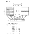
- the 8K ROS addresses 80 range from 0000 to 1FFF (each position representing a hexadecimal digit comprised of four binary bits), to a Storage Patch Area 81 which ranges from main storage addresses F800 through FFFF, a total of 2K microinstruction addresses. Hexadecimal notation is fairly common, but the particular representation of four binary bits representing a hexadecimal digit is shown in FIG. 5.
- a fairly common random access storage provides a storage module containing 256 addressable locations, which in most cases provide storage for 8 binary bits in each location.
- the First Translation Array 86 and Second Translation Array 87 each utilize 8 binary bits for addressing.
- First and second fields of the address information in the Present Address Register 51 are utilized.
- the first and second fields are caused to overlap in three bit positions.
- the First Translation Array 86 is addressed by a first portion comprised of the Present Address Register 51, bit positions 3 through 10, and the Second Translation Array 87 is addressed by a second portion comprised of bit positions 8 through 15.
- the First Translation Array 86 will provide 7 substitute address bits and the Second Translation Array 87 will provide 6 substitute address bits. Individual bit positions from the outputs of the First Translation Array 86 and Second Translation Array 87 are transferred to the Auxiliary Address Register 54 in an interleaved manner. When the substitute address has been generated and transferred to the Auxiliary Address Register 54, bit positions 1 through 10 are transferred to the Pageable Address Directory 38 on line 74.
- FIGS. 5 and 6 show the main storage address compression capabilities of the embodiments of the Address Substitute mechanism 62 shown in more detail in FIG. 4.
- eight consecutive ROS addresses are assumed to be in error requiring translations to a final pageable address for utilization in the PCS 25 accessing mechanism of FIG. 1.
- FIG. 5 shows a configuration possible as a modification to FIG. 4 wherein the first and second portions of the ROS address presented to the First Translation Array 86 and Second Translation Array 87 are not overlapped.
- the final pageable address compression capability that can be realized by interleaving the outputs of the translation arrays into Auxiliary Address Register 54 is shown.
- the interleaving of the output bits of the First Translation Array 86 and Second Translation Array 87 requires a main storage address ranging only from "0" through "42" to accommodate the eight consecutive ROS addresses in error.
Landscapes
- Engineering & Computer Science (AREA)
- Software Systems (AREA)
- Theoretical Computer Science (AREA)
- Physics & Mathematics (AREA)
- General Engineering & Computer Science (AREA)
- General Physics & Mathematics (AREA)
- Memory System Of A Hierarchy Structure (AREA)
Claims (2)
Applications Claiming Priority (4)
| Application Number | Priority Date | Filing Date | Title |
|---|---|---|---|
| US26914781A | 1981-06-01 | 1981-06-01 | |
| US26914681A | 1981-06-01 | 1981-06-01 | |
| US269147 | 1981-06-01 | ||
| US269146 | 1981-06-01 |
Publications (2)
| Publication Number | Publication Date |
|---|---|
| EP0066083A1 EP0066083A1 (de) | 1982-12-08 |
| EP0066083B1 true EP0066083B1 (de) | 1986-07-16 |
Family
ID=26953537
Family Applications (1)
| Application Number | Title | Priority Date | Filing Date |
|---|---|---|---|
| EP82103547A Expired EP0066083B1 (de) | 1981-06-01 | 1982-04-27 | Einrichtung zur Adressensubstitution |
Country Status (2)
| Country | Link |
|---|---|
| EP (1) | EP0066083B1 (de) |
| DE (1) | DE3272001D1 (de) |
Citations (1)
| Publication number | Priority date | Publication date | Assignee | Title |
|---|---|---|---|---|
| US3764996A (en) * | 1971-12-23 | 1973-10-09 | Ibm | Storage control and address translation |
Family Cites Families (2)
| Publication number | Priority date | Publication date | Assignee | Title |
|---|---|---|---|---|
| GB1483442A (en) * | 1975-10-09 | 1977-08-17 | Standard Telephones Cables Ltd | Computing machine including a directly addressable memory arrangement |
| NL7807314A (nl) * | 1978-07-06 | 1980-01-08 | Philips Nv | Inrichting voor het vergroten van de lengte van een logisch computeradres. |
-
1982
- 1982-04-27 DE DE8282103547T patent/DE3272001D1/de not_active Expired
- 1982-04-27 EP EP82103547A patent/EP0066083B1/de not_active Expired
Patent Citations (1)
| Publication number | Priority date | Publication date | Assignee | Title |
|---|---|---|---|---|
| US3764996A (en) * | 1971-12-23 | 1973-10-09 | Ibm | Storage control and address translation |
Non-Patent Citations (2)
| Title |
|---|
| IBM Technical Disclosure Bulletin, vol. 23, no. 10, March 1981, pp. 4627-4628 * |
| IEEE Transactions on Industrial Electronics and Control Instrumentation, vol. IEC I-23, no. 3, Aug. 1976, pp. 200-206 * |
Also Published As
| Publication number | Publication date |
|---|---|
| EP0066083A1 (de) | 1982-12-08 |
| DE3272001D1 (en) | 1986-08-21 |
Similar Documents
| Publication | Publication Date | Title |
|---|---|---|
| EP0066084B1 (de) | Anordnung zur Mikrobefehlsubstitution in einem Programmspeicher | |
| US4591972A (en) | Data processing system with unique microcode control | |
| EP0204832B1 (de) | Fehler entdeckendes und fehler korrigierendes system | |
| US3979726A (en) | Apparatus for selectively clearing a cache store in a processor having segmentation and paging | |
| US4361868A (en) | Device for increasing the length of a logic computer address | |
| EP0415461B1 (de) | Zentrale Verarbeitungseinheit mit der Fähigkeit, Befehle mit variablen Längen zu unterstützen | |
| US4386399A (en) | Data processing system | |
| US4853849A (en) | Multi-tasking register set mapping system which changes a register set pointer block bit during access instruction | |
| CA1109967A (en) | Expandable microprogram memory | |
| US4569018A (en) | Digital data processing system having dual-purpose scratchpad and address translation memory | |
| US3753236A (en) | Microprogrammable peripheral controller | |
| US3800291A (en) | Data processing system memory relocation apparatus and method | |
| US3990054A (en) | Microprogram organization techniques | |
| US4398243A (en) | Data processing system having a unique instruction processor system | |
| US4124893A (en) | Microword address branching bit arrangement | |
| US4597041A (en) | Method and apparatus for enhancing the operation of a data processing system | |
| US4747044A (en) | Direct execution of software on microprogrammable hardware | |
| US4493033A (en) | Dual port cache with interleaved read accesses during alternate half-cycles and simultaneous writing | |
| EP0039227A2 (de) | Datenverarbeitungsanlage | |
| US5414821A (en) | Method of and apparatus for rapidly loading addressing environment by checking and loading multiple registers using a specialized instruction | |
| US4893235A (en) | Central processing unit for a digital computer | |
| EP0066083B1 (de) | Einrichtung zur Adressensubstitution | |
| US4510582A (en) | Binary number substitution mechanism | |
| US4531199A (en) | Binary number substitution mechanism in a control store element | |
| EP0066082B1 (de) | Mikrobefehls-Steuerspeichersystem |
Legal Events
| Date | Code | Title | Description |
|---|---|---|---|
| PUAI | Public reference made under article 153(3) epc to a published international application that has entered the european phase |
Free format text: ORIGINAL CODE: 0009012 |
|
| AK | Designated contracting states |
Designated state(s): DE FR GB |
|
| 17P | Request for examination filed |
Effective date: 19830420 |
|
| GRAA | (expected) grant |
Free format text: ORIGINAL CODE: 0009210 |
|
| AK | Designated contracting states |
Kind code of ref document: B1 Designated state(s): DE FR GB |
|
| REF | Corresponds to: |
Ref document number: 3272001 Country of ref document: DE Date of ref document: 19860821 |
|
| ET | Fr: translation filed | ||
| PLBE | No opposition filed within time limit |
Free format text: ORIGINAL CODE: 0009261 |
|
| STAA | Information on the status of an ep patent application or granted ep patent |
Free format text: STATUS: NO OPPOSITION FILED WITHIN TIME LIMIT |
|
| 26N | No opposition filed | ||
| PGFP | Annual fee paid to national office [announced via postgrant information from national office to epo] |
Ref country code: FR Payment date: 19900328 Year of fee payment: 9 |
|
| PGFP | Annual fee paid to national office [announced via postgrant information from national office to epo] |
Ref country code: GB Payment date: 19900331 Year of fee payment: 9 |
|
| PGFP | Annual fee paid to national office [announced via postgrant information from national office to epo] |
Ref country code: DE Payment date: 19900427 Year of fee payment: 9 |
|
| PG25 | Lapsed in a contracting state [announced via postgrant information from national office to epo] |
Ref country code: GB Effective date: 19910427 |
|
| PG25 | Lapsed in a contracting state [announced via postgrant information from national office to epo] |
Ref country code: FR Effective date: 19911230 |
|
| GBPC | Gb: european patent ceased through non-payment of renewal fee | ||
| PG25 | Lapsed in a contracting state [announced via postgrant information from national office to epo] |
Ref country code: DE Effective date: 19920201 |
|
| REG | Reference to a national code |
Ref country code: FR Ref legal event code: ST |