EP0066263B1 - Halbleiteranordnung mit zwei Widerständen - Google Patents
Halbleiteranordnung mit zwei Widerständen Download PDFInfo
- Publication number
- EP0066263B1 EP0066263B1 EP82104644A EP82104644A EP0066263B1 EP 0066263 B1 EP0066263 B1 EP 0066263B1 EP 82104644 A EP82104644 A EP 82104644A EP 82104644 A EP82104644 A EP 82104644A EP 0066263 B1 EP0066263 B1 EP 0066263B1
- Authority
- EP
- European Patent Office
- Prior art keywords
- resistor
- resistors
- ion
- type
- region
- Prior art date
- Legal status (The legal status is an assumption and is not a legal conclusion. Google has not performed a legal analysis and makes no representation as to the accuracy of the status listed.)
- Expired
Links
- 239000004065 semiconductor Substances 0.000 title claims description 42
- 239000012535 impurity Substances 0.000 description 25
- 238000009792 diffusion process Methods 0.000 description 11
- 239000004020 conductor Substances 0.000 description 10
- 238000005468 ion implantation Methods 0.000 description 10
- 230000015572 biosynthetic process Effects 0.000 description 9
- 238000010420 art technique Methods 0.000 description 7
- 239000000758 substrate Substances 0.000 description 5
- 238000010438 heat treatment Methods 0.000 description 4
- 230000002349 favourable effect Effects 0.000 description 2
- 238000002955 isolation Methods 0.000 description 2
- 238000011282 treatment Methods 0.000 description 2
- ZOXJGFHDIHLPTG-UHFFFAOYSA-N Boron Chemical compound [B] ZOXJGFHDIHLPTG-UHFFFAOYSA-N 0.000 description 1
- OAICVXFJPJFONN-UHFFFAOYSA-N Phosphorus Chemical compound [P] OAICVXFJPJFONN-UHFFFAOYSA-N 0.000 description 1
- 230000001133 acceleration Effects 0.000 description 1
- 230000003213 activating effect Effects 0.000 description 1
- 238000000137 annealing Methods 0.000 description 1
- 229910052796 boron Inorganic materials 0.000 description 1
- 230000007423 decrease Effects 0.000 description 1
- 238000011161 development Methods 0.000 description 1
- 230000018109 developmental process Effects 0.000 description 1
- 238000005530 etching Methods 0.000 description 1
- 150000002500 ions Chemical class 0.000 description 1
- 238000004519 manufacturing process Methods 0.000 description 1
- 239000002184 metal Substances 0.000 description 1
- 229910052698 phosphorus Inorganic materials 0.000 description 1
- 239000011574 phosphorus Substances 0.000 description 1
- 238000007789 sealing Methods 0.000 description 1
Images






Classifications
-
- H—ELECTRICITY
- H10—SEMICONDUCTOR DEVICES; ELECTRIC SOLID-STATE DEVICES NOT OTHERWISE PROVIDED FOR
- H10D—INORGANIC ELECTRIC SEMICONDUCTOR DEVICES
- H10D84/00—Integrated devices formed in or on semiconductor substrates that comprise only semiconducting layers, e.g. on Si wafers or on GaAs-on-Si wafers
- H10D84/201—Integrated devices formed in or on semiconductor substrates that comprise only semiconducting layers, e.g. on Si wafers or on GaAs-on-Si wafers characterised by the integration of only components covered by H10D1/00 or H10D8/00, e.g. RLC circuits
- H10D84/204—Integrated devices formed in or on semiconductor substrates that comprise only semiconducting layers, e.g. on Si wafers or on GaAs-on-Si wafers characterised by the integration of only components covered by H10D1/00 or H10D8/00, e.g. RLC circuits of combinations of diodes or capacitors or resistors
- H10D84/209—Integrated devices formed in or on semiconductor substrates that comprise only semiconducting layers, e.g. on Si wafers or on GaAs-on-Si wafers characterised by the integration of only components covered by H10D1/00 or H10D8/00, e.g. RLC circuits of combinations of diodes or capacitors or resistors of only resistors
Definitions
- the present invention relates to a semiconductor device, and more particularly to a resistor having a high resistance value in a monolithic integrated circuit (hereinafter called "monolithic IC").
- a resistor in a monolithic IC for instance, in a bipolarmonolithic IC comprising circuit elements formed in an N-type epitaxial layer on a P-type substrate, is normally constructed of a P-type strip-shaped region formed in the N-type epitaxial layer simultaneously with formation of a base region of an NPN transistor.
- the sheet resistance and junction depth of the strip-shaped region are uniquely determined depending upon a characteristic of the NPN transistor. Therefore, a predetermined resistance value is realized by adjusting width and/or length of the strip-shaped region.
- the sheet resistance of the strip-shaped region is low. For this reason, in order to obtain a resistor having a high resistance value, the length of the strip-shaped region would become very long. As a result, the area occupied by the strip-shaped region would become very large.
- the so-called pinch resistor and ion-implanted resistor have been used. These resistors have been employed also in MOS-type monolithic IC.
- the pinch resistor is such that an N'-type region is formed on the P-type strip-shaped resistor region so as to overlap with a part of the P-type strip-shaped resistor region and to connect with the N-type region in which the P-type resistor region has been formed and electrical. connection is provided at the both ends of the strip-shaped resistor region.
- the thickness of the strip-shaped region is partially reduced by the overlapping N+ -type region, and moreover, the portion having a relatively high impurity concentration along the surface of the strip-shaped region would not contribute to the determination of the resistance value.
- the resistance value is substantially determined by the sheet resistance of a P-type portion under the overlapping N'-type region and the width and length of this overlapped P-type portion.
- the sheet resistance of the P-type portion is increased by about one decimal order.
- the ion-implanted resistor is constituted by an ion-implanted region having a high sheet resistance, i.e., by a strip-shaped region formed by implanting P-type impurity ions into a surface portion of an N-type region at a low concentration. Since the sheet resistance of the ion-implanted region is relatively high, good ohmic contact between an electrode and the ion-implanted region cannot be realized. Hence, contact regions having a low sheet resistance are formed at both ends of the strip-shaped region, and electrodes for the ion-implanted resistor are formed on the contact regions.
- the resistance value of the ion-implanted resistor is substantially determined by such a portion of the ion-implanted region that is located between the contact regions.
- the formation of the ion-implanted region by the ion-implantation of an impurity is effected before the formation of the electrodes but after active regions for circuit elements have been formed. If heat treatments for forming the active regions are effected after ion-implantation of impurities, the implanted impurities would be rediffused by the heat treatments, so that a desired high sheet resistance could not be obtained.
- a thickness of a surface insulating film on the ion-implanted region is extremely thin as compared to that of the surface insulating film on its surrounding region which has been formed through several times of heat treatment included in the diffusion steps effected before the ion implantation step.
- the difference in thickness between the surface insulating film on the ion-implanted region and that on its surrounding region is considerably large. For this reason, in the event that an interconnection conductor passes over an ion-implanted resistor, it may possibly occur that the interconnection conductor is broken at the steps of the insulating films.
- a semiconductor region is additionally formed simultaneously with the contact regions in the ion-implanted resistor.
- the interconnection conductor crosses above this semiconductor region, the insulating film on which is found thick by the subsequent steps including the heat treatment. Since this semiconductor region has a low sheet resistance, the ion-implanted region is elongated by the length corresponding to the length of that semiconductor region. Consequently, an ion-implanted resistor over which an interconnection conductor passes includes at least two ion-implanted resistor regions, two contact regions and a semiconductor region having a low sheet resistance for connecting the two ion-implanted resistor regions to each other. This semiconductor region is referred to, hereinafter, as a connecting region.
- pinch resistors and ion-implanted resistors are used as resistors in a circuit such as, for example, a differential amplifier, a flip-flop or resistance divider circuit which requires a precise resistance ratio, a current flowing through the circuit could be reduced for a low power consumption, and further the design of a heat capacity of a package for sealing a semiconductor chip could become easy.
- a circuit such as, for example, a differential amplifier, a flip-flop or resistance divider circuit which requires a precise resistance ratio
- contact regions and the connecting region occurring in their formation directly influence the resistance value of the ion-implanted resistor. More particularly, with the expansion of the N'-type region in the pinch resistor, the length of the P-type portion overlapped with the N'-type region is undesirably expanded, so that the resistance value of the pinch resistor becomes higher. On the other hand, the expansion of contact regions and the connecting region in the ion-implanted resistor undesirably decreases the length of the ion-implanted resistor region between them, so that the resistance value of the ion-implanted resistor becomes lower.
- a semiconductor device including two resistors, one resistor being formed of one unit resistor region and the other resistor being formed of a plurality of unit resistor regions connected in series by metal conductors. Each unit resistor region is isolated individually by a P-N junction.
- resistors of this type which are made up by series-connected individual, substantially identical unit resistor regions the above described problem which occurs in resistors formed by differently treated zones of a continuous elongated semiconductor region does not occur.
- Another object of the present invention is to provide a semiconductor device in which a resistance ratio between resistors having different configurations can be precisely achieved.
- a semiconductor device comprises first and second resistor regions of one conductivity type formed in a semiconductor region of opposite conductivity type.
- the first and second resistor regions have different configurations from each other.
- the first resistor region includes a plurality of first portions which contribute to the determination of the resistance value of the first resistor
- the second resistor region includes at least one second portion which contributes to the determination of the resistance value of the second resistor.
- the ratio of the number (two or more) of the first portions to number (one or more) of the second portion is made identical to the intended ratio in the resistance value of the first resistor to the second resistor. It is favorable that the first and second resistor regions have the same width.
- the width of the respective first portions is the same and substantially equal to the width of the at least one second portion and the ratio of the sum of the lengths of all the first portions to the total length of the at least one second portion is made equal to the intended resistance ratio of the first and second resistors.
- a semiconductor device in the case where the first and second resistors are pinch resistors, a semiconductor device according to the present invention further comprises a plurality of third semiconductor regions of the opposite conductivity type overlapping the respective first portions and at least one fourth semiconductor region overlapping the second portion. Consequently, the first and second portions in the first and second resistor regions are pinched between the common semiconductor region and the third and fourth semiconductor regions, respectively.
- the first and second resistors are ion-implanted resistors
- the first and second portions are the portions in the first and second resistor regions having an inherent sheet resistance obtained by ion implantation, respectively, located between two of contact regions and connecting resistions.
- two third semiconductor regions are provided in the case of pinch resistors, while in the case of ion-implanted resistors, there are two portions in the first resistor region having the inherent sheet resistance obtained by ion implantation and located between contact regions and a connecting region.
- the two first portions in the pinch resistors are connected by the portion in the first resistor region on which the third semiconductor region is not formed, while the two first portions in the ion-implanted resistors are connected by the portion (i.e. a connecting region) in the first resistor region having a sheet resistance lower than that obtained by the ion implantation.
- the portion for connecting the two first portions to each other is not substantially contribute to the determination of the resistance value of the first resistor, because it has a considerably small sheet resistance as compared to that of the first portions.
- the ratio of the number of the first portions to that of the second portion or portions is determined so as to coincide with the intended ratio of the resistance value of the first resistor to that of the second resistor. For instance, if the resistance ratio is 2, then the ratio in the number of the first portions to the second portion is also chosen to be 2. Accordingly, in the case of pinch resistors, the ratio of the error caused by the expansion of the third semiconductor regions in the first resistor to that caused by the expansion of the fourth semiconductor region in the second resistor becomes identical to the resistance ratio of the first resistor to the second resistor. In other words, the resistance ratio between the pinch resistors can be precisely obtained.
- the ratio of the error caused by the expansions of the contact regions and the connecting region in the first resistor to that caused by the expansion of the contact regions and the connecting region in the second resistor becomes identical to the resistance ratio of the first resistor to the second resistor, so that the resistance ratio between the ion-implanted resistors can be precisely achieved. Therefore, the pinch resistors or ion-implanted resistors according to the present invention can be used as the resistors in the circuit which requires a precise resistance ratio. As a result, the reduction of a circuit current can be achieved, and a freedom in design of a heat capacity of a package also can be enhanced.
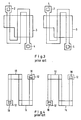
- Figure 1 shows two pinch resistors R, and R 2 which have been produced in accordance with the prior art technique aiming at a resistance ratio of 1:1.
- the pinch resistors R, and R 2 are produced by forming, for instance, P-type diffused layers 2 and 5 in an N-type semiconductor layer 1 and further forming N--type diffused layers 3 and 6 so as to partly overlap with the diffused layers 2 and 5, respectively.
- the both end portions of the diffused layers 2 and 5 are broadened, and contact windows 4 and 7 for electrodes are formed on the broadened portions.
- the P-type diffused layer 2 in the resistor R is formed in an S-shape, and the P-type diffused layer 5 in the resistor R 2 is formed in a W-shape.
- the N + -type diffused layer 3 overlaps with three portions of the P-type diffused layer 2, and the N + -type diffused layer 6 overlaps four portions of the P-type diffused layer 5. Since P-type portions 8 and 9 pinched between the N'-type diffused layers 3 and 6 and the N-type semiconductor layer 1 have a high sheet resistance, these portions determine essentially the resistance values of resistors R, and R 2 .
- the portions of the P-type diffused layers 2 and 5 other than the P-type portions 8 and 9 does not substantially contribute to the resistance values of the resistors R, and R 2 due to their low sheet resistances.
- the resistance value of the resistor R is substantially determined by the three P-type portions 8, and that of the resistor R 2 is substantially determined by the four P-type portions 9.
- solid line contours 2, 5, 3 and 6 of the diffused layers are designed configurations in a mask pattern, while chain line contours 2', 5', 3' and 6' of the diffused layers indicate the configurations after impurities have been diffused.
- the configurations of the diffused layers are, in practice, enlarged as compared to the designed configurations because of the lateral diffusion of the impurities.
- the impurity concentration of the N + -type diffused layers 3 and 6 is high, and therefore the lateral enlargement of the N'-type diffused layers 3 and 6 is larger than that of layers 2 and 5.
- the resistance ratio between the pinch resistors R 1 and R 2 having the aforementioned configurations will be considered.
- a simplified formula for generally representing a resistance value R of a pinch resistor is given by the following equation: where ⁇ PINCH represents a sheet resistance of a P-type portion pinched between two N-type layers; W and L represent a width and a length on a mask pattern of the P-type portion, respectively; and AW and AL represent increments of the width W and the length L caused by the lateral diffusion of the impurities, respectively.
- the ⁇ W and ⁇ L have a positive sign due to the expansion of the upper N + -type layer as well as the expansion of the P-type layer.
- a a sum of the contact resistances of electrodes (not shown) connected to the layer 2 through the contact windows 4 and the resistances of the portions of the P-type diffused layer 2 on which the N + -type diffused layer 3 is not formed.
- Equation-(2) The second term on the right side of Equation-(2) is negligibly small as compared to the first term on the right side. Hence, Equation-(2) can be reduced into the following equation:
- Equation-(6) represents that as the ratio between the numbers n and n' differs from an intended resistance ratio, that is, from the total length ratio ⁇ of the P-type portions, the resistance ratio between the resistors R 1 and R 2 would deviate from the intended resistance ratio. Therefore, in order to eliminate the deviation of the resistance ratio between the resistors R 1 and R 2 , it is required to select the numbers n and n' of the overlapped portions in Equation-(6) in accordance with the resistance ratio. In the case where the resistance ratio is one, the number n should be selected to equal the number n'.
- the P-type diffused layer 2 was formed in the same W-shape as the P-type diffused layer 5 or the P-type diffused layer 5 was formed in the same S-shape as the P-type diffused layer 2.
- the resistor R 1 and the resistor R 2 were formed in the congruent configuration. This would bring about the restriction in a pattern layout.
- the resistance ratio is larger than 1 or the configurations between two resistors are different as shown in Figure 2, a precise resistance ratio could not be realized due to the different configurations of the two resistors.
- the ion-implanted resistors have P-type ion-implanted regions 11 and 15 having a high sheet resistance which are formed in an N-type layer 10 through the ion-implantation of P-type impurities, and further have P-type contact regions 12 and 16 having a high impurity concentration which are formed at both ends of the P-type ion-implanted regions 11 and 15 simultaneously with formation of a base region, respectively.
- the resistors R 3 and R 4 are formed in an S-shape and in a U-shape, respectively.
- the resistor configurations shown in Figure 2 can meet the case where interconnection conductors have to pass over the ion-implanted resistors R 3 and R 4 in the point of view of a wiring pattern, respectively.
- the ion-implanted resistors R 3 and R 4 are provided with regions 13 and 17 having a low sheet resistance, respectively. The interconnection conductor passing over the resistor R 3 crosses over the region 13, while the interconnection conductor passing over the resistor R 4 crosses over the region 17.
- this region 14 may be formed as an ion-implanted region connected to the ion-implanted regions 11. However, if it should be done, two bent corners would arise in the ion-implanted region 11 of the resistor R 3 . On the other hand, in the resistor R 4 there is no bent corner of the ion-implanted region 15. Thus, if there exists a difference in the number of bent corners of ion-implanted regions between two resistors, the desired resistance ratio between the resistors R 3 and R 4 cannot be obtained due to fluctuations in the resistance at the bent corner.
- the resistance value of the resistor R 3 is substantially determined by three ion-implanted regions 11, while that of the resistor R 4 is substantially determined by two ion-implanted regions 15.
- the regions 12, 13, 14, 16 and 17 are formed simultaneously.
- the regions 12, 13, 14, 16 and 17 are formed earlier than the ion-implanted regions 11 and 15.
- Contact windows 18 and 19 are provided in surface insulating films (not shown) on the contact regions 12 and 16, respectively.
- solid line contours of the regions 12, 13, 14, 16 and 17 indicate designed configurations on a mask pattern, whereas chain line contours 12', 13', 14', 16' and 17' indicate resistor configurations that can be really obtained after the diffusion of impurities.
- solid line contours of the regions 11 and 15 indicate the configurations on a mask pattern to be used for ion-implantation
- chain line contours 11' and 15' indicate the configurations of the ion-implanted regions really produced by the anneal treatment for activating the ion-implanted impurities. Since the impurity concentration of regions 12, 13, 14, 16 and 17 is high, these regions expand more than the ion-implanted regions 11 and 15.
- a simplified formula for generally representing a resistance R of an ion-implanted resistor is given by the following equation: where p s represents a sheet resistance of an ion-implanted region; L and W represent a length and a width of the ion-implanted region on a mask pattern; AW represents an increment of the width of the ion-implanted region caused by anneal treatment; and AL represents a decrement of the length of the ion-implanted region caused by expansion of the contact regions 12 and 16 and the regions 13, 14 and 17, and therefore, the actual length of the ion-implanted region is reduced.
- a represents the sum of the contact resistances of electrodes (not shown) connected to contact regions 12 and 16 through the windows 18 and 19 and the resistances of the regions 13, 14, and 17.
- the resistance ratio R 4 /R 3 between the resistors R 4 and R 3 can be represented by the following equation:
- Equation-(10) where n and n' represent the numbers of the ion-implanted regions 11 and 15, respectively, and ⁇ represents the ratio of the total length of all the ion-implanted regions 15 in the resistor R 4 to that of all the ion-implanted regions 11 in the resistor R 3 .
- Equation-(11) represents that as the ratio between the numbers n and n' differs from an intended resistance ratio, that is, from the total length ratio ⁇ of the ion-implanted regions, the resistance ratio between the resistors R 3 and R 4 would deviate from the intended resistance ratio. Therefore, in order to eliminate the deviation of the resistance ratio between the resistors R 3 and R 4 in the case where the intended resistance ratio is one, it is necessary to select the numbers n and n' in Equation-(11) to be equal to each other.
- the numbers of the ion-implanted regions 11 and 15 were equalized either by adding one ion-implanted region in one resistor or reducing one ion-implanted region in the other resistor, and also the numbers of bent corners of the ion-implanted regions in the respective resistors were equalized.
- this measure taken in the prior art implies that the resistors R 3 and R 4 are formed in a congruent shape, resulting in bringing about severe restriction to a pattern layout.
- the shapes of two resistors are different as shown in Figure 2 or a resistance ratio larger than 1 is required, it is absolutely impossible to realize a precise resistance ratio.
- Figure 5 shows the application of the present invention to the two resistors R 1 and R 2 shown in Figure 1.
- reference symbols similar to those appearing in Figure 1 designate like physical quantities and reference numerals similar to those appearing in Figure 1 designate like component parts.
- the number n of the P-type portions 8 pinched between the N-type epitaxial layer 1 and the N + -type diffused layer 3 in the resistor R,' is increased to 4 by modifying the shape of the N'-type diffused layer 3 in the resistor R 1 ' without varying the shapes of the P-type diffused layers 2 and 5 in the resistors R 1 ' and R 2 '.
- four P-type portions 8 determines the resistance value of the resistor R 1 ' like the resistor R 2 '.
- the lengths L 2 ' and L 3 ' of two P-type portions 8 are chosen to be equal to the lengths L 2 and L 3 of the P-type portions 8 in Figure 1, then the sum L 1 '+L 8 of the lengths of other two P-type portions 8 is selected equal to the length L, in Figure 1.
- the numbers n and n' of the overlapped portions between the N--type diffused layers 3 and 6 and the P-type diffused layers 2 and 5 in the resistors R 1 ' and R 2 ' are both equal to 4.
- Figure 6 shows application of the present invention to the two ion-implanted resistors R 3 and R 4 shown in Figure 2.
- reference numerals similar to those appearing in Figure 2 designate like component parts.
- the number n' of the ion-implanted regions which contribute to determination of the resistance value of the resistor R 4 ' is increased to 3 by additionally forming a P-type region 17' in one part of the left side ion-implanted region 15' in the resistor R 4 '.
- the resistance ratio R 4 '/R 3 ' between the resistors R 3 ' and R 4 ' can be derived as follows: In other words, even if the configurations of the ion-implanted regions are different, there are provided two resistors R 3 ' and R 4 ' having a precisely defined resistance ratio therebetween.
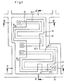
- Figure 7 is a plan view showing two pinch resistors R io and R 11 fabricated according to one preferred embodiment of the present invention. Cross-section views taken along lines A-A', B-B' and C-C' in Figure 7 are shown in Figures 8, 9 and 10, respectively. These two resistors R, o and R 11 are formed in a bipolar monolithic IC. More particularly, formed on a P-type substrate 30 is an N-type epitaxial layer 31 of 8.6 pm to 9.7 pm in thickness having a resistivity of 0.88 ohm-cm to 1.18 ohm-cm. The N-type epitaxial layer 31 is divided into a plurality of island regions by an isolation region 32.
- a P-type impurity such as boron or the like is selectively diffused into one island region 31' simultaneously with the formation of base regions (not shown) of NPN transistors, and thereby P-type regions 33 and 33' are formed in the shapes shown in Figure 7.
- the P-type region 33 bends substantially at a right angle 6 times between the electrodes at the both ends, while the P-type region 33' bends substantially at a right angle 4 times between the electrodes at the both ends.
- the regions 33 and 33' both have a depth of about 2.8 ⁇ m and a sheet resistance of 150 to 250 ohm/.
- N + -type regions 34 and 34' are formed in the shapes shown in Figure 7 by selectively diffusing an N-type impurity such as phosphorus or the like simultaneously with the formation of emitter regions (not shown) of the NPN transistors.
- the depth of the regions 34 and 34' is 2.0 ⁇ m and their sheet resistance is 2 to 10 ohm/--. Under such a condition, the P-type portions under the regions 34 and 34' have a depth of 0.8 pm and a sheet resistance of 4 kohm/-.
- the resistance value of the resistor R 10 is determined by the resistances of two P-type portions 33-1 and 33-2 ( Figure 9) pinched between the N + -type region 34 and the N-type epitaxial layer 31.
- the length of the P-type portions 33-1 and 33-2 are represented by L 10 and L 11 , respectively. It is to be noted that the P-type portion 33-1 includes 4 bent corners, and the P-type portion 33-2 has no bent corner.
- the resistor R " which is required to have a precisely defined resistance ratio of 1:1 with respect to the resistor R 10 having the above-described configuration, has its resistance value determined by the shape of the N + -type region 34' as will be described in the following.
- the P-type portion 33-1 which determines the resistance value of the resistor R 10 in cooperation with the P-type portion 33-2 has four bent corners, and the P-type portion 33-2 has no bent corner. Therefore, it is preferable that also in the resistor R " , P-type portions determining its resistance value have four bent corners.
- the shape of the N + -type region 34' is determined such that in the resistor R11, a P-type portion 33'-1 pinched between the N +- type region 34' and the N + -type epitaxial layer 31 which determine the resistance value of the resistor R 11 also have four bent corners.
- a desired resistance value of the resistor R, o is realized by two P-type portions 33-1 and 33-2.
- the N-type region 34' is shaped so as to include a portion overlapping with the P-type region 33' and a portion not overlapping with the P-type region 33'.
- two P-type portions 33'-1 and 33'-2 determine the resistance value of the resistor R 11 .
- the resistance ratio R 11 /R 10 between the resistors R io and R 11 is derived as follows: In other words, a precise resistance ratio of 1:1 can be realized regardless of the lateral diffusion of impurities in the N +- type regions 34 and 34'.
- FIG. 11 A second preferred embodiment of the present invention is illustrated in Figure 11.
- the resistance value of a pinch resistor R 20 is designed to be twice as large as that of a pinch resistor R 21 .
- the pinch resistors R 20 and R 21 are formed in an epitaxial layer 40.
- the pinch resistor R 20 comprises a rectilinear P-type diffused layer 41 and a comb-shaped N + -type diffused layer 42 having 6 teeth intermittently overlapping with the surface of the P-type diffused layer 41.
- Contact windows 45 for electrodes are formed at the both ends of the P-type diffused layer 41.
- the pinch resistor R 21 comprises a P-type diffused layer 41' having 4 bent corners and a rectilinear N +- type diffused layer 42' overlapping with the surface of the P-type diffused layer 41' at 3 locations.
- contact windows 46 for electrodes are formed at the both ends of the P-type diffused layer 41'.
- the total length of the six P-type portions overlapped with the N + -type region 42 is chosen to be twice as large as that of the three P-type portions overlapped with the N-type region 42'.
- the illustrated embodiment provides a design of two pinch resistors R 2o and R 21 in the cases where the P-type region 41 should have an elongated shape while the P-type region 41' should have an S-shape in viewpoint of a pattern layout, and it is desired to select the resistance ratio between the resistors R 21 and R 20 to be 1:2.
- the resistance ratio R 21 /R 20 of the resistor R 21 to the resistor R 20 is derived by substituting these parameters into Equation-(6) as follows:
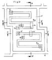
- a resistance ratio between two ion-implanted resistors R 30 and R 31 is chosen to be 1:1.
- Cross-section views taken along lines A-A', B-B' and C-C' in Figure 12 are respectively shown in Figures 13, 14 and 15.
- the two ion-implanted resistors R 30 and R 31 are formed in a bipolar monolithic IC. More particularly, formed on a P-type semiconductor substrate 50 is an N-type epitaxial layer 51, and the epitaxial layer 51 is divided into a plurality of island regions by an isolation region 52.
- the depth of these regions is 2.8 ⁇ m and the surface impurity concentration of these regions is 5x10 18 cm- 3 .
- a P-type impurity is selectively ion-implanted under the conditions of the acceleration energy of 50 KeV and the dose quantity of 1x10 13 cm- 2 and then annealed, so that ion-implanted regions 55 and 55' of the shapes shown in Figure 12 can be formed.
- the ion-implanted region 55 in the resistor R 30 extends from one contact region 53, then bends nearly at a right angle 4 times, and further is connected via the P-type region 54 to the other contact region 53.
- the P-type region 54 is provided for the purpose of allowing an interconnection conductor to pass over the resistor R 30 .
- the interconnection conductor crosses over the P-type region 54.
- the resistance of the resistor R 30 is determined by two ion-implanted regions 55-1 and 55-2. It is to be noted that the ion-implanted region 55-1 has 4 bent corners, and the ion-implanted region 55-2 has no bent corner.
- the ion-implanted region 55' in the resistor R 31 includes 4 bent corners. Hence, fluctuations in the resistance ratio caused by a difference in the number of bent corners would not arise between the resistors R 30 and R 31 .
- the resistance value of the resistor R 30 is determined by two ion-implanted regions 55-1 and 55-2, whereas that of the resistor R 31 is determined by the single ion-implanted region 55' if the region 57 is not provided, resulting in the inaccurate resistance ratio.
- a P-type region 57 formed simultaneously with the P-type regions 53, 53' and 54 is provided in a part of the ion-implanted region 55'.
- the resistance value of the resistor R 31 is determined equivalently by two ion-implanted regions 55'-1 and 55'-2.
- a fourth preferred embodiment of the present invention is illustrated in Figure 16. From viewpoint of a pattern layout, a resistor R 40 must have a rectilinear shape consisting of one ion-implanted region 60, while an ion-implanted resistor R 41 must be formed in an S-shape consisting of three ion-implanted regions 60' connected through two high concentration layers 62. Moreover, the resistance ratio R 41 /R 40 of the resistor R 41 to the resistor R 40 is desired to be equal to 1/2. Since the resistance value of the resistor R 41 is determined by the three ion-implanted regions 60', the resistance value of the resistor R 40 should be determined by six ion-implanted regions in order to obtain a precise resistance ratio.
- regions 63 and 64 are contact regions for electrodes formed simultaneously with P-type regions 61 and 62.
- the present invention is equally applicable to the case where the resistance ratio between two resistors is not an integer. For instance, let us consider the case where a precisely defined resistance ratio between an ion-implanted resistor R A (not shown) having a resistance value of 10 kohm and another ion-implanted resistor R B (not shown) having a resistance 36 kohm is to be realized. In this instance, if the number of the ion-implanted regions in the resistor R A is 2, then since a precise resistance ratio can be approximately realized by providing 7 ion-implanted regions in the resistor R e . Therefore, the resistance ratio is derived from Equation-(11) as follows:
- FIG 17 Another preferred embodiment of the present invention in the case where the intended resistance ratio between two resistors is not an integral ratio, is illustrated in Figure 17 and will be described in detail in the following.
- the resistance ratio of two resistors R 50 and R S1 is selected to be 1.75.
- the preferable shapes of the respective resistors R 50 and R 5 are shown in Figure 17.
- the resistor R 50 comprises two ion-implanted regions 60 connected to each other through a high concentration region 62, and each of the ion-implanted partial regions 60 is divided into two regions by a high concentration region 61.
- the resistor R 50 has equivalently four ion-implanted regions 60.
- the resistor R 51 comprises three ion-implanted partial regions 60' connected to each other through two high concentration regions 62', and two of the three ion-implanted partial regions 60' are divided into three regions by two high concentration regions 61
- the resistor R 5 has equivalently seven ion-implanted regions 60'.
- Equation-(11 )" it can be seen that even in the case where the desired resistance ratio is not an integral ratio, the resistance ratio can be realized at a good precision.
- the present invention by selecting the numbers of ion-implanted regions of the respective resistors so as to conform to the intended resistance ratio can be realized at a good precision regardless of the shapes of the resistors.
- the ion-implanted resistors shown in Figure 17 can be substituted for pinch resistors by regarding ion-implanted regions as P-type portions pinched between two N-type layers.
Landscapes
- Semiconductor Integrated Circuits (AREA)
Claims (6)
Applications Claiming Priority (4)
| Application Number | Priority Date | Filing Date | Title |
|---|---|---|---|
| JP80408/81 | 1981-05-27 | ||
| JP56080408A JPS57196558A (en) | 1981-05-27 | 1981-05-27 | Semiconductor integrated circuit device |
| JP56165338A JPS5867058A (ja) | 1981-10-16 | 1981-10-16 | 半導体装置 |
| JP165338/81 | 1981-10-16 |
Publications (3)
| Publication Number | Publication Date |
|---|---|
| EP0066263A1 EP0066263A1 (de) | 1982-12-08 |
| EP0066263B1 true EP0066263B1 (de) | 1986-10-01 |
| EP0066263B2 EP0066263B2 (de) | 1991-10-09 |
Family
ID=26421420
Family Applications (1)
| Application Number | Title | Priority Date | Filing Date |
|---|---|---|---|
| EP82104644A Expired EP0066263B2 (de) | 1981-05-27 | 1982-05-27 | Halbleiteranordnung mit zwei Widerständen |
Country Status (3)
| Country | Link |
|---|---|
| US (1) | US4725876A (de) |
| EP (1) | EP0066263B2 (de) |
| DE (1) | DE3273527D1 (de) |
Families Citing this family (10)
| Publication number | Priority date | Publication date | Assignee | Title |
|---|---|---|---|---|
| US5218225A (en) * | 1990-03-30 | 1993-06-08 | Dallas Semiconductor Corp. | Thin-film resistor layout |
| US5047827A (en) * | 1990-08-20 | 1991-09-10 | Hughes Aircraft Company | Integrated circuit resistor fabrication using focused ion beam |
| US5321279A (en) * | 1992-11-09 | 1994-06-14 | Texas Instruments Incorporated | Base ballasting |
| JP3244057B2 (ja) | 1998-07-16 | 2002-01-07 | 日本電気株式会社 | 基準電圧源回路 |
| US6169310B1 (en) * | 1998-12-03 | 2001-01-02 | National Semiconductor Corporation | Electrostatic discharge protection device |
| US6784747B1 (en) | 2003-03-20 | 2004-08-31 | Analog Devices, Inc. | Amplifier circuit |
| US6816015B2 (en) | 2003-03-27 | 2004-11-09 | Analog Devices, Inc. | Amplifier circuit having a plurality of first and second base resistors |
| WO2010035608A1 (en) * | 2008-09-25 | 2010-04-01 | Semiconductor Energy Laboratory Co., Ltd. | Semiconductor device and manufacturing method thereof |
| JP5677187B2 (ja) * | 2011-05-09 | 2015-02-25 | 株式会社東芝 | 半導体記憶装置 |
| US10803922B2 (en) * | 2018-09-28 | 2020-10-13 | Micron Technology, Inc. | Apparatuses and methods for internal voltage generating circuits |
Family Cites Families (6)
| Publication number | Priority date | Publication date | Assignee | Title |
|---|---|---|---|---|
| US3644802A (en) * | 1968-05-31 | 1972-02-22 | Rca Corp | Ratio-compensated resistors for integrated circuit |
| NL6907227A (de) * | 1969-05-10 | 1970-11-12 | ||
| GB1250988A (de) * | 1969-08-14 | 1971-10-27 | ||
| US3771095A (en) * | 1972-12-21 | 1973-11-06 | Ibm | Monolithic integrated circuit resistor design for optimum resistor tracking |
| US3906430A (en) * | 1974-08-29 | 1975-09-16 | Nippon Electric Co | Matrix resistors for integrated circuit |
| US4161742A (en) * | 1975-08-02 | 1979-07-17 | Ferranti Limited | Semiconductor devices with matched resistor portions |
-
1982
- 1982-05-27 DE DE8282104644T patent/DE3273527D1/de not_active Expired
- 1982-05-27 EP EP82104644A patent/EP0066263B2/de not_active Expired
-
1986
- 1986-05-15 US US06/867,422 patent/US4725876A/en not_active Expired - Lifetime
Also Published As
| Publication number | Publication date |
|---|---|
| US4725876A (en) | 1988-02-16 |
| EP0066263B2 (de) | 1991-10-09 |
| DE3273527D1 (en) | 1986-11-06 |
| EP0066263A1 (de) | 1982-12-08 |
Similar Documents
| Publication | Publication Date | Title |
|---|---|---|
| US4672314A (en) | Comprehensive semiconductor test structure | |
| EP0100571A2 (de) | Vergrabene Leistungsverbindungsstruktur niedrigen Widerstandes für integrierte Schaltungen | |
| EP0066263B2 (de) | Halbleiteranordnung mit zwei Widerständen | |
| US5567977A (en) | Precision integrated resistor | |
| GB2298086A (en) | Reduced mask process for manufacture of MOS gated devices | |
| US6305095B1 (en) | Methods and circuits for mask-alignment detection | |
| US6393714B1 (en) | Resistor arrays for mask-alignment detection | |
| US20110034010A1 (en) | Process for manufacturing a multi-drain electronic power device integrated in semiconductor substrate and corresponding device | |
| US3644802A (en) | Ratio-compensated resistors for integrated circuit | |
| EP0544364A2 (de) | Monolitische Halbleiteranordnung mit vertikaler Struktur die einen Leistungstransistor enthält mit tiefer Base und Finger-Emitter mit Ballastwiderstand | |
| AU602740B2 (en) | Wiring structure of semiconductor pressure sensor | |
| EP0282082B1 (de) | Basiszelle für eine Gatematrixvorrichtung | |
| JPH0324788B2 (de) | ||
| JPH04233754A (ja) | 集束されたイオンビームを使用する集積回路抵抗製造方法および製造された集積回路抵抗 | |
| EP0343879B1 (de) | Bipolartransistor und Verfahren zu dessen Herstellung | |
| US5204735A (en) | High-frequency semiconductor device having emitter stabilizing resistor and method of manufacturing the same | |
| US20040072398A1 (en) | Mask-alignment detection circuit in X and Y directions | |
| JPH0997876A (ja) | 半導体装置及びその製造方法 | |
| JPH0226789B2 (de) | ||
| GB2052155A (de) | ||
| JPH07111311A (ja) | 半導体装置およびその製造方法 | |
| JP2606380B2 (ja) | 半導体集積回路 | |
| JPH02268462A (ja) | 半導体装置 | |
| JPS6256666B2 (de) | ||
| JPS6320864A (ja) | 半動体装置 |
Legal Events
| Date | Code | Title | Description |
|---|---|---|---|
| PUAI | Public reference made under article 153(3) epc to a published international application that has entered the european phase |
Free format text: ORIGINAL CODE: 0009012 |
|
| AK | Designated contracting states |
Designated state(s): DE FR GB |
|
| 17P | Request for examination filed |
Effective date: 19830609 |
|
| R17P | Request for examination filed (corrected) |
Effective date: 19830608 |
|
| RAP1 | Party data changed (applicant data changed or rights of an application transferred) |
Owner name: NEC CORPORATION |
|
| GRAA | (expected) grant |
Free format text: ORIGINAL CODE: 0009210 |
|
| AK | Designated contracting states |
Kind code of ref document: B1 Designated state(s): DE FR GB |
|
| REF | Corresponds to: |
Ref document number: 3273527 Country of ref document: DE Date of ref document: 19861106 |
|
| ET | Fr: translation filed | ||
| PLBI | Opposition filed |
Free format text: ORIGINAL CODE: 0009260 |
|
| 26 | Opposition filed |
Opponent name: ROBERT BOSCH GMBH Effective date: 19870701 |
|
| PUAH | Patent maintained in amended form |
Free format text: ORIGINAL CODE: 0009272 |
|
| STAA | Information on the status of an ep patent application or granted ep patent |
Free format text: STATUS: PATENT MAINTAINED AS AMENDED |
|
| 27A | Patent maintained in amended form |
Effective date: 19911009 |
|
| AK | Designated contracting states |
Kind code of ref document: B2 Designated state(s): DE FR GB |
|
| ET3 | Fr: translation filed ** decision concerning opposition | ||
| PGFP | Annual fee paid to national office [announced via postgrant information from national office to epo] |
Ref country code: FR Payment date: 20010518 Year of fee payment: 20 |
|
| PGFP | Annual fee paid to national office [announced via postgrant information from national office to epo] |
Ref country code: DE Payment date: 20010522 Year of fee payment: 20 |
|
| PGFP | Annual fee paid to national office [announced via postgrant information from national office to epo] |
Ref country code: GB Payment date: 20010523 Year of fee payment: 20 |
|
| REG | Reference to a national code |
Ref country code: GB Ref legal event code: IF02 |
|
| PG25 | Lapsed in a contracting state [announced via postgrant information from national office to epo] |
Ref country code: GB Free format text: LAPSE BECAUSE OF EXPIRATION OF PROTECTION Effective date: 20020526 |
|
| REG | Reference to a national code |
Ref country code: GB Ref legal event code: PE20 Effective date: 20020526 |
|
| APAH | Appeal reference modified |
Free format text: ORIGINAL CODE: EPIDOSCREFNO |