EP0066295A1 - Optisches Reflektor-Fokussiergerät - Google Patents
Optisches Reflektor-Fokussiergerät Download PDFInfo
- Publication number
- EP0066295A1 EP0066295A1 EP82104828A EP82104828A EP0066295A1 EP 0066295 A1 EP0066295 A1 EP 0066295A1 EP 82104828 A EP82104828 A EP 82104828A EP 82104828 A EP82104828 A EP 82104828A EP 0066295 A1 EP0066295 A1 EP 0066295A1
- Authority
- EP
- European Patent Office
- Prior art keywords
- point source
- revolving
- symmetric axis
- point
- reflection
- Prior art date
- Legal status (The legal status is an assumption and is not a legal conclusion. Google has not performed a legal analysis and makes no representation as to the accuracy of the status listed.)
- Granted
Links
- 230000003287 optical effect Effects 0.000 title claims abstract description 41
- 238000005286 illumination Methods 0.000 description 17
- 238000010586 diagram Methods 0.000 description 10
- 238000009826 distribution Methods 0.000 description 6
- 230000004075 alteration Effects 0.000 description 5
- 238000004519 manufacturing process Methods 0.000 description 3
- 239000010453 quartz Substances 0.000 description 3
- VYPSYNLAJGMNEJ-UHFFFAOYSA-N silicon dioxide Inorganic materials O=[Si]=O VYPSYNLAJGMNEJ-UHFFFAOYSA-N 0.000 description 3
- 206010073261 Ovarian theca cell tumour Diseases 0.000 description 2
- 230000015572 biosynthetic process Effects 0.000 description 2
- 238000001514 detection method Methods 0.000 description 2
- 208000001644 thecoma Diseases 0.000 description 2
- 206010010071 Coma Diseases 0.000 description 1
- 238000013459 approach Methods 0.000 description 1
- 238000005520 cutting process Methods 0.000 description 1
- 230000007812 deficiency Effects 0.000 description 1
- 238000007599 discharging Methods 0.000 description 1
- 230000000694 effects Effects 0.000 description 1
- QSHDDOUJBYECFT-UHFFFAOYSA-N mercury Chemical compound [Hg] QSHDDOUJBYECFT-UHFFFAOYSA-N 0.000 description 1
- 229910052753 mercury Inorganic materials 0.000 description 1
- VSQYNPJPULBZKU-UHFFFAOYSA-N mercury xenon Chemical compound [Xe].[Hg] VSQYNPJPULBZKU-UHFFFAOYSA-N 0.000 description 1
- 238000000034 method Methods 0.000 description 1
- 230000000644 propagated effect Effects 0.000 description 1
- 230000005855 radiation Effects 0.000 description 1
- 239000004065 semiconductor Substances 0.000 description 1
Images



Classifications
-
- G—PHYSICS
- G03—PHOTOGRAPHY; CINEMATOGRAPHY; ANALOGOUS TECHNIQUES USING WAVES OTHER THAN OPTICAL WAVES; ELECTROGRAPHY; HOLOGRAPHY
- G03F—PHOTOMECHANICAL PRODUCTION OF TEXTURED OR PATTERNED SURFACES, e.g. FOR PRINTING, FOR PROCESSING OF SEMICONDUCTOR DEVICES; MATERIALS THEREFOR; ORIGINALS THEREFOR; APPARATUS SPECIALLY ADAPTED THEREFOR
- G03F7/00—Photomechanical, e.g. photolithographic, production of textured or patterned surfaces, e.g. printing surfaces; Materials therefor, e.g. comprising photoresists; Apparatus specially adapted therefor
- G03F7/70—Microphotolithographic exposure; Apparatus therefor
- G03F7/70216—Mask projection systems
- G03F7/70358—Scanning exposure, i.e. relative movement of patterned beam and workpiece during imaging
-
- G—PHYSICS
- G02—OPTICS
- G02B—OPTICAL ELEMENTS, SYSTEMS OR APPARATUS
- G02B19/00—Condensers, e.g. light collectors or similar non-imaging optics
- G02B19/0004—Condensers, e.g. light collectors or similar non-imaging optics characterised by the optical means employed
- G02B19/0019—Condensers, e.g. light collectors or similar non-imaging optics characterised by the optical means employed having reflective surfaces only (e.g. louvre systems, systems with multiple planar reflectors)
- G02B19/0023—Condensers, e.g. light collectors or similar non-imaging optics characterised by the optical means employed having reflective surfaces only (e.g. louvre systems, systems with multiple planar reflectors) at least one surface having optical power
-
- G—PHYSICS
- G02—OPTICS
- G02B—OPTICAL ELEMENTS, SYSTEMS OR APPARATUS
- G02B19/00—Condensers, e.g. light collectors or similar non-imaging optics
- G02B19/0033—Condensers, e.g. light collectors or similar non-imaging optics characterised by the use
- G02B19/0047—Condensers, e.g. light collectors or similar non-imaging optics characterised by the use for use with a light source
-
- G—PHYSICS
- G02—OPTICS
- G02B—OPTICAL ELEMENTS, SYSTEMS OR APPARATUS
- G02B19/00—Condensers, e.g. light collectors or similar non-imaging optics
- G02B19/0033—Condensers, e.g. light collectors or similar non-imaging optics characterised by the use
- G02B19/0095—Condensers, e.g. light collectors or similar non-imaging optics characterised by the use for use with ultraviolet radiation
Definitions
- the present invention relates to a reflection-type optical focusing apparatus which provides a light source in the shape of an arc band used in a full-size reflection-type exposing apparatus and the like.
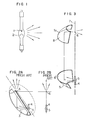
- the extra pressure mercury lamp and xenon- mercury lamp used as a point source for exposing apparatus in semiconductor fabrication are shaped as shown in Fig. 1, where reference number 1 denotes a cathode electrode and 2 denotes an anode electrode. Lamps of this type emit light by discharging, resulting in a somewhat planar light source rather than an ideal point source. Therefore, this light source is once focused at some position, then reduced to an ideal point source using a pinhole filter and the like.
- Fig. 2 shows the conventional ellipsoidal reflector
- 4 is a lamp
- 5 is the position of the point source
- 6 is the point source focusing position.
- the conventional ellipsoidal reflector 3 when provided with a larger radiation angle around the main axis, does not present a uniform light distribution around the focal point.
- the present invention is also characterized in that there are provided reflectors each shaped in a fourth-degree surface whose cross-section forms a part of an ellipse with its major axis having a certain inclination with respect to the revolving symmetric axis, on one focal point of the ellipse is located the effective point light source, thereby obtaining an arc band light source to be used in an illuminating apparatus for a full-size reflection-type exposing apparatus having a high resolution and short exposing time.
- the present invention is characterized in that there is provided the combination of at least two reflectors each shaped in a fourth-degree surface having a revolving symmetric axis formed by a line connecting the position of the point source and the position of the point source focal point, so that the effective point light source as described in the above paragraph, is obtained.
- a light source of a short wave length (deep UV) ranging 200-300 nm can be obtained by use of an Xe-Hg lamp which provides a point source, and a high resolution is achieved. Moreover, since optical transmitting components are not used, no optical loss occurs, and a light beam can be projected within a narrow band effectively.
- the most suitable optical system is the arrangement of 4th-degree surface reflectors having a revolving symmetric axis formed by a line connecting the point source position and the point source focal position, with the hightest luminance portion of the lamp being placed at the point source position.
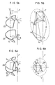
- Fourth-degree surface reflectors are classified by the shape of the cross-section which is cut on the plane including the revolving symmetric axis.
- a light beam originated from point Al reflects on surface Sl and focuses at Cl in the shape of arc, then further reflects on surface S2 and focuses at point A2, as shown in Figs. 4A and 4B.
- a light beam originated from point Al focuses at point A2 as shown in Figs. 5A and 5B.
- Reflectors having circular cross-sections generally cause the coma aberration.
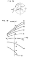
- Figure 7B shows intersections of the principal ray and a ray having an inclination of 6 with respect to the principal ray measured by displacing the center of the curvature of the circle from the revolving symmetric axis as shown in Fig. 7A.
- FIG. 8A shows the projecting ray at point Al
- Fig. 8B ellipsoidal cross-section plus ellipsoidal cross-section
- FIG. 8D shows the prior art arrangement disclosed in Japaense Patent Laid-open No. 54-123876.
- Surfaces Sl and S2 define concave mirrors 22 and 23 on 4th-degree surfaces obtained by rotating the ellipsoidal and hyperbolic cross-sections expressed by equations (2) and (3), respectively, on a plane including their revolving symmetric axis 7.
- the light source located at point Al forms an arc at point C, then it focuses at point A2 to form substantially a point.
- the projecting ray as shown in Fig. 8A results in an incident ray at point A2 as shown in Fig. 8D
- the incident ray is improved as shown in Fig. 8E (circular cross-section (with center out of the axis) plus circular cross-section (with center out of the axis)).
- the foregoing embodiments allow the formation of a clear image for realizing an ideal.point source (effective point source) by gathering the lamp energy efficiently.
- Figure 9 illustrates the optical system of the 4th-degree surface reflector.
- a line passing through the center of an arc band 12 and perpendicular to a surface S4 of the arc band is defined as a revolving symmetric axis l, and an effective point source A2 is positioned on the axis.
- a 4th-degree surface is formed such that its profile a (curve) obtained by cutting the surface on a plane S3 including the revolving symmetric axis forms an ellipse having one focal point located at the point source and another focal point at the intersection of the center line D of the arc band and the plane S3.
- a ray emitted from the effective point source A2 and propagated on the plane S3 will reflect on the profile ⁇ and will focus on the intersection I of the center line D and the plane S3. More generally, a ray emitted from point A2 and reflected on the surface ⁇ of the 4th-degree surface reflector will focus on arc D due to the fact that the surface E has its revolving symmetric axis on the line l and the center line D of the arc band has its revolving symmetric axis also on the line l.
- the effective point source A2 provides the luminous distribution extending around the arc band D due to a finite area of the light source, it illuminates the inside of the narrow arc band at a high light utilization efficiency owing to the high focusing characteristic at the point I.
- Figure 9 shows the basic arrangement of the present invention, in which an effective point source 6 is located at point A2 (focal point of ellipse ⁇ ), and the 4th-degree surface is cut to form a reflector 32 so that a ray projected to the center of the reflection surface E reflects in substantially perpendicular to the incident path.
- a diverging ray from the point source 6 reflects on the surface ⁇ and focuses on the arc slit 12.
- Figure 10 is a ray tracing diagram for a ray emitted from the center, i.e., the focal point A2, of the diverging effective point source 6 (indicated by the solid line) and a ray emitted from a point which is offset by ⁇ 0.5 mm from the point A2 (indicated by the dot and dash line).
- Fig. 11A is a ray diagram on a plane perpendicular to the arc band when the 4th-degree surface having a ellipsoidal cross-section on the plane S3 is used according to the present invention.
- the solid line, dashed line, and dot and dash line in Fig. 10 corres--pond to those in Fig. ll.
- Figures 11B and 11C are ray diagrams of the conventional reflection-type optical system, Fig. 11B using a spherical mirror, Fig. 11C using the combination of three spherical mirrors.
- Figure 11A according to the present invention shows less failure of focusing as comapred with any conventional case, and apparently a narrow area is illuminated effectively.
- Figure 12 shows the full-size reflection-type exposing apparatxs incorporating the foregoing embodiment of the present invention.
- a ray emitted from the effective point source 6 reflects on the 4th-degree surface 32 expressed by equation (5), and an arc slit illumination 12 is obtained on the mask 11.
- the ray transmitting the mask 11 reflects on the concave mirror 33 and convex mirror 34 twice and once, respectively, and projects an image pattern 36 of the arc slit on the wafer 35. Accordingly, by scanning the wafer 35 and the mask 11 at the same speed in respective directions shown by the arrows, the pattern of the mask 11 can be exposed on the entire surface of the wafer 35.
- Figure 13 shows an embodiment of the full-size reflection-type exposing apparatus according to the present invention, in which reference number 4 denotes a point source employing a Xe-Hg lamp, and 30 and 31 are concave mirrors for converging the light emitted from the point source.
- reference number 4 denotes a point source employing a Xe-Hg lamp
- 30 and 31 are concave mirrors for converging the light emitted from the point source.
- the following concave mirrors are used for the mirrors 20 and 21 shown in Fig. 4.
- the spatial relationship between the concave mirrors 20 and 21 is that they have a common revolving symmetric axis and their focal points, which are the intersections of a plane including the revolving symmetric axis and the reflection surfaces of both concave mirrors and are located out of the revolving symmetric axis, are located substantially at the same point.
- the 4th-degree surface mirrors 20 and 21 provide an effective point source at point 6.
- an arc band illumination 12 can be obtained by use of a 4th-degree surface 2 in the same wqy as in the embodiment shown in Fig. 9.
- Figure 14 is a ray digram for the illumination system fromed by the combination of three 4th-degree surfaces each having an ellipsoidal cross-section, showing the characteristics of a ray emitted from the center Al of the light source 4 in the arrangement of Fig. 13 (indicated by the solid line) and rays emitted from the points which are offset by ⁇ 0.5 mm from the center (indicated by the dashed line, and dot and dash line) on the mask 11 shown in Fig. 13.
- the figure shows that a better arc band illumination can be obtained as compared with the cases of Figs. 11B and 11C.
- concave mirrors 30 and 31 are of the type shown by 24 and 25 in Fig. 6.
- the concave mirror 25 has a revolving symmetric axis l21 passing through a light source 4, and the intersection of a plane S21 (x/z plane) including the symmetric axis and the concave mirror 25 defines a circle with its center located out of the ray axis l21. Whet the light source is located on the origin, the center of the circle is located at (x o , z o ), and the surface ⁇ of the concave mirror 25 satisfies the following 4th-degree equation.
- the concave mirror 30 is identical to that shown in Fig. 15 and has the same revolving symmetric axis.
- Fig. 16 The ray diagram on the mask surface 4 according to this embodimett is shown in Fig. 16 (the illumination ray by the illumination system formed by the combination of two 4th-degree surface each having a circular cross-section and a 4th-degree surface having an ellipsoidal cross-section).
- the figure shows that the similar or better arc band illumination 9s obtained as compared with the case of Fig. 14. It will be appreciated that light emitted from the point source 4 and traveling in directions opposite to the concave mirror 31 can be used effectively by provision of a spherical mirror 13 having its center of curvature located at the point source.
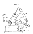
- Reference number 40 denotes the reflection-type optical focusing apparatus shown in Fig. 13, and it is mounted on a flat plate 41.
- the apparatus is provided with flat reflectors 36 and 37.
- a moving tray 42 is supported slidably by a bearing 47 on the flat plate 41.
- a means 43 for holding a mask 11 is fixed on the moving tray 42.
- An X-Y-e table 44 for mounting a wafer 35 is fixed on the moving tray 42.
- Reference number 45 denotes a driving power source for moving the tray 42, and its output is connected through a steal belt or the like 46 to the moving tray 42.
- a full-size reflection-type optical system 50 includes reflectors 51, 52 and 53, a concave spherical mirror 33 and a convex spherical mirror 34, and it is mounted on a support 48 provided on the flat plate 41.
- Reference number 54 denotes an optical detection system for registering the alignment pattern on the wafer 11 to the alignment pattern on the mask 35, In the foregoing arrangement,-the wafer 35 and the mask 11 are aligned by using the optical detection system 54, thereafter circuit patterns projected in the form of an arc band on the mask 35 by the reflection-type focusing apparatus 40 is transferred onto the wafer 11 by moving the tray 42 in a certain direction.
- the reflection-type optical focusing apparatus can be used not only for the above-mentioned full-size reflection-type exposing apparatus, but more extensively for exposing apparatus of the type where exposure is carried out by scanning the mask and wafer.
- application of the apparatus to a contact exposing apparatus and proximity exposing apparatus using ultraviolet rays or deep ultraviolet rays provides the following advanced characteristics as compared with the conventional system. It has been impossible to obtain a uniform and parallel illumination ray from a point source solely by using a reflection-type optical system, and therefore, fly-eye lens made of transmitting quartz and quartz lens have been used. However, such optical system using expensive quartz components has not provided a satisfactory uniform and parallel illumination ray.
- the illumination apparatus for exposing apparatus according to the present invention achieves a constant luminous level in any place on the arc band and also a satisfactory parallel' ray. Moreover, the illumination apparatus for exposing apparatus according to the present invention does not need transmitting optical components (by choosing the value of m in the range from 2 to 5), thereby allowing the low-cost design. This advantage is further stressed for the light having a shorter wave length for which transmitting optical components cannot be used.
- the light emitted from a point source or a light source having a small lighting area similar to the point source can be projected to a narrow area in the form of an arc band clearly, whereby only the narrow arc band pattern can be exposed onto the wafer. Therefore, only the satisfactory narrow arc band area produced by the optical projection system made u! basically of concave and convex mirrors is used to expose the wafer by scannign the mask and wafer at a high speed, and a high resolution pattern can be transferred to the wafer at a high speed.
- the present invention is very effective for improving the quality of focusing and economical condition at the same time.
Landscapes
- Physics & Mathematics (AREA)
- General Physics & Mathematics (AREA)
- Optics & Photonics (AREA)
- Exposure And Positioning Against Photoresist Photosensitive Materials (AREA)
- Lenses (AREA)
- Exposure Of Semiconductors, Excluding Electron Or Ion Beam Exposure (AREA)
- Optical Elements Other Than Lenses (AREA)
Applications Claiming Priority (4)
| Application Number | Priority Date | Filing Date | Title |
|---|---|---|---|
| JP84349/81 | 1981-06-03 | ||
| JP56084349A JPS57200012A (en) | 1981-06-03 | 1981-06-03 | Luminaire and luminaire for exposing device |
| JP84342/81 | 1981-06-03 | ||
| JP56084342A JPS57200011A (en) | 1981-06-03 | 1981-06-03 | Reflection type imaging optical device |
Publications (2)
| Publication Number | Publication Date |
|---|---|
| EP0066295A1 true EP0066295A1 (de) | 1982-12-08 |
| EP0066295B1 EP0066295B1 (de) | 1986-02-05 |
Family
ID=26425393
Family Applications (1)
| Application Number | Title | Priority Date | Filing Date |
|---|---|---|---|
| EP82104828A Expired EP0066295B1 (de) | 1981-06-03 | 1982-06-02 | Optisches Reflektor-Fokussiergerät |
Country Status (3)
| Country | Link |
|---|---|
| US (1) | US4458302A (de) |
| EP (1) | EP0066295B1 (de) |
| DE (1) | DE3268933D1 (de) |
Cited By (22)
| Publication number | Priority date | Publication date | Assignee | Title |
|---|---|---|---|---|
| GB2148525A (en) * | 1983-10-15 | 1985-05-30 | Eric Dudley | Compound parabolic reflector |
| EP0127045A3 (en) * | 1983-05-23 | 1986-10-22 | International Business Machines Corporation | Apparatus for producing a light source of required shape |
| US4765733A (en) * | 1984-10-13 | 1988-08-23 | Masataka Negishi | Light projector |
| FR2634565A1 (fr) * | 1988-07-22 | 1990-01-26 | Comp Generale Electricite | Dispositif optique de marquage par trait |
| US6438199B1 (en) | 1998-05-05 | 2002-08-20 | Carl-Zeiss-Stiftung | Illumination system particularly for microlithography |
| US6859515B2 (en) | 1998-05-05 | 2005-02-22 | Carl-Zeiss-Stiftung Trading | Illumination system, particularly for EUV lithography |
| US6858853B2 (en) | 1998-05-05 | 2005-02-22 | Carl Zeiss Smt Ag | Illumination system particularly for microlithography |
| US6859328B2 (en) | 1998-05-05 | 2005-02-22 | Carl Zeiss Semiconductor | Illumination system particularly for microlithography |
| US6947124B2 (en) | 1998-05-05 | 2005-09-20 | Carl Zeiss Smt Ag | Illumination system particularly for microlithography |
| US6947120B2 (en) | 1998-05-05 | 2005-09-20 | Carl Zeiss Smt Ag | Illumination system particularly for microlithography |
| US7071476B2 (en) | 1998-05-05 | 2006-07-04 | Carl Zeiss Smt Ag | Illumination system with a plurality of light sources |
| US7109497B2 (en) | 1998-05-05 | 2006-09-19 | Carl Zeiss Smt Ag | Illumination system particularly for microlithography |
| US7126137B2 (en) | 1998-05-05 | 2006-10-24 | Carl Zeiss Smt Ag | Illumination system with field mirrors for producing uniform scanning energy |
| US7142285B2 (en) | 1998-05-05 | 2006-11-28 | Carl Zeiss Smt Ag | Illumination system particularly for microlithography |
| US7186983B2 (en) | 1998-05-05 | 2007-03-06 | Carl Zeiss Smt Ag | Illumination system particularly for microlithography |
| US7248667B2 (en) | 1999-05-04 | 2007-07-24 | Carl Zeiss Smt Ag | Illumination system with a grating element |
| US7329886B2 (en) | 1998-05-05 | 2008-02-12 | Carl Zeiss Smt Ag | EUV illumination system having a plurality of light sources for illuminating an optical element |
| US7443948B2 (en) | 1998-05-05 | 2008-10-28 | Carl Zeiss Smt Ag | Illumination system particularly for microlithography |
| US7592598B2 (en) | 1998-05-05 | 2009-09-22 | Carl Zeiss Smt Ag | Illumination system particularly for microlithography |
| USRE41667E1 (en) * | 1998-05-05 | 2010-09-14 | Carl Zeiss Smt Ag | Illumination system particularly for microlithography |
| EP2253997A3 (de) * | 2009-05-18 | 2010-12-08 | Süss MicroTec Lithography GmbH | Beleuchtungssystem für einen mikrolithografischen Kontakt und Nähenbelichtungsvorrichtung |
| USRE42065E1 (en) | 1998-05-05 | 2011-01-25 | Carl Zeiss Smt Ag | Illumination system particularly for microlithography |
Families Citing this family (16)
| Publication number | Priority date | Publication date | Assignee | Title |
|---|---|---|---|---|
| US4681414A (en) * | 1983-06-09 | 1987-07-21 | Hershel Ronald S | Condenser system |
| US4747030A (en) * | 1986-08-13 | 1988-05-24 | The Perkin-Elmer Corporation | Illumination system |
| US4956759A (en) * | 1988-12-30 | 1990-09-11 | North American Philips Corporation | Illumination system for non-imaging reflective collector |
| US5051875A (en) * | 1990-06-01 | 1991-09-24 | Kdi American Products, Inc. | Underwater pool light |
| JPH05333268A (ja) * | 1992-06-03 | 1993-12-17 | Matsushita Electric Ind Co Ltd | 円弧照明装置 |
| US5414600A (en) * | 1993-07-30 | 1995-05-09 | Cogent Light Technologies, Inc. | Condensing and collecting optical system using an ellipsoidal reflector |
| JP2720811B2 (ja) * | 1995-03-15 | 1998-03-04 | 住友電気工業株式会社 | レーザ集光方法及び装置 |
| US5815245A (en) * | 1995-03-22 | 1998-09-29 | Etec Systems, Inc. | Scanning lithography system with opposing motion |
| JP2003506881A (ja) | 1999-07-30 | 2003-02-18 | カール ツァイス シュティフトゥング トレイディング アズ カール ツァイス | Euv照明光学系の射出瞳における照明分布の制御 |
| US6227682B1 (en) | 2000-03-22 | 2001-05-08 | Cogent Light Technologies, Inc. | Coupling of light from a small light source for projection systems using parabolic reflectors |
| DE60029442T2 (de) * | 2000-08-29 | 2007-04-19 | Perkinelmer International C.V. | Optisches System mit veränderlicher Vergrösserung |
| US6565235B2 (en) * | 2000-10-26 | 2003-05-20 | Cogent Light Technologies Inc. | Folding an arc into itself to increase the brightness of an arc lamp |
| WO2002063390A2 (en) | 2001-02-05 | 2002-08-15 | Wavien, Inc. | An illumination engine for a projection display using a tapered light pipe |
| US6856727B2 (en) * | 2001-03-02 | 2005-02-15 | Wavien, Inc. | Coupling of light from a non-circular light source |
| US6926435B2 (en) * | 2001-08-23 | 2005-08-09 | Wavien, Inc. | Led illumination engine using a reflector |
| JP2007525394A (ja) * | 2003-12-03 | 2007-09-06 | ジーイー・ヘルスケア・リミテッド | 濃縮[11c]一酸化炭素を用いるuv光による[11c]ホスゲンの合成方法及び装置 |
Citations (5)
| Publication number | Priority date | Publication date | Assignee | Title |
|---|---|---|---|---|
| US3763348A (en) * | 1972-01-05 | 1973-10-02 | Argus Eng Co | Apparatus and method for uniform illumination of a surface |
| DE2505257A1 (de) * | 1974-02-07 | 1975-08-21 | Ricoh Kk | Kondensoreinrichtung |
| US3963353A (en) * | 1974-09-26 | 1976-06-15 | The Perkin-Elmer Corporation | Monolithic beam splitter mirror arrangement |
| DE2910280A1 (de) * | 1978-03-18 | 1979-09-27 | Canon Kk | Optisches abbildungssystem |
| EP0022346A1 (de) * | 1979-07-02 | 1981-01-14 | Ealing Infra-Red Limited | Reflektorsystem mit gemeinsamem Brennpunkt |
-
1982
- 1982-06-02 DE DE8282104828T patent/DE3268933D1/de not_active Expired
- 1982-06-02 US US06/384,679 patent/US4458302A/en not_active Expired - Fee Related
- 1982-06-02 EP EP82104828A patent/EP0066295B1/de not_active Expired
Patent Citations (5)
| Publication number | Priority date | Publication date | Assignee | Title |
|---|---|---|---|---|
| US3763348A (en) * | 1972-01-05 | 1973-10-02 | Argus Eng Co | Apparatus and method for uniform illumination of a surface |
| DE2505257A1 (de) * | 1974-02-07 | 1975-08-21 | Ricoh Kk | Kondensoreinrichtung |
| US3963353A (en) * | 1974-09-26 | 1976-06-15 | The Perkin-Elmer Corporation | Monolithic beam splitter mirror arrangement |
| DE2910280A1 (de) * | 1978-03-18 | 1979-09-27 | Canon Kk | Optisches abbildungssystem |
| EP0022346A1 (de) * | 1979-07-02 | 1981-01-14 | Ealing Infra-Red Limited | Reflektorsystem mit gemeinsamem Brennpunkt |
Cited By (25)
| Publication number | Priority date | Publication date | Assignee | Title |
|---|---|---|---|---|
| EP0127045A3 (en) * | 1983-05-23 | 1986-10-22 | International Business Machines Corporation | Apparatus for producing a light source of required shape |
| GB2148525A (en) * | 1983-10-15 | 1985-05-30 | Eric Dudley | Compound parabolic reflector |
| US4765733A (en) * | 1984-10-13 | 1988-08-23 | Masataka Negishi | Light projector |
| FR2634565A1 (fr) * | 1988-07-22 | 1990-01-26 | Comp Generale Electricite | Dispositif optique de marquage par trait |
| US7126137B2 (en) | 1998-05-05 | 2006-10-24 | Carl Zeiss Smt Ag | Illumination system with field mirrors for producing uniform scanning energy |
| US7592598B2 (en) | 1998-05-05 | 2009-09-22 | Carl Zeiss Smt Ag | Illumination system particularly for microlithography |
| US6858853B2 (en) | 1998-05-05 | 2005-02-22 | Carl Zeiss Smt Ag | Illumination system particularly for microlithography |
| US6859328B2 (en) | 1998-05-05 | 2005-02-22 | Carl Zeiss Semiconductor | Illumination system particularly for microlithography |
| US6947124B2 (en) | 1998-05-05 | 2005-09-20 | Carl Zeiss Smt Ag | Illumination system particularly for microlithography |
| US6947120B2 (en) | 1998-05-05 | 2005-09-20 | Carl Zeiss Smt Ag | Illumination system particularly for microlithography |
| US7071476B2 (en) | 1998-05-05 | 2006-07-04 | Carl Zeiss Smt Ag | Illumination system with a plurality of light sources |
| US7109497B2 (en) | 1998-05-05 | 2006-09-19 | Carl Zeiss Smt Ag | Illumination system particularly for microlithography |
| US6438199B1 (en) | 1998-05-05 | 2002-08-20 | Carl-Zeiss-Stiftung | Illumination system particularly for microlithography |
| US7142285B2 (en) | 1998-05-05 | 2006-11-28 | Carl Zeiss Smt Ag | Illumination system particularly for microlithography |
| US7186983B2 (en) | 1998-05-05 | 2007-03-06 | Carl Zeiss Smt Ag | Illumination system particularly for microlithography |
| US7977651B2 (en) | 1998-05-05 | 2011-07-12 | Carl Zeiss Smt Gmbh | Illumination system particularly for microlithography |
| US7329886B2 (en) | 1998-05-05 | 2008-02-12 | Carl Zeiss Smt Ag | EUV illumination system having a plurality of light sources for illuminating an optical element |
| US7348565B2 (en) | 1998-05-05 | 2008-03-25 | Carl Zeiss Smt Ag | Illumination system particularly for microlithography |
| US7443948B2 (en) | 1998-05-05 | 2008-10-28 | Carl Zeiss Smt Ag | Illumination system particularly for microlithography |
| US7456408B2 (en) | 1998-05-05 | 2008-11-25 | Carl Zeiss Smt Ag | Illumination system particularly for microlithography |
| US6859515B2 (en) | 1998-05-05 | 2005-02-22 | Carl-Zeiss-Stiftung Trading | Illumination system, particularly for EUV lithography |
| USRE41667E1 (en) * | 1998-05-05 | 2010-09-14 | Carl Zeiss Smt Ag | Illumination system particularly for microlithography |
| USRE42065E1 (en) | 1998-05-05 | 2011-01-25 | Carl Zeiss Smt Ag | Illumination system particularly for microlithography |
| US7248667B2 (en) | 1999-05-04 | 2007-07-24 | Carl Zeiss Smt Ag | Illumination system with a grating element |
| EP2253997A3 (de) * | 2009-05-18 | 2010-12-08 | Süss MicroTec Lithography GmbH | Beleuchtungssystem für einen mikrolithografischen Kontakt und Nähenbelichtungsvorrichtung |
Also Published As
| Publication number | Publication date |
|---|---|
| US4458302A (en) | 1984-07-03 |
| EP0066295B1 (de) | 1986-02-05 |
| DE3268933D1 (en) | 1986-03-20 |
Similar Documents
| Publication | Publication Date | Title |
|---|---|---|
| EP0066295A1 (de) | Optisches Reflektor-Fokussiergerät | |
| CN1208649C (zh) | 使用双椭球反射镜将光源的光耦合到目标 | |
| US4294538A (en) | Image forming optical system | |
| US20080266650A1 (en) | Efficient EUV collector designs | |
| JPS60232552A (ja) | 照明光学系 | |
| JPS60218635A (ja) | 照明装置 | |
| JP3950553B2 (ja) | 照明光学系及びそれを有する露光装置 | |
| JPH07318847A (ja) | 照明光学装置 | |
| JPS62115719A (ja) | 照明光学系 | |
| JPS5964830A (ja) | 照明装置 | |
| KR100234357B1 (ko) | 투영노광장치 | |
| KR910001504B1 (ko) | 평행광 조명용의 광학계 | |
| JP2914035B2 (ja) | 輪帯光束形成方法および照明光学装置 | |
| JP3367569B2 (ja) | 照明光学装置、露光装置、及び該露光装置を用いた転写方法 | |
| KR0165701B1 (ko) | 조명장치 및 동장치를 사용하는 노광장치 | |
| US4400080A (en) | Two-drum type copying machine having improved illumination efficiency | |
| JPH10186673A (ja) | 露光装置 | |
| US5555135A (en) | Illumination system | |
| JPH0697047A (ja) | 照明光学系 | |
| KR0147602B1 (ko) | 콘트라스트 증대를 위한 조명 장치 | |
| JP3415879B2 (ja) | 照射装置 | |
| JP2604471B2 (ja) | 照明用光学系 | |
| JPS6219723B2 (de) | ||
| JP2957910B2 (ja) | 照明装置 | |
| JP3279090B2 (ja) | 照明装置および露光装置 |
Legal Events
| Date | Code | Title | Description |
|---|---|---|---|
| PUAI | Public reference made under article 153(3) epc to a published international application that has entered the european phase |
Free format text: ORIGINAL CODE: 0009012 |
|
| AK | Designated contracting states |
Designated state(s): DE FR NL |
|
| 17P | Request for examination filed |
Effective date: 19830502 |
|
| GRAA | (expected) grant |
Free format text: ORIGINAL CODE: 0009210 |
|
| AK | Designated contracting states |
Designated state(s): DE FR NL |
|
| REF | Corresponds to: |
Ref document number: 3268933 Country of ref document: DE Date of ref document: 19860320 |
|
| ET | Fr: translation filed | ||
| PGFP | Annual fee paid to national office [announced via postgrant information from national office to epo] |
Ref country code: NL Payment date: 19860630 Year of fee payment: 5 |
|
| PLBE | No opposition filed within time limit |
Free format text: ORIGINAL CODE: 0009261 |
|
| STAA | Information on the status of an ep patent application or granted ep patent |
Free format text: STATUS: NO OPPOSITION FILED WITHIN TIME LIMIT |
|
| 26N | No opposition filed | ||
| PG25 | Lapsed in a contracting state [announced via postgrant information from national office to epo] |
Ref country code: NL Effective date: 19880101 |
|
| NLV4 | Nl: lapsed or anulled due to non-payment of the annual fee | ||
| PG25 | Lapsed in a contracting state [announced via postgrant information from national office to epo] |
Ref country code: FR Free format text: LAPSE BECAUSE OF NON-PAYMENT OF DUE FEES Effective date: 19880226 |
|
| PG25 | Lapsed in a contracting state [announced via postgrant information from national office to epo] |
Ref country code: DE Effective date: 19880301 |
|
| REG | Reference to a national code |
Ref country code: FR Ref legal event code: ST |