EP0066404A2 - Verfahren und Vorrichtung zur Mehrkanalelektronenstrahllithographie - Google Patents
Verfahren und Vorrichtung zur Mehrkanalelektronenstrahllithographie Download PDFInfo
- Publication number
- EP0066404A2 EP0066404A2 EP82302499A EP82302499A EP0066404A2 EP 0066404 A2 EP0066404 A2 EP 0066404A2 EP 82302499 A EP82302499 A EP 82302499A EP 82302499 A EP82302499 A EP 82302499A EP 0066404 A2 EP0066404 A2 EP 0066404A2
- Authority
- EP
- European Patent Office
- Prior art keywords
- electron beam
- lenslet
- array
- target surface
- channels
- Prior art date
- Legal status (The legal status is an assumption and is not a legal conclusion. Google has not performed a legal analysis and makes no representation as to the accuracy of the status listed.)
- Granted
Links
- 238000010894 electron beam technology Methods 0.000 title claims abstract description 185
- 238000001459 lithography Methods 0.000 title claims abstract description 16
- 238000000034 method Methods 0.000 title claims description 28
- 239000004065 semiconductor Substances 0.000 claims description 36
- 238000012545 processing Methods 0.000 claims description 10
- 238000012937 correction Methods 0.000 claims description 9
- 238000013519 translation Methods 0.000 claims description 9
- 230000000712 assembly Effects 0.000 claims description 8
- 238000000429 assembly Methods 0.000 claims description 8
- 238000013507 mapping Methods 0.000 claims description 8
- 230000007246 mechanism Effects 0.000 claims description 8
- 230000001419 dependent effect Effects 0.000 claims description 7
- 230000003287 optical effect Effects 0.000 claims description 5
- 238000003780 insertion Methods 0.000 claims description 4
- 230000037431 insertion Effects 0.000 claims description 4
- 230000008878 coupling Effects 0.000 claims description 3
- 238000010168 coupling process Methods 0.000 claims description 3
- 238000005859 coupling reaction Methods 0.000 claims description 3
- 230000000694 effects Effects 0.000 claims description 2
- 238000005259 measurement Methods 0.000 claims description 2
- 230000004044 response Effects 0.000 claims description 2
- QNGNSVIICDLXHT-UHFFFAOYSA-N 4-Ethylbenzaldehyde Chemical compound CCC1=CC=C(C=O)C=C1 QNGNSVIICDLXHT-UHFFFAOYSA-N 0.000 claims 3
- 238000006073 displacement reaction Methods 0.000 claims 2
- 238000000609 electron-beam lithography Methods 0.000 claims 2
- 230000005284 excitation Effects 0.000 claims 2
- 201000009310 astigmatism Diseases 0.000 claims 1
- 238000007493 shaping process Methods 0.000 claims 1
- 230000001131 transforming effect Effects 0.000 claims 1
- 230000017105 transposition Effects 0.000 claims 1
- 235000012431 wafers Nutrition 0.000 description 44
- 238000004519 manufacturing process Methods 0.000 description 7
- XUIMIQQOPSSXEZ-UHFFFAOYSA-N Silicon Chemical compound [Si] XUIMIQQOPSSXEZ-UHFFFAOYSA-N 0.000 description 4
- 229910052710 silicon Inorganic materials 0.000 description 4
- 239000010703 silicon Substances 0.000 description 4
- 238000010586 diagram Methods 0.000 description 3
- 238000009434 installation Methods 0.000 description 3
- 238000003491 array Methods 0.000 description 2
- 238000010276 construction Methods 0.000 description 2
- 238000013461 design Methods 0.000 description 2
- 229910000831 Steel Inorganic materials 0.000 description 1
- 230000001133 acceleration Effects 0.000 description 1
- 239000012080 ambient air Substances 0.000 description 1
- 210000003323 beak Anatomy 0.000 description 1
- 230000008901 benefit Effects 0.000 description 1
- 238000004364 calculation method Methods 0.000 description 1
- 230000008859 change Effects 0.000 description 1
- 238000004590 computer program Methods 0.000 description 1
- 238000005520 cutting process Methods 0.000 description 1
- 238000011161 development Methods 0.000 description 1
- 229910052746 lanthanum Inorganic materials 0.000 description 1
- FZLIPJUXYLNCLC-UHFFFAOYSA-N lanthanum atom Chemical compound [La] FZLIPJUXYLNCLC-UHFFFAOYSA-N 0.000 description 1
- 239000000463 material Substances 0.000 description 1
- 230000000737 periodic effect Effects 0.000 description 1
- 229920002120 photoresistant polymer Polymers 0.000 description 1
- 239000010959 steel Substances 0.000 description 1
- 230000009466 transformation Effects 0.000 description 1
- WFKWXMTUELFFGS-UHFFFAOYSA-N tungsten Chemical compound [W] WFKWXMTUELFFGS-UHFFFAOYSA-N 0.000 description 1
- 229910052721 tungsten Inorganic materials 0.000 description 1
- 239000010937 tungsten Substances 0.000 description 1
Images




Classifications
-
- H—ELECTRICITY
- H01—ELECTRIC ELEMENTS
- H01J—ELECTRIC DISCHARGE TUBES OR DISCHARGE LAMPS
- H01J37/00—Discharge tubes with provision for introducing objects or material to be exposed to the discharge, e.g. for the purpose of examination or processing thereof
- H01J37/30—Electron-beam or ion-beam tubes for localised treatment of objects
- H01J37/317—Electron-beam or ion-beam tubes for localised treatment of objects for changing properties of the objects or for applying thin layers thereon, e.g. for ion implantation
- H01J37/3174—Particle-beam lithography, e.g. electron beam lithography
- H01J37/3177—Multi-beam, e.g. fly's eye, comb probe
-
- B—PERFORMING OPERATIONS; TRANSPORTING
- B82—NANOTECHNOLOGY
- B82Y—SPECIFIC USES OR APPLICATIONS OF NANOSTRUCTURES; MEASUREMENT OR ANALYSIS OF NANOSTRUCTURES; MANUFACTURE OR TREATMENT OF NANOSTRUCTURES
- B82Y10/00—Nanotechnology for information processing, storage or transmission, e.g. quantum computing or single electron logic
-
- B—PERFORMING OPERATIONS; TRANSPORTING
- B82—NANOTECHNOLOGY
- B82Y—SPECIFIC USES OR APPLICATIONS OF NANOSTRUCTURES; MEASUREMENT OR ANALYSIS OF NANOSTRUCTURES; MANUFACTURE OR TREATMENT OF NANOSTRUCTURES
- B82Y40/00—Manufacture or treatment of nanostructures
-
- H—ELECTRICITY
- H01—ELECTRIC ELEMENTS
- H01J—ELECTRIC DISCHARGE TUBES OR DISCHARGE LAMPS
- H01J37/00—Discharge tubes with provision for introducing objects or material to be exposed to the discharge, e.g. for the purpose of examination or processing thereof
- H01J37/30—Electron-beam or ion-beam tubes for localised treatment of objects
- H01J37/3002—Details
- H01J37/3007—Electron or ion-optical systems
Definitions
- This invention relates to multiple channel electron beam array lithography (EBAL) apparatus and methods of operating the same.
- EBAL electron beam array lithography
- an EBAL apparatus which employs a number of single channel electron beam columns interconnected to operate in parallel for use in the fabrication, for example, of semiconductor integrated circuits.
- each electron beam channel is contained within its own evacuated housing and requires its own mechanically movable stage for support of a target surface.
- a target surface For certain types of EBAL apparatus such an arrangement is desirable.
- the need for individual electron beam tube evacuated structures and independent target surface mechanical movement devices imposes a practical limit on the ultimate size of the apparatus both in physical space requirements and costwise.
- a multi-channel electron beam array lithography apparatus comprising: a plurality of parallel operated electron beam channels each of which are of the fly's eye type having an electron gun for producing an electron beam, an array lenslet assembly and a respective fine deflector assembly and a coarse deflector for selectively directing the electron beam to a desired array lenslet within the array lenslet assembly and its respective fine deflector which thereafter directs the electron beam to a desired point on a target surface; a common movable stage for supporting the target surface below the electron beam channels and for moving the target surface relative to all the electron beam channels; and an evacuated housing enclosing all of said electron beam channels.
- the apparatus preferably includes target position control means for automatically moving said common movable stage in a preprogrammed manner whereby substantially the entire surface area of the target surface can be brought under the combined view of the electron beam channels.
- the enlarged target surface may be the surface area of an enlarged semiconductor wafer on which a plurality of semiconductor integrated circuit chips are to be formed.
- a method of operating a multi-channel electron beam array lithography apparatus having a plurality of electron beam channels of the array optics type contained within a common evacuated housing, each of said channels comprising an electron gun for producing an electron beam, an array lenslet assembly, an array fine deflector assembly, and a coarse deflector assembly interposed between the electron gun and the array lenslet assembly for selectively directing the electron beam to a desired array lenslet of the array lenslet assembly and its respective fine deflector which directs the electron beam to a desired point on a target surface, said method comprising: operating all of said electron beam channels simultaneously in parallel in response to common pattern controlled deflection signals applied in common to the respective coarse and fine deflector assemblies of each electron beam channel thereby to write on different predetermined areas of the target surface simultaneously.
- the through-put (or productivity) of an EBAL apparatus can be increased by using multiple parallel electron beam channels of the array optics type to expose a plurality of target surfaces simultaneously.
- the disclosure will be with relation to an enlarged semiconductor wafer on which it is desired to form a plurality of semiconductor integrated circuit chips by electron beam accessed lithography.
- the description will be with relation to a semiconductor wafer; however, it is to be understood that the EBAL apparatus herein described can be employed with other target surfaces such as, for example, photoresists where it is desired to electron etch particular pattern configurations into a plurality of target surfaces simultaneously thereby to increase through-put of the EBAL apparatus with minimal cost in capital equipment.
- target surfaces such as, for example, photoresists where it is desired to electron etch particular pattern configurations into a plurality of target surfaces simultaneously thereby to increase through-put of the EBAL apparatus with minimal cost in capital equipment.
- FIG. 1 is a top plan view of a multi-channel EBAL apparatus according to the present invention having nine electron beam channels 11.
- Each electron beam channel is of the array optics type with the array optics being comprised by an assembly of 16 x 16 array lenslets and associated fine deflector elements as shown in the lowermost right hand electron beam channel.
- the channels are spaced on 3 cm (1.2 inch) centres and the array lens and deflectors of each channel cover an area of 1 cm (0.4 inch) on a side.
- the coarse deflector for each channel has a 2.5 cm (1 inch) outside diameter and an inside diameter of 1.9 cm (0.75 inch).
- Figure 1 illustrates the multi-channel EBAL apparatus in connection with a 10 cm (4 inch) diameter semiconductor wafer on which a plurality of semiconductor integrated circuit chips are to formed.
- substantially 100% efficient use of the surface area of the semiconductor wafer can be achieved by mechanically stepping the wafer position relative to the central optical axes of the electron beam channels through a 3 x 3 sub-array of channel fields.
- a channel field is meant the field of view of an electron beam channel when projected downwardly onto the target surface of the wafer.
- the geometry of the semiconductor wafer shown with the apparatus arrangement of Figure 1 imposes some restriction on the size of chips which can efficiently use the total silicon area of the wafer.
- Two constraints are involved: (1) a chip might be required to span an integral number of lenslet fields and (2) an integral number of chips must fit between the electron beam channels.
- the first constraint can be circumvented by appropriate control of the target wafer stepping coupled with lenslet stitching as described in the above-referenced European Patent Application No. 82301670.4.
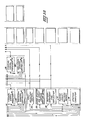
- Figure 2 is a combined schematic longitudinal sectional view of a multi-channel (EBAL) apparatus according to the present invention and functional block electric circuit diagram illustrating the essential control circuits used in conjunction with the apparatus.
- EBAL multi-channel
- Figure 2 three of the electron beam channels are shown side by side, with only one of the channels being illustrated in detail.
- a sectional view taken through the apparatus in a plane at right angles to the plane of the apparatus as shown in Figure 2 would illustrate a similar three channel assembly such that the overall apparatus is comprised of 3 x 3 or 9 electron beam channels all similarly constructed.
- the coarse deflector of electron beam channel of Figure 2 is denoted by reference numeral 11 and corresponds to one of the electron beam channels shown in the top plan view of Figure 1.
- the array of electron beam channels is supported within a common evacuated housing 12 by suitable mechanical supports not shown in Figure 2.
- Each of the electron beam channels include an electron gun composed of a cathode 13, first and second control grids 14A and 14B and an anode 15A, 15B.
- the electron gun (hereinafter referred to as 15) produces an electron beam whose path is indicated at 16 which first passes through a set of blanking electrodes 17, a first condenser lens assembly 18A, 18B, a set of spot selection electrodes 19, a second set of condenser electrodes 21A, 21B and thence to a set of steering and stigmation control electrodes 22.
- the electron beam After passing through the steering and stigmation electrodes 22, the electron beam enters the coarse deflector assembly 11 which may be constructed and operated in the manner described in United States Patent Specification No. 4 142 132. Preferably, however, the coarse deflector 11 is constructed in the manner described in European Application No. 80303974.2 (Publication No. 0 028 924). From the coarse deflector 11, the electron beam then enters a selected lenslet of an array lenslet assembly 23 which it passes through to enter an associated fine deflector element 24 which then deflects the electron beam to a desired point on a target surface supported on a movable target stage 25.
- the array lenslet assembly 23 and fine deflector assembly 24 are preferably of the type described in United States Patent Specification No. 4 200 794.
- the movable target stage 25 is designed to support on a surface 40 a target surface such as an enlarged semiconductor wafer below the fields of view of the combined 9 x 9 assembly of electron beam channels as depicted in Figure 1.
- Figure 1 shows the EBA L assembly designed for optimum use with a 10 cm (4 inch) diameter semiconductor wafer. It is to be expressly understood that the invention is in no way limited to the use of 10 cm (4 inch) diameter wafers but could be used with 12.7 cm (5 inch) or 15.2 cm (6 inch) or any other diameter wafer by appropriate design and spacing between the electron beam channels. The spacing between channels would, of course, be such as to optimize efficient use of the surface of the semiconductor wafer.
- the enlarged semiconductor wafer target surface is supported on the target stage 25 which is movably positioned within the evacuated housing 12 beneath the field of view of the 3 x 3 array of electron beam channels.
- the target stage 25 is mechanically coupled to an x-y stage translation mechanism 26 of conventional, commercially available construction through a vacuum type flexible coupling 27.
- the x-y stage translation mechanism 26 in turn, is electrically controlled by a movable stage position control circuit 28 that, in turn, comes under the control of a station computer 29.
- the station computer 29 can be preprogrammed to cause the control circuit 28 to have the x-y stage translation mechanism 26 controllably step the target stage 25 along either the x or X axis of a plane that is normal to the plane of Figure 2 and substantially normal to the electron beam paths of the electron beam channels.
- the target stage 25 can be caused to move the enlarged target wafer as shown in Figure 1 either right or left-or ⁇ p or down so as to move the 3 x 3 sub-array of channel fields selectively beneath all of the electron beam channels simultaneously.
- the channel field of the 9 electron beam channels corresponding to the field which is shown in cross hatch to illustrate the 16 x 16 array lenslet and deflector fields of view would be centred under the respective electron beam channels in the manner shown. Thereafter, in a preprogrammed manner, the semiconductor wafer would be moved by the target stage 25 for a distance corresponding to the centre-to- centre spacing of the 3 x 3 sub-array of channel fields so as to bring, for example, the next channel field to the right of those illustrated beneath the field of view of the respective electron beam channels.
- the semiconductor wafer would be stepped through all of the 3 x 3 sub-array of channel fields by the station computer 29 via the control circuit 28 and the x-y stage translation mechanism 26, the flexible vacuum tight coupling 27 and target stage 25 in accordance with preprogrammed lithography processing steps and patterns so as to cover substantially the entire surface area of the semiconductor wafer by the combined fields of view of all of the parallel operated electron beam channels used in conjunction with the mechanical stepping of the target surface.
- Each of the 3 x 3 array of electron beam channels shown in Figure 2 should employ a cathode which combines adequate brightness and low operating temperature with long life in a demountable vacuum chamber which may be occasionally exposed to ambient air.
- the cathode should be designed for periodic replacement in demountable hardware.
- One suitable cathode would be tungsten having a brightness of approximately 3 x 10 4 amperes per square centimetre per sterradin.
- An even better choice having higher brightness would be a lanthanum hexaboride cathode which could operate the EBAL apparatus at a brightness of about 4 x 1 0 5 amperes per square centimetre per sterradin.
- the cathode and electron gun of each of the electron beam channels is supplied from a high voltage and cathode power supply 31.
- the beak blanker electrodes 17 are supplied from an electron beam blanker control circuit 32, the condenser lens assembly 18 and the condensor electrodes 21 are maintained at ground potential and the beam spot size and the shape selection electrode 19 is under the control of a spot selection control circuit 33.
- the steering and stigmation control electrodes 22 are controlled by a steering and stigmation control circuit 34 and the coarse deflector 11A is under the control of a coarse deflector control circuit 35.
- the array lenslet assembly 23 are under the control of a channel array lens control circuit 36, the fine deflector assembly 24 under the control of associated fine deflection correction circuit 37 as well as a pattern dependent fine deflection control circuit 38 shown on the right hand side of Figure 2.
- Fiducial signal processing circuits for each of the electron beam channels are shown at 39, and lastly a flawed lenslet pattern memory circuit 41 which works in conjunction with the station computer 29 and controllers 30.
- control and supply circuits shown on the right hand side of Figure 2 are common to all of the electron beam channels. These are composed of the high voltage and cathode power supply 31, the spot selection control circuit 33, the coarse deflection control circuit 35, the flawed lenslet pattern memory 41, the station computer 29, the pattern dependent fine control circuit 38 and the movable stage position control circuit 28.
- the control circuits shown on the left hand side of Figure 2 are independently controlled by the individual channel controllers 30 for operation in conformance with the operating characteristics of each of the individual electron beam channels. These are composed of the blanker control circuits 32, the individual channel controllers 30, the steering and stigmation control circuit 34, the channel array lens control circuit 36, the fine deflection correction circuit 37 and the fiducial signal processing circuits 39.
- a chip registration grid is defined by first producing fiducial marking holes at the corners of each integrated circuit chip in the manner described in European Application No. 82301670.4.
- the next problem which has to be considered in the subject apparatus is any inaccuracy in lenslet stitching and the pattern registration which can occur due to the non-orthogonal angle which the electron beams make at the target surface due to the fact that exposure to the electron beams is made on the surface of workpieces which are not inserted at exactly the same height (distance from the electron source) as the original lenslet stitching calibration grid employed to form the chip registration grid.
- This problem is explained more fully in the above-mentioned European Application No. 82301670.4, and reference is made to that application for a more detailed description of the problem and the manner in which it is overcome by appropriate correction.
- the flawed lenslet problem can be solved by permuting a semiconductor target wafer between two stations in a manner such that any portion of a target surface which previously had been exposed to the field of view of a flawed lenslet, is selectively and in a program controlled manner permuted to a new position where it is subjected to the field of view of a good lenslet and the target then subsequently exposed to the electron beam in accordance with the pattern movement of the beam required for that particular area of the target.
- the manner in which permutation of the target wafers between two positions to correct for the existence of any flawed lenslets again is described more fully in the above-mentioned European Application No. 82301670.4, and reference is made to that application for a full description of the techniques required.
- the electron beams produced by the electron gun of each of the 9 electron beam channels first passes through the set of blanking electrodes 17, which are positioned to deflect the electron beam off an aperture and onto an opaque plate for cutting off or blanking the beam of each channel before it reaches the target surface.
- blanking is discontinued, and the individual electron beams are allowed to pass through the beam spot selection electrodes 19 for establishing the size and shape of the electron beam spot.
- the beam then passes through the steering and stigmation control electrodes 22 for aligning the electron beam with the axis of the coarse deflector 11A for deflecting the electron beam 16 to the entrance of a particular lenslet in the array lenslet assembly 23. Because the coarse deflectors 11A of all of the electron beam channels are under the common control of the coarse deflection control circuit 35, the electron beams of all of the electron beam channels will be deflected to corresponding ones of an array lenslet in the array lenslet assemblies. After passing through the array lenslet assembly, the electron beams will pass through corresponding associated ones of the fine deflectors which likewise are under the common control of the pattern dependent fine deflection control circuit 38.
- the through-put of the multiple channel EBAL apparatus shown and described with relation to Figures 1 and 2 is determined primarily by three factors: exposure time, wafer positioning time between exposure fields and mechanical transport time to and from the exposure station. Table II - below lists these factors with relation to the stepping rate of a single channel EBAL apparatus so that the stepping rate for a 9 channel EBAL apparatus can be obtained by multiplying the number of channels times the assumed stepping rate of 20 MHz at which a single channel of the apparatus is designed to operate.
- FIG. 4 The relationship between resolution, exposure time, and beam stepping rate is depicted in Figure 4 where the stepping rate is calculated on the basis of a single channel EBAL apparatus.
- a stepping rate of 20 MHz is designed into the 9 channel EBAL apparatus shown in Figure 2 for each electron beam channel so that an equivalent rate of 180 MHz is obtained for the overall E B AL apparatus. From Figure 4 it will be seen that for an exposure time of 0.50 minutes for a minimum feature size of 0.5 microns, this value of exposure time is entered in Table II to obtain the total time which is required in the processing of a single chip by a single channel EBAL apparatus.
- T-lC thermal cathode-single channel
- the stepping rate of the writing electron beam spot must fall within a practical range.
- the relationship between the smallest feature and the smallest electron beam spot obtainable must be clearly defined. It is assumed that these are equal if the spot profile is sharp; however, for a Gaussian profile, the smallest feature is 3 to 4 times spot diameter in size. In Figure 4 it is assumed that the profile is sharp and, therefore, that the smallest feature and the smallest spot are equal.
- the stepping rates corresponding to 10% coverage of the smallest feature are obtained from the nomograph superimposed on Figure 4. These rates have been calculated by neglecting the time required for 15% coverage with the largest spot (feature).
- the multi-channel EBAL apparatus be capable of processing integrated circuit chips wherein the smallest feature falls between O.5 and 0.75 microns.
- the apparatus has an exposure time of 0.5 to 1 minute for integrated circuit chips processed on 10 cm (4-inch) semiconductor wafers.
- the cross-hatched nomograph area in Figure 4 depicts these operating characteristics. Within the framework of the assumptions used in developing Figure 4, such a range of operations appears to be unaccessible to EBAL apparatus which employ thermal emitters but is fully within the capability of EBAL apparatus employing field emitters. In such EBAL apparatus, the electron beam stepping frequency is seen to be from approximately 30 to 100 MHz for a single channel EBAL apparatus.
- the movable stage motion in order to calculate the time required for wafer positioning, the movable stage motion must be considered. This motion is subject to three design constraints; accuracy, speed and stability. Because the need for extremely accurate absolute positioning is reduced by-the use of computer correction, via the fiducial marking signals, the x-y stage translation mechanism 26 is not limited by instrumentation requirements such as pulse-counting. However, as speed is increased, the locally dissipated energy increases rapidly, adding to the thermal stability problem.
- Table II shows the projected through-put of fabrication of semiconductor integrated circuit chips on 10 cm (4 inch) target wafers to be of the order of 51 target wafers per hour.
- each station comprises a multiple channel EBAL apparatus of the type shown in Figures 1 and 2, and where all of the stations are operated in parallel under the supervision of a system executive computer.
- the economic advantage of such multiple, multi-channel EBAL apparatus in an increased capacity system results from a significant sharing of the vacuum systems, the transport system for the target wafers and the electronic hardware as shown in Figures 3A and 3B of the drawings.
- a multistation EBAL apparatus according to the present invention is shown where there are from 1 to N stations where N is a number determined by the desired through-put of the overall EBAL apparatus.
- each electron beam channel also will have supplied to it control signals from a spot selection control circuit 33, a coarse deflection control circuit 35, a pattern dependent fine deflection circuit 38 and a flawed lenslet pattern memory 41 all of which are shared in common through the station computer 29 with other electron beam channels in the station. Since all stations would be fabricated in the same manner, a description of other channels in the station or for that matter description of the other stations is deemed unnecessary.
- the station computers of all of the stations are under the control of a master system executive computer 44 which serves all of the stations. It is assumed that all of the stations will be fabricating a mass produced semiconductor integrated circuit chip hence a master complete pattern memory 42 can be provided at the system executive computer 44 for controlling all of the stations which in turn control all of the electron beam channels. This also makes it possible for the system installation to have a single master control circuit 28 and a single master power supply 31 supplying all of the channels of all of the stations thereby to economize on the hardware required in the overall EBAL apparatus.
- a second natural integrated circuit chip size which would be convenient would be to make the chip size commensurate with the size of the field of view of the electron beam channels. This constraint would result in the simplest of chip fiducial marking signal grid fabrication, calibration grid and chip registration grid fabrication and would result in the minimum number of mechanical steps for the movable target stage. Examples of various other relationships between the integrated circuit chip size and the size of the fields of view of the electron beam channels are illustrated in Figure 5.
- Figure 5B illustrates a situation wherein the semiconductor integrated circuit chip size exceeds the size of the field of view of the electron beam channels in one dimension only.
- the fiducial holes are chosen such that only 3 x 3 mechanical steps are required along the long dimension but more steps are required along the short dimension similar to Figure 5A. Another requirement is that placement of fiducial holes within the working edge of the chip would be required.
- Figure 5C illustrates a situation where the integrated circuit chips are larger than the channel field of view in both dimensions. In this situation it may be possible to write the target wafer with only 3 x 3 movement; however, the wafer can only be written by placing fiducial holes within the working area of the chips.
- the outer electron beam channels 11 surrounding a centre channel 11C are moved in and out radially from a common centre position by means of lead screws 51 which are simultaneously turned by means of a rack and pinion 52 supported on suitable bearing blocks 53. All of the rack and pinions 52 and hence lead screws 51 are moved simultaneously by rotating a ring-shaped rack 54 by a column positioning drive motor 55 under the control of a column drive motor controller 56.
- the column drive motor controller 56 would be included along with the common stations controls in the EBAL apparatus of Figure 2 or Figure 3A and 3B.
- the electron beam channels can be moved in and out so as to maintain a regular rectangular array while providing variable spacing between the centres of the electron beam columns.
- a differential screw arrangement would be required in order to provide the required position movement of the electron beam channels.
- the accuracy of movement required is determined by the electronic capture range of the fiducial marking signal deriving system which is known to be in the order of 0.03 mm to 0.1 mm '(I to 3 mils). Also,it should be noted that movement of the electron beam channels does not occur very often (only when it is necessary to adapt the installation to a new and different size integrated circuit chip) and thus the movement can be effected at slow speeds. Hence, a digital stepping motor inside the evacuated housing 12 and under the control of the same computer program which writes patterns on the chips could be used.
Landscapes
- Engineering & Computer Science (AREA)
- Chemical & Material Sciences (AREA)
- Nanotechnology (AREA)
- Crystallography & Structural Chemistry (AREA)
- Physics & Mathematics (AREA)
- Analytical Chemistry (AREA)
- Mathematical Physics (AREA)
- Theoretical Computer Science (AREA)
- Condensed Matter Physics & Semiconductors (AREA)
- General Physics & Mathematics (AREA)
- Manufacturing & Machinery (AREA)
- Electron Beam Exposure (AREA)
- Exposure And Positioning Against Photoresist Photosensitive Materials (AREA)
Applications Claiming Priority (2)
| Application Number | Priority Date | Filing Date | Title |
|---|---|---|---|
| US06/266,074 US4390789A (en) | 1981-05-21 | 1981-05-21 | Electron beam array lithography system employing multiple parallel array optics channels and method of operation |
| US266074 | 1981-05-21 |
Publications (3)
| Publication Number | Publication Date |
|---|---|
| EP0066404A2 true EP0066404A2 (de) | 1982-12-08 |
| EP0066404A3 EP0066404A3 (en) | 1984-01-04 |
| EP0066404B1 EP0066404B1 (de) | 1986-12-30 |
Family
ID=23013057
Family Applications (1)
| Application Number | Title | Priority Date | Filing Date |
|---|---|---|---|
| EP82302499A Expired EP0066404B1 (de) | 1981-05-21 | 1982-05-17 | Verfahren und Vorrichtung zur Mehrkanalelektronenstrahllithographie |
Country Status (6)
| Country | Link |
|---|---|
| US (1) | US4390789A (de) |
| EP (1) | EP0066404B1 (de) |
| JP (1) | JPS5825235A (de) |
| AU (1) | AU547244B2 (de) |
| CA (1) | CA1186067A (de) |
| DE (1) | DE3274922D1 (de) |
Cited By (5)
| Publication number | Priority date | Publication date | Assignee | Title |
|---|---|---|---|---|
| EP0220668A3 (en) * | 1985-10-25 | 1989-01-11 | Hitachi, Ltd. | Charged particle beam lithography system |
| GB2224289A (en) * | 1988-09-06 | 1990-05-02 | Zeiss Stiftung | Plasma coating process |
| GB2337359A (en) * | 1998-05-12 | 1999-11-17 | Advantest Corp | Electron-beam lithography system |
| GB2339070A (en) * | 1998-07-02 | 2000-01-12 | Advantest Corp | Charged particle beam exposure apparatus |
| US6344655B1 (en) | 1998-07-17 | 2002-02-05 | Advantest Corporation | Multicolumn charged-particle beam lithography system |
Families Citing this family (39)
| Publication number | Priority date | Publication date | Assignee | Title |
|---|---|---|---|---|
| US4465934A (en) * | 1981-01-23 | 1984-08-14 | Veeco Instruments Inc. | Parallel charged particle beam exposure system |
| USRE33931E (en) * | 1981-12-21 | 1992-05-19 | American Semiconductor Equipment Technologies | Laser pattern generating system |
| US4694178A (en) * | 1985-06-28 | 1987-09-15 | Control Data Corporation | Multiple channel electron beam optical column lithography system and method of operation |
| US4718019A (en) * | 1985-06-28 | 1988-01-05 | Control Data Corporation | Election beam exposure system and an apparatus for carrying out a pattern unwinder |
| JPS6257215A (ja) * | 1985-09-06 | 1987-03-12 | Jeol Ltd | 荷電粒子ビ−ム描画装置 |
| US4668080A (en) * | 1985-11-29 | 1987-05-26 | Rca Corporation | Method and apparatus for forming large area high resolution patterns |
| US4945246A (en) * | 1989-03-24 | 1990-07-31 | International Business Machines Corporation | Tri-deflection electron beam system |
| US4966787A (en) * | 1989-06-19 | 1990-10-30 | The Perkin Elmer Corporation | Method of creating isolated plates on the inside surface of a metallized substrate |
| US5043586A (en) * | 1990-10-25 | 1991-08-27 | International Business Machines Corporation | Planarized, reusable calibration grids |
| US5169488A (en) * | 1990-10-25 | 1992-12-08 | International Business Machines Corporation | Method of forming planarized, reusable calibration grids |
| US5384463A (en) * | 1991-06-10 | 1995-01-24 | Fujisu Limited | Pattern inspection apparatus and electron beam apparatus |
| US5548625A (en) * | 1995-03-02 | 1996-08-20 | Motorola, Inc. | Method for parallel multiple field processing in X-ray lithography |
| JP3400601B2 (ja) * | 1995-04-06 | 2003-04-28 | 富士通株式会社 | 荷電粒子ビーム露光方法及び装置 |
| US6122562A (en) * | 1997-05-05 | 2000-09-19 | Applied Materials, Inc. | Method and apparatus for selectively marking a semiconductor wafer |
| US6104035A (en) * | 1997-06-02 | 2000-08-15 | Canon Kabushiki Kaisha | Electron-beam exposure apparatus and method |
| US6124140A (en) * | 1998-05-22 | 2000-09-26 | Micron Technology, Inc. | Method for measuring features of a semiconductor device |
| US7345290B2 (en) * | 1999-10-07 | 2008-03-18 | Agere Systems Inc | Lens array for electron beam lithography tool |
| US6355994B1 (en) * | 1999-11-05 | 2002-03-12 | Multibeam Systems, Inc. | Precision stage |
| WO2001039243A1 (en) * | 1999-11-23 | 2001-05-31 | Ion Diagnostics, Inc. | Electron optics for multi-beam electron beam lithography tool |
| WO2001059805A1 (en) | 2000-02-09 | 2001-08-16 | Fei Company | Multi-column fib for nanofabrication applications |
| JP2003524867A (ja) * | 2000-02-09 | 2003-08-19 | エフ・イ−・アイ・カンパニー | 集束イオンビームシステムのための二次粒子のレンズ通過捕捉 |
| US6943351B2 (en) * | 2000-02-19 | 2005-09-13 | Multibeam Systems, Inc. | Multi-column charged particle optics assembly |
| US6734428B2 (en) | 2000-02-19 | 2004-05-11 | Multibeam Systems, Inc. | Multi-beam multi-column electron beam inspection system |
| WO2001060456A1 (en) | 2000-02-19 | 2001-08-23 | Ion Diagnostics, Inc. | Multi-beam multi-column electron beam inspection system |
| US6787780B2 (en) * | 2000-04-04 | 2004-09-07 | Advantest Corporation | Multi-beam exposure apparatus using a multi-axis electron lens, fabrication method of a semiconductor device |
| US20030048427A1 (en) * | 2001-01-31 | 2003-03-13 | Applied Materials, Inc. | Electron beam lithography system having improved electron gun |
| US6797953B2 (en) | 2001-02-23 | 2004-09-28 | Fei Company | Electron beam system using multiple electron beams |
| US7122795B2 (en) * | 2001-04-18 | 2006-10-17 | Multibeam Systems, Inc. | Detector optics for charged particle beam inspection system |
| US7446474B2 (en) * | 2002-10-10 | 2008-11-04 | Applied Materials, Inc. | Hetero-junction electron emitter with Group III nitride and activated alkali halide |
| US7161162B2 (en) * | 2002-10-10 | 2007-01-09 | Applied Materials, Inc. | Electron beam pattern generator with photocathode comprising low work function cesium halide |
| US7015467B2 (en) * | 2002-10-10 | 2006-03-21 | Applied Materials, Inc. | Generating electrons with an activated photocathode |
| US6803582B2 (en) * | 2002-11-29 | 2004-10-12 | Oregon Health & Science University | One dimensional beam blanker array |
| WO2007015615A1 (en) * | 2005-07-30 | 2007-02-08 | Cebt Co. Ltd. | Inspection equipment for fine pattern and morphology using microcolumn |
| US9305747B2 (en) * | 2010-11-13 | 2016-04-05 | Mapper Lithography Ip B.V. | Data path for lithography apparatus |
| JP5662863B2 (ja) * | 2011-03-31 | 2015-02-04 | 株式会社ニューフレアテクノロジー | 荷電粒子ビーム描画装置及び荷電粒子ビーム描画方法 |
| JP7026502B2 (ja) * | 2017-12-26 | 2022-02-28 | 株式会社ニューフレアテクノロジー | 荷電粒子ビーム描画装置 |
| US10438769B1 (en) * | 2018-05-02 | 2019-10-08 | Kla-Tencor Corporation | Array-based characterization tool |
| KR102731121B1 (ko) * | 2019-04-18 | 2024-11-18 | 삼성디스플레이 주식회사 | 렌즈 모듈 및 이를 포함한 기판 절단 장치 |
| US11899375B2 (en) | 2020-11-20 | 2024-02-13 | Kla Corporation | Massive overlay metrology sampling with multiple measurement columns |
Family Cites Families (9)
| Publication number | Priority date | Publication date | Assignee | Title |
|---|---|---|---|---|
| JPS5116754B1 (de) * | 1970-03-04 | 1976-05-27 | ||
| JPS52109373A (en) * | 1976-03-10 | 1977-09-13 | Rikagaku Kenkyusho | Method of deflecting and scanning electron beam |
| JPS52119178A (en) * | 1976-03-31 | 1977-10-06 | Toshiba Corp | Electron beam exposure device |
| US4097745A (en) * | 1976-10-13 | 1978-06-27 | General Electric Company | High resolution matrix lens electron optical system |
| US4142132A (en) * | 1977-07-05 | 1979-02-27 | Control Data Corporation | Method and means for dynamic correction of electrostatic deflector for electron beam tube |
| JPS5463681A (en) * | 1977-10-29 | 1979-05-22 | Nippon Aviotronics Kk | Electron beam exposure device |
| JPS54160177A (en) * | 1978-06-09 | 1979-12-18 | Toshiba Corp | Electron beam exposure device |
| US4200794A (en) * | 1978-11-08 | 1980-04-29 | Control Data Corporation | Micro lens array and micro deflector assembly for fly's eye electron beam tubes using silicon components and techniques of fabrication and assembly |
| US4354111A (en) * | 1981-03-10 | 1982-10-12 | Veeco Instruments Incorporated | Screen lens array system |
-
1981
- 1981-05-21 US US06/266,074 patent/US4390789A/en not_active Expired - Lifetime
-
1982
- 1982-05-17 DE DE8282302499T patent/DE3274922D1/de not_active Expired
- 1982-05-17 EP EP82302499A patent/EP0066404B1/de not_active Expired
- 1982-05-20 CA CA000403363A patent/CA1186067A/en not_active Expired
- 1982-05-20 JP JP57085665A patent/JPS5825235A/ja active Pending
- 1982-05-20 AU AU84001/82A patent/AU547244B2/en not_active Ceased
Cited By (10)
| Publication number | Priority date | Publication date | Assignee | Title |
|---|---|---|---|---|
| EP0220668A3 (en) * | 1985-10-25 | 1989-01-11 | Hitachi, Ltd. | Charged particle beam lithography system |
| GB2224289A (en) * | 1988-09-06 | 1990-05-02 | Zeiss Stiftung | Plasma coating process |
| GB2224289B (en) * | 1988-09-06 | 1992-11-04 | Zeiss Stiftung | Plasma coating process |
| GB2337359A (en) * | 1998-05-12 | 1999-11-17 | Advantest Corp | Electron-beam lithography system |
| GB2337359B (en) * | 1998-05-12 | 2000-06-28 | Advantest Corp | Electron-beam lithography system |
| GB2339070A (en) * | 1998-07-02 | 2000-01-12 | Advantest Corp | Charged particle beam exposure apparatus |
| GB2339070B (en) * | 1998-07-02 | 2000-07-26 | Advantest Corp | Charged particle beam exposure apparatus |
| US6407397B1 (en) | 1998-07-02 | 2002-06-18 | Advantest Corporation | Charged particle beam exposure apparatus |
| US6344655B1 (en) | 1998-07-17 | 2002-02-05 | Advantest Corporation | Multicolumn charged-particle beam lithography system |
| DE19934049C2 (de) * | 1998-07-17 | 2002-06-13 | Advantest Corp | Multikolonnen-Lithographiesystem mit geladenem Teilchenstrahl |
Also Published As
| Publication number | Publication date |
|---|---|
| EP0066404A3 (en) | 1984-01-04 |
| AU547244B2 (en) | 1985-10-10 |
| EP0066404B1 (de) | 1986-12-30 |
| AU8400182A (en) | 1982-11-25 |
| CA1186067A (en) | 1985-04-23 |
| JPS5825235A (ja) | 1983-02-15 |
| DE3274922D1 (en) | 1987-02-05 |
| US4390789A (en) | 1983-06-28 |
Similar Documents
| Publication | Publication Date | Title |
|---|---|---|
| EP0066404B1 (de) | Verfahren und Vorrichtung zur Mehrkanalelektronenstrahllithographie | |
| US4694178A (en) | Multiple channel electron beam optical column lithography system and method of operation | |
| EP0063429B1 (de) | Elektronenstrahlmatrix-Lithographiegerät und Verwendungsverfahren desselben | |
| US4467211A (en) | Method and apparatus for exposing multi-level registered patterns interchangeably between stations of a multi-station electron-beam array lithography (EBAL) system | |
| US6777697B2 (en) | Charged-particle beam exposure apparatus and device manufacturing method using the same | |
| JP3478058B2 (ja) | 荷電粒子線描画装置 | |
| US4465934A (en) | Parallel charged particle beam exposure system | |
| US3875416A (en) | Methods and apparatus for the production of semiconductor devices by electron-beam patterning and devices produced thereby | |
| US4494004A (en) | Electron beam system | |
| KR102410976B1 (ko) | 멀티 하전 입자 빔 묘화 장치 및 멀티 하전 입자 빔 묘화 방법 | |
| GB2349737A (en) | Electron beam exposure apparatus | |
| EP0289279B1 (de) | Musteraufzeichnungsgerät mit Mehrfach-Elektronenstrahl | |
| US5254417A (en) | Reflection mask and electrically charged beam exposing apparatus using the reflection mask | |
| US5012105A (en) | Multiple-imaging charged particle-beam exposure system | |
| US3736425A (en) | Screen for ion implantation | |
| US6218060B1 (en) | Electron beam exposure method and electron beam exposure apparatus | |
| JP2019114731A (ja) | マルチ荷電粒子ビーム描画装置及びマルチ荷電粒子ビーム描画方法 | |
| JPH07192682A (ja) | 多重電子ビーム照射装置および照射方法 | |
| US4393312A (en) | Variable-spot scanning in an electron beam exposure system | |
| US4354111A (en) | Screen lens array system | |
| US3857041A (en) | Electron beam patterning system for use in production of semiconductor devices | |
| EP0434990B1 (de) | Verfahren und Gerät zur Belichtung mittels eines Ladungsträgerstrahls | |
| EP0035556B1 (de) | Elektronenstrahlsystem | |
| US5349197A (en) | Method for exposing a pattern on an object by a charged particle beam | |
| EP0074238B1 (de) | Belichtungsverfahren unter Benützung eines Energiestrahls |
Legal Events
| Date | Code | Title | Description |
|---|---|---|---|
| PUAI | Public reference made under article 153(3) epc to a published international application that has entered the european phase |
Free format text: ORIGINAL CODE: 0009012 |
|
| AK | Designated contracting states |
Designated state(s): DE FR GB |
|
| PUAL | Search report despatched |
Free format text: ORIGINAL CODE: 0009013 |
|
| AK | Designated contracting states |
Designated state(s): DE FR GB |
|
| 17P | Request for examination filed |
Effective date: 19840604 |
|
| GRAA | (expected) grant |
Free format text: ORIGINAL CODE: 0009210 |
|
| AK | Designated contracting states |
Kind code of ref document: B1 Designated state(s): DE FR GB |
|
| REF | Corresponds to: |
Ref document number: 3274922 Country of ref document: DE Date of ref document: 19870205 |
|
| ET | Fr: translation filed | ||
| PLBE | No opposition filed within time limit |
Free format text: ORIGINAL CODE: 0009261 |
|
| STAA | Information on the status of an ep patent application or granted ep patent |
Free format text: STATUS: NO OPPOSITION FILED WITHIN TIME LIMIT |
|
| 26N | No opposition filed | ||
| PGFP | Annual fee paid to national office [announced via postgrant information from national office to epo] |
Ref country code: GB Payment date: 19900418 Year of fee payment: 9 |
|
| PGFP | Annual fee paid to national office [announced via postgrant information from national office to epo] |
Ref country code: FR Payment date: 19900423 Year of fee payment: 9 |
|
| PGFP | Annual fee paid to national office [announced via postgrant information from national office to epo] |
Ref country code: DE Payment date: 19900426 Year of fee payment: 9 |
|
| PG25 | Lapsed in a contracting state [announced via postgrant information from national office to epo] |
Ref country code: GB Effective date: 19910517 |
|
| GBPC | Gb: european patent ceased through non-payment of renewal fee | ||
| PG25 | Lapsed in a contracting state [announced via postgrant information from national office to epo] |
Ref country code: FR Effective date: 19920131 |
|
| PG25 | Lapsed in a contracting state [announced via postgrant information from national office to epo] |
Ref country code: DE Effective date: 19920303 |
|
| REG | Reference to a national code |
Ref country code: FR Ref legal event code: ST |