EP0066487B1 - Datenübertragungssystem und in diesem System verwendete Sende- und Empfangsausrüstung - Google Patents
Datenübertragungssystem und in diesem System verwendete Sende- und Empfangsausrüstung Download PDFInfo
- Publication number
- EP0066487B1 EP0066487B1 EP82400832A EP82400832A EP0066487B1 EP 0066487 B1 EP0066487 B1 EP 0066487B1 EP 82400832 A EP82400832 A EP 82400832A EP 82400832 A EP82400832 A EP 82400832A EP 0066487 B1 EP0066487 B1 EP 0066487B1
- Authority
- EP
- European Patent Office
- Prior art keywords
- data
- output
- circuit
- input
- gate
- Prior art date
- Legal status (The legal status is an assumption and is not a legal conclusion. Google has not performed a legal analysis and makes no representation as to the accuracy of the status listed.)
- Expired
Links
- 230000005540 biological transmission Effects 0.000 title claims description 29
- 238000012937 correction Methods 0.000 claims description 9
- 230000005764 inhibitory process Effects 0.000 claims description 8
- 238000010586 diagram Methods 0.000 description 7
- 238000010200 validation analysis Methods 0.000 description 3
- 238000004088 simulation Methods 0.000 description 2
- 238000009792 diffusion process Methods 0.000 description 1
- 230000000694 effects Effects 0.000 description 1
- 230000006870 function Effects 0.000 description 1
- 238000012986 modification Methods 0.000 description 1
- 230000004048 modification Effects 0.000 description 1
- 238000005457 optimization Methods 0.000 description 1
- 230000000717 retained effect Effects 0.000 description 1
Images


Classifications
-
- H—ELECTRICITY
- H04—ELECTRIC COMMUNICATION TECHNIQUE
- H04J—MULTIPLEX COMMUNICATION
- H04J3/00—Time-division multiplex systems
- H04J3/24—Time-division multiplex systems in which the allocation is indicated by an address the different channels being transmitted sequentially
-
- H—ELECTRICITY
- H04—ELECTRIC COMMUNICATION TECHNIQUE
- H04N—PICTORIAL COMMUNICATION, e.g. TELEVISION
- H04N7/00—Television systems
- H04N7/025—Systems for the transmission of digital non-picture data, e.g. of text during the active part of a television frame
-
- H—ELECTRICITY
- H04—ELECTRIC COMMUNICATION TECHNIQUE
- H04N—PICTORIAL COMMUNICATION, e.g. TELEVISION
- H04N7/00—Television systems
- H04N7/08—Systems for the simultaneous or sequential transmission of more than one television signal, e.g. additional information signals, the signals occupying wholly or partially the same frequency band, e.g. by time division
- H04N7/087—Systems for the simultaneous or sequential transmission of more than one television signal, e.g. additional information signals, the signals occupying wholly or partially the same frequency band, e.g. by time division with signal insertion during the vertical blanking interval only
- H04N7/088—Systems for the simultaneous or sequential transmission of more than one television signal, e.g. additional information signals, the signals occupying wholly or partially the same frequency band, e.g. by time division with signal insertion during the vertical blanking interval only the inserted signal being digital
- H04N7/0888—Subscription systems therefor
-
- H—ELECTRICITY
- H04—ELECTRIC COMMUNICATION TECHNIQUE
- H04N—PICTORIAL COMMUNICATION, e.g. TELEVISION
- H04N7/00—Television systems
- H04N7/16—Analogue secrecy systems; Analogue subscription systems
- H04N7/162—Authorising the user terminal, e.g. by paying; Registering the use of a subscription channel, e.g. billing
- H04N7/163—Authorising the user terminal, e.g. by paying; Registering the use of a subscription channel, e.g. billing by receiver means only
Definitions
- the present invention relates to a unidirectional data transmission system.
- the transmitted data are arranged in packets, each packet having, at most, the active duration of a television picture line.
- the packets are inserted, either in place of the image signals, or in place of the frame return lines, between the conventional synchronization signals of the television lines.
- Each broadcast packet begins with a prefix containing, in addition to conventional bit and byte timing signals and channel identification code signals, a packet format signal indicating the length of the following data sequence the prefix. More precisely, in the packet, the useful data and the data which make up the prefix are grouped in bytes. Therefore, the format signal is a byte which indicates the number of bytes of payload data following the prefix.
- An object of the present invention is to provide a system which makes it possible, in addition to conventional teletext type data, such as the data from the Antiope system, to broadcast, to more sophisticated receivers, data streams having structures which offer possibilities. correction of errors and encryption which, for example, are defined in the draft standard ISO 7498 relating to the architecture of interconnection networks of open data transmission systems.
- the transmission of this special data must be compatible with that of teletext data, that is to say that the means of transmission must remain common and that the implementation of the new system must not entail any significant modifications. in existing receivers.
- a data broadcasting system in which the transmitting station broadcasts, in the form of packets, digital data possibly originating from several channels, each packet comprising a prefix containing, in addition to synchronization signals conventional and channel identification code, a packet format signal normally indicating the length of the data sequence which follows the prefix, the transmitting station comprising as many couplers as channels, each coupler comprising an input circuit whose the input is connected to the output of the channel associated with the coupler and the output of which is connected to a data memory, the output of which can be connected to a multiplexing circuit under the control of a control circuit common to all the couplers , and a counter supplied at a predetermined rate, the order of inhibition of the input circuit given either as soon as said memory is full, or as soon as that said counter has reached a predetermined count, after which said memory is connected to the multiplexing circuit, then emptied, said counter is reset and the inhibition order deleted, a register having a maximum adjustable capacity causing
- an equipment for receiving the data broadcasting system in which the signals which follow the prefix, when the latter is accepted there, are sent in a buffer memory whose output is connected to a output jack, with a format signal register storing the format signal of the prefix of each packet received and a counter powered by a clock signal at the frequency of bytes which, when it reaches a maximum count, empties the sequence of data from the buffer memory in the output circuit, the length of the sequence being limited by the content of said format register, which is supplied by a transcoding circuit processing the broadcast format signal, characterized in that the transcoding circuit comprises means for recognizing the zero value of a format byte, means for translating this zero value into an Nmax value transmitted to said format register, and an additional wire of output connected to said output circuit.
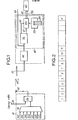
- the data dissemination system of fig. 1 comprises a transmitting station comprising transmission equipment 41 and a television broadcasting antenna 42, as well as a plurality of subscriber receiving stations comprising a reception antenna 43, a television receiver 44 and data reception equipment 45 .
- the transmission equipment 41 comprises a unit 46, called the manager, which is responsible for multiplexing the data messages over time from a plurality of data sources which, in the example described, is assumed to be limited to seven sources 247 to 253, sources which are capable of transmitting conventional data as well as data offering possibilities for error correction and encryption.
- the equipment 41 also comprises a modulation part 54 which receives, on the one hand, the signals transmitted by the manager and, on the other hand, video signals by a link 55, and which transmits signals to a conventional transmitter, not shown, which feeds the antenna 42.
- a modulation part 54 which is not part of the present invention, in the patent FR-A? 2313825 already cited, and in particular in relation to FIG. 4 of it.
- Fig. 2 shows an example of data packets transmitted by the manager 46, then, after modulation, by the antenna 42.
- the packet has a length of N bytes numbered 1 to N and consists of two parts.
- the first part called the prefix
- the number N always remains less than a number Nmax which can vary, depending on the standard of the television network which provides the broadcasting, and can be determined by optimization, taking into account the length of the useful television line and the bandwidth.
- Nmax can reach 40, which corresponds to the L standard recommended by the CCIR.
- bytes 1 and 2 are reserved for the synchronization of the bits of the packet and each consist of the sequence of bits 10101010.
- Byte 3, called the beginning conventionally allows synchronization byte by byte and can correspond to the sequence 11100111.
- Bytes 4, 5 and 6 are reserved for the identification of the digital channel, or source, and are developed in coded form by the manager 46.
- Byte 7, called continuity makes it possible to count packet numbers or indices from 1 to 15 and, therefore, to report packet omissions or errors in receiving equipment.
- byte 8 indicates the format of the packet, that is to say the number of M bytes which follow the prefix to form the packet.
- the television receiver 44 transmits, by its video output, the video signals to the equipment 45.
- the latter comprises a demodulation part 56, a logic part 124 and a reader 58 of an encoded medium 59.
- the demodulation part 56 delivers at 124 a bit frequency signal by 60 and the (N-3) x last 8 bits of the packet of N bytes by 61.
- the information read by the reader 58 is permanently applied to the logic part 124.
- the reception part 124 delivers at 62 the bytes of the packet data to an appropriate terminal, such as 63, plus a signal on a link 176 which will be described in FIG. 5.
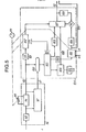
- Fig. 3 shows an omnibus line 65, a control circuit 66 and a coupler 267, capable of connecting any of the sources 247 to 253 to the line 65. Note that there are as many couplers as there are sources.
- line 65, circuit 66 and couplers 267 constitute the manager 46, fig. 1.
- the control circuit 66 is connected to 65 and can command the couplers 267 to connect to 65.
- the circuit 66 will not be described in detail, since it is identical to the circuit 76 in FIG. 3 of French patent FR-A No 2313825. It will simply be recalled that the circuit 66 sends, in the form of addresses, interrogations to the couplers in order to collect the identities of the couplers ready to transmit, then successively transmits transmission orders to these couplers.
- connection 68 connected to an address identification circuit 69 comprising the components 90, 92 and 126 of FIG. 3 of the French patent FR-A? 2313825.
- Circuit 69 has its output connected to the first input of an AND gate 111 whose output is connected to 65.
- junction 70 The data coming from the source associated with the coupler 267 are transmitted by a junction 70 of the type described in patent FR-A No 2268308.
- junction 70 the data enters, in parallel bytes, in an input logic circuit 71, the output of which is connected, on the one hand, to an input of an AND gate 268 and, on the other hand, to an input of an AND gate 279.
- the output of the AND gate 268 is connected to the input of an intermediate buffer 170 the output of which is connected to the input of an OR gate 280 the output of which is connected to the input of a buffer memory 72.
- the output of the AND gate 279 is connected at the other input of the OR gate 280.
- the source is connected to the coupler 267 by a wire 269 whose level 1 indicates that the source transmits layer 4 data, and whose level 0 indicates that it transmits conventional data.
- the forward service wire of the link 70 which transmits a change of state for each byte transmitted by 70, is connected to the input of a byte counter 73 whose output is connected, of a firstly, to an input of an AND gate 270 the output of which is connected to a register 74 which contains the number of bytes transmitted by 71 to the intermediate buffer memory 170 and, secondly, to an input of a AND gate 271, the output of which is connected to an input of an OR gate 272.
- the register 74 has a reset input (RESET) connected to line 65, an output connected to the first input of the AND gate 75, an output connected to the second input of the OR gate 272, and an output connected to the input of a memory counter 171.
- RESET reset input
- the counter 171 has a control input connected, by a link 172, to line 65, and its output is connected to an input of an AND gate 273, the output of which is connected to an input of an OR gate 274, the output of which is connected to memory 72 by the link 173.
- the buffer memory 72 comprises two parts, one 76 in which the bytes of the packet prefix are stored and the other 77 in which are stored bytes of data from the source by 71 and 170.
- the part 76 has a first entry linked to a memory 78 which contains the bytes 1 to 3 for synchronization and start, a second entry linked to a memory 79 which contains the three bytes 4 to 6 for identifying each packet prefix, a third entry linked to a packet counter 80 which delivers the packet number, that is to say the continuity byte, and a fourth input connected to the output of the OR gate 274 which delivers, at the time of transmission, either the number bytes contained in part 77, that is to say the content of counter 171, that is to say the value 0 contained in a memory 281 the output of which is connected to an input of an AND gate 282 the output of which is connected to the second entry of OR gate 274, i.e. the format byte which whatever its origin.
- the output of 81 is connected to an input of an OR gate 83, to an input of an AND gate 275 the output of which is connected to the first input of an AND gate 84, and to an input of an AND gate 276, the output of which is connected to a third input of the OR gate 89.
- the output of the OR gate 83 is connected to an inhibition input of the circuit 71.
- the coupler also includes a simulation circuit 85, which receives a speed indication coming from 66 by 65 and a link 86. This indication depends on the operating speed of the reception equipment capable of receiving the data from the source. With this speed information, the simulator 85 simulates dumps of the buffer memory 72, these dumps being counted in a counter 87 connected to the output of 85.
- the account outputs 1 to 4 of 87 are connected to the inputs of a OR gate 88 whose output is connected to the second input of the AND gate 84.
- the output 4 of 87 is connected to an input of an AND gate 277 whose output is connected to the second input of the AND gate 75.
- the outputs of AND gates 75 and 84 are respectively connected to the first two inputs of OR gate 89 of the output is connected to the second input of AND gate 111.
- the output of AND gate 75 is still connected to an input from OR gate 83.
- the output of memory 72 is connected to a transmit logic circuit 90 which receives from 65, via link 91, the bit frequency signal and, via link 92, the send order from the control circuit 66.
- the output of circuit 90 is connected to line 65 by wire 93 which transmits in series, bit by bit, the packet to the modulation part of the transmission equipment.
- the link 92 is also connected to the input of the counter 80 which, in this way, can count the packets sent by the coupler 267.
- circuit 171 has an output connected, via AND gate 273, OR gate 274 and link 173, to part 76 of 72. Its second output is connected to an input of an AND gate 278, the output of which is connected, by a link 174, to the read control input of the buffer memory 170.
- the memory 170 is a memory whose content is emptied in the part 77 of 72 at each order from 171.
- the wire 269, parallel to the link 70, is connected, on the one hand, to the second inputs of the AND gates 271, 276, 279 and, on the other hand, to the input of an inverter 283 whose output is connected to the second inputs of AND gates 268, 270, 273, 275, 277 and 278.
- the operator of the source associated with the coupler considered always transmits only significant data and that he does not have to be concerned with either the number Mmax or the frequency of transmission of the bits.
- the demodulation part of a subscriber reception equipment is shown in fig. 5.
- the signals leaving the television receiver 44 are applied to an impedance matching circuit 95, the output signal of which is applied, on the one hand, to a circuit 96 for recovering the bit frequency and, on the other hand, to a synchronization circuit 97.
- the synchronization circuit 97 comprises the circuits bearing the numerical references in FIG. 5 of patent FR-A No 2313825 and is used in particular to recognize the start byte so as to transmit to the logic part 124, by the link 61, only the fourth byte of each packet and the following ones.
- the circuit 96 comprises, like the conventional circuits for recovering the bit frequency, a tuned circuit comprising a variable impedance component 98, which can be a varicap, the impedance of which is controlled by the television channel selector 99.
- the circuit 96 delivers the bit frequency signal, on the one hand, to the synchronization circuit 97 and, on the other hand, to circuit 124 via the link 60.
- the signal at the frequency of the bits is applied, on the one hand, to a byte register 100 and, on the other hand, to a divider by eight 101 whose output is connected to the input d a byte counter 102.
- the bits of the packet are applied by 61 in series to the data input of the byte register 100 which transmits the bytes in parallel to a routing circuit 103.
- the byte counter 102 has its first six outputs corresponding to the first six bytes received in 124, that is to say bytes 4 to 9, connected to control input of the routing circuit 103, whose inputs activated successively have the effect of successively direct the bytes of the packet to the validation circuit 106 for bytes 4,5, 6 and 7, to a Hamming correction circuit 190 for byte 8, and to a data buffer 105 for the following bytes .
- the output of the correction circuit 190 is connected to the input of a transcoding circuit 125, the output of which is connected to the format register 104.
- the validation circuit 106 can include the circuits 168,179,166,171,167 shown in FIG. 6 of patent FR-A No 2313825 already cited and, optionally, circuits 173 and 174 of this same figure.
- the circuit validates the data received for their local use.
- the output of the buffer memory 105 is connected to the input of a switching circuit 107 which can be activated by a link 108 coming from 106.
- the output of 107 is connected to a junction 62, of the junction type 70 of fig. 3, which is connected to the user equipment 63.
- a wire from the junction 62 is connected to the input of a counter 109 counting the bytes transmitted by 107 and the output of which is connected to an input of a comparator 110, the other input of which is connected to the output of the format register 104 and the output of which is connected to an inhibition input of the circuit 107.
- the output of the byte counter 102 is connected to a validation input of circuit 107.
- the counter 102 activates its output when it reaches the Nmax count.
- the buffer memory 105 has received Nmax bytes of which possibly only P packet bytes are valid, P representing the total length of the packet.
- circuit 106 validates the packet
- the bytes can be transferred from 105 to 62 via 107.
- the inputs of comparator 110 have equal values and the output of 110 prohibits any other transmission from 105 to 62, for the television line considered which is used to support the packet.
- the Hamming correction circuit is a conventional circuit which will not be described, while the transcoding circuit 191 makes it possible, from bits b2, b4, b6 and b8 of the format byte, to find the real length of the block, which is transmitted to 104, or to determine that it is a layer 4 data packet.
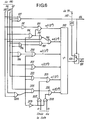
- the circuit 191 may be provided in the form indicated in FIG. 6.
- the output of the television channel selector 99 is also connected to a control input of the transcoding circuit 191 which includes not only an output to the register 104, but a second output 126 which follows a path parallel to the link 62.
- the input wires b2, b4, b6 and b8 transmit the four bits delivered by the correction circuit 190, in increasing order of the weights.
- the input wire b8 is connected, on the one hand, to the input of an inverter 192 whose output is connected to an input of a NOR gate 193 whose output delivers a signal of value 2 5 or 0 on the wire a5 and, on the other hand, to an input of a NAND gate 195 whose output is connected to an input of a NAND gate 198 whose output delivers a signal value 2 4 or 0 on wire a4.
- the input wire b6 is retained, on the one hand, at an input of a NOR gate 194 whose output is connected to the second input of the NAN D 195 gate and to the second input of the NOR gate 193 and, on the other hand, to an input of a NAND gate 197 whose output is connected to the second input of the NAN gate D 198.
- the input wire b4 is connected, on the one hand, to an input of a AND gate 196 whose output is connected to the second input of the NOR gate 194, to the second input of the NAND gate 197 and to the first input of a NOR gate with three inputs 200 and, on the other hand, to the first input of a NOR 199 gate, the output of which is connected to the second input of the NOR 200 gate, the output of which outputs a signal of value 2 3 or 0 on the wire a3.
- the input wire b2 is connected, on the one hand, to the second input of the NAN D 196 gate, on the other hand, to the second input of the NAN D 199 gate and, finally, to the first input of a NOR 201 gate which delivers a signal of value 2 2 or 0 on wire a2.
- the input wire b4 is also connected to an input of an AND gate 202 whose output is connected to an input of an OR gate 203 which delivers a signal of value 2 1 or 0 on the wire a1.
- the input wire b2 is also connected to the first input of an AND gate 205, the output of which is connected to an input of an OR gate 206 which delivers a signal with a value of 2 ° or 0 on the wire a0.
- Wire b6 is also connected to an input of a NOR gate 204 whose output is connected, in parallel, to the third input of the NOR gate 200, to the second input of the NOR gate 201, to the second input of the AND gate 202, at the second input of the AND gate 205 and at the input of an inverter 209.
- the output of the inverter 209 is connected to the first inputs of two AND gates 207 and 208.
- the output of the gate 207 is connected to the second input of the OR gate 203, and the output of the gate 208 is connected to the second input of the OR gate 206.
- the second inputs of the AND gates 207 and 208 are respectively connected to two control wires a and b.
- the input wires b2, b4, b6 and b8 are also connected to the four inputs of an OR gate 127, the output of which is connected to the control input of an electronic switch 128, the first signal input of which is connected to the output of the adder 210 and the output of which is connected to the register 104.
- the second signal input of the switch 128 is connected to the output of a memory 129 in which a predetermined number is stored, which is preferably the maximum number Nmax of bytes.
- the link 130 between 99 and 129 makes it possible to vary the number Nmax as a function of the television channel selected.
- the output of the OR gate 127 is still connected to the link 126.
- the output of the OR gate 127 When the format byte has a non-zero value, the output of the OR gate 127 is at 1, which switches the output of the adder 210 to the register 104; the operation is that which is described in patent EP-A No. 0026708 already cited. When the format byte has a zero value, the output of the OR gate 127 is at 0, which switches the output of the memory 129 to the register 104 which therefore stores the number Nmax. Furthermore, by the link 126, the output of the OR gate 127 indicates in parallel with the link 62 that the packet is not a conventional packet.
Landscapes
- Engineering & Computer Science (AREA)
- Signal Processing (AREA)
- Multimedia (AREA)
- Computer Hardware Design (AREA)
- Computer Networks & Wireless Communication (AREA)
- Computer Security & Cryptography (AREA)
- Data Exchanges In Wide-Area Networks (AREA)
- Time-Division Multiplex Systems (AREA)
Claims (3)
Applications Claiming Priority (2)
| Application Number | Priority Date | Filing Date | Title |
|---|---|---|---|
| FR8110089A FR2506100A2 (fr) | 1975-06-06 | 1981-05-14 | Systeme de diffusion de donnees |
| FR8110089 | 1981-05-14 |
Publications (2)
| Publication Number | Publication Date |
|---|---|
| EP0066487A1 EP0066487A1 (de) | 1982-12-08 |
| EP0066487B1 true EP0066487B1 (de) | 1984-10-24 |
Family
ID=9258699
Family Applications (1)
| Application Number | Title | Priority Date | Filing Date |
|---|---|---|---|
| EP82400832A Expired EP0066487B1 (de) | 1981-05-14 | 1982-05-05 | Datenübertragungssystem und in diesem System verwendete Sende- und Empfangsausrüstung |
Country Status (4)
| Country | Link |
|---|---|
| US (1) | US4496975A (de) |
| EP (1) | EP0066487B1 (de) |
| CA (1) | CA1198791A (de) |
| DE (1) | DE3261045D1 (de) |
Families Citing this family (12)
| Publication number | Priority date | Publication date | Assignee | Title |
|---|---|---|---|---|
| FR2514974B1 (fr) * | 1981-10-15 | 1986-11-28 | Telediffusion Fse | Systeme de diffusion de donnees par paquets |
| US4965825A (en) | 1981-11-03 | 1990-10-23 | The Personalized Mass Media Corporation | Signal processing apparatus and methods |
| US7831204B1 (en) | 1981-11-03 | 2010-11-09 | Personalized Media Communications, Llc | Signal processing apparatus and methods |
| USRE47642E1 (en) | 1981-11-03 | 2019-10-08 | Personalized Media Communications LLC | Signal processing apparatus and methods |
| DE3440796C2 (de) * | 1984-11-08 | 1986-10-16 | Schröter, Klaus, 1000 Berlin | Kommunikationssystem |
| US4956709A (en) * | 1988-03-11 | 1990-09-11 | Pbs Enterprises, Inc. | Forward error correction of data transmitted via television signals |
| SE462360B (sv) * | 1988-10-28 | 1990-06-11 | Ellemtel Utvecklings Ab | Foerfarande och anordning foer att foerhindra att det paa en gemensam oeverfoeringslaenk saends datapaket med hoegre intensitet aen ettfoerutbestaemt vaerdesitet aen ett foerutbestaemt vaerde |
| JP3262142B2 (ja) * | 1992-01-16 | 2002-03-04 | 富士通株式会社 | Atmセル化装置、atmセル化方法、ノード、及びノードにおける多重化方法 |
| FR2716550B1 (fr) * | 1994-02-24 | 1996-05-15 | Bertin & Cie | Mémoire de masse chiffrante du type embarquable et procédé de protection des informations enregistrées dans cette mémoire. |
| US5953418A (en) * | 1995-06-14 | 1999-09-14 | David Hall | Providing selective data broadcast receiver addressability |
| WO1997000564A2 (en) * | 1995-06-15 | 1997-01-03 | Hall, David | Communication system for superimposing data onto a video signal |
| US20150264599A1 (en) * | 2014-03-12 | 2015-09-17 | Cinet Inc. | Non-intrusive method of sending the transmission configuration information from the transmitter to the receiver |
Family Cites Families (3)
| Publication number | Priority date | Publication date | Assignee | Title |
|---|---|---|---|---|
| FR2313825A1 (fr) * | 1975-06-06 | 1976-12-31 | Telediffusion Fse | Systeme de diffusion de donnees |
| FR2393480A2 (fr) * | 1977-06-03 | 1978-12-29 | Telediffusion Fse | Systeme de diffusion de donnees |
| FR2466917A2 (fr) * | 1979-09-27 | 1981-04-10 | Telediffusion Fse | Systeme de diffusion de donnees |
-
1982
- 1982-05-05 DE DE8282400832T patent/DE3261045D1/de not_active Expired
- 1982-05-05 EP EP82400832A patent/EP0066487B1/de not_active Expired
- 1982-05-10 US US06/376,790 patent/US4496975A/en not_active Expired - Fee Related
- 1982-05-11 CA CA000402718A patent/CA1198791A/en not_active Expired
Also Published As
| Publication number | Publication date |
|---|---|
| US4496975A (en) | 1985-01-29 |
| CA1198791A (en) | 1985-12-31 |
| EP0066487A1 (de) | 1982-12-08 |
| DE3261045D1 (en) | 1984-11-29 |
Similar Documents
| Publication | Publication Date | Title |
|---|---|---|
| EP0026708B1 (de) | System zum Senden von Daten und Empfangsausrüstung für ein solches System | |
| EP0066487B1 (de) | Datenübertragungssystem und in diesem System verwendete Sende- und Empfangsausrüstung | |
| EP0152341B1 (de) | Verfahren zur Fernsteuerung von elektrischen Geräten und entsprechender Empfänger | |
| EP0014653B1 (de) | System zur Informationsübertragung zwischen einer Zentrale und Empfangsstationen, welches System mit Mitteln zum Steuern des Zugangs zur übertragenen Information ausgerüstet ist | |
| CA1150429A (fr) | Installation de commutation numerique a division du temps pour des lignes vehiculant la parole et des paquets de donnees | |
| FR2525420A1 (fr) | Systeme de transmission de donnees sur un reseau de cables | |
| FR2505114A1 (fr) | Systeme de traitement de donnees video de television | |
| WO1998003026A1 (fr) | Message court ameliore et procede de synchronisation et de securisation d'un echange de messages courts ameliores dans un systeme de radiocommunication cellulaire | |
| FR2669798A1 (fr) | Dispositif pour la transmission d'informations synchrones par un reseau asynchrone, notamment un reseau atm. | |
| EP0078185B1 (de) | Rundfunk-Datenpakete-Empfänger | |
| FR2495872A1 (fr) | Ensemble et procede de traitement de donnees video de television | |
| WO1991007849A1 (fr) | Procede d'embrouillage et de desembrouillage de signaux video composites, et dispositif de mise en ×uvre | |
| EP0601653A1 (de) | System zur Übertragung von Information mit unterschiedlichen Bitraten und Sendestation für ein solches System | |
| WO1980002630A1 (fr) | Systeme de videotex muni de moyens de protection contre les erreurs de transmission | |
| FR2558321A1 (fr) | Dispositif programmable de filtrage deterministe de messages | |
| FR2642245A1 (fr) | Systeme de reception et de traitement de trames hdlc transmises sur liaison mic multivoies a multiplexage temporel, notamment pour commutateur de donnees | |
| EP0648063B1 (de) | Methode und Anlage für die Transmission von Sätzen von ATM-Zellen | |
| EP0389339B1 (de) | Interaktives Verteilnetz für Video-, Ton- und Computermitteilungsnachrichten | |
| EP0639012A1 (de) | Verfahren und Vorrichtung zum Überwachen und/oder Testen eines ATM-Telekommunikationsnetzes | |
| EP0097579A1 (de) | Funkverbindungssystem nach dem Frequenzsprungverfahren mit Redundanz zwischen den einzelnen Frequenzstufen | |
| FR2933564A1 (fr) | Procede d'embrouillage et desembrouillage pour le transport de flux de donnees audio video mpeg2 | |
| FR2818859A1 (fr) | Procede et dispositif de filtrage des donnees relatives au guide electronique de programmes d'un televiseur | |
| FR2506100A2 (fr) | Systeme de diffusion de donnees | |
| FR2496376A1 (fr) | Procede et systeme de teletexte pour l'affichage de donnees sur l'ecran d'un recepteur de television | |
| EP0660990A1 (de) | Verfahren und system zur steuerung der art des zugangs zu signalen, insbesondere bildsignalen |
Legal Events
| Date | Code | Title | Description |
|---|---|---|---|
| PUAI | Public reference made under article 153(3) epc to a published international application that has entered the european phase |
Free format text: ORIGINAL CODE: 0009012 |
|
| AK | Designated contracting states |
Designated state(s): BE DE GB NL |
|
| 17P | Request for examination filed |
Effective date: 19830516 |
|
| GRAA | (expected) grant |
Free format text: ORIGINAL CODE: 0009210 |
|
| AK | Designated contracting states |
Designated state(s): BE DE GB NL |
|
| REF | Corresponds to: |
Ref document number: 3261045 Country of ref document: DE Date of ref document: 19841129 |
|
| PLBE | No opposition filed within time limit |
Free format text: ORIGINAL CODE: 0009261 |
|
| STAA | Information on the status of an ep patent application or granted ep patent |
Free format text: STATUS: NO OPPOSITION FILED WITHIN TIME LIMIT |
|
| 26N | No opposition filed | ||
| PGFP | Annual fee paid to national office [announced via postgrant information from national office to epo] |
Ref country code: GB Payment date: 19920406 Year of fee payment: 11 |
|
| PGFP | Annual fee paid to national office [announced via postgrant information from national office to epo] |
Ref country code: NL Payment date: 19920531 Year of fee payment: 11 |
|
| PGFP | Annual fee paid to national office [announced via postgrant information from national office to epo] |
Ref country code: BE Payment date: 19920626 Year of fee payment: 11 |
|
| PGFP | Annual fee paid to national office [announced via postgrant information from national office to epo] |
Ref country code: DE Payment date: 19920725 Year of fee payment: 11 |
|
| PG25 | Lapsed in a contracting state [announced via postgrant information from national office to epo] |
Ref country code: GB Effective date: 19930505 |
|
| PG25 | Lapsed in a contracting state [announced via postgrant information from national office to epo] |
Ref country code: BE Effective date: 19930531 |
|
| BERE | Be: lapsed |
Owner name: L' ETAT FRANCAIS REPRESENTE PAR LE MINISTRE DES P. Effective date: 19930531 Owner name: TELEDIFFUSION DE FRANCE Effective date: 19930531 |
|
| PG25 | Lapsed in a contracting state [announced via postgrant information from national office to epo] |
Ref country code: NL Effective date: 19931201 |
|
| GBPC | Gb: european patent ceased through non-payment of renewal fee |
Effective date: 19930505 |
|
| NLV4 | Nl: lapsed or anulled due to non-payment of the annual fee | ||
| PG25 | Lapsed in a contracting state [announced via postgrant information from national office to epo] |
Ref country code: DE Effective date: 19940201 |