EP0066729A1 - Verfahren zum Prüfen der Funktion einer programmierbaren logischen Anordnung - Google Patents
Verfahren zum Prüfen der Funktion einer programmierbaren logischen Anordnung Download PDFInfo
- Publication number
- EP0066729A1 EP0066729A1 EP82104236A EP82104236A EP0066729A1 EP 0066729 A1 EP0066729 A1 EP 0066729A1 EP 82104236 A EP82104236 A EP 82104236A EP 82104236 A EP82104236 A EP 82104236A EP 0066729 A1 EP0066729 A1 EP 0066729A1
- Authority
- EP
- European Patent Office
- Prior art keywords
- output lines
- output
- lines
- array
- row
- Prior art date
- Legal status (The legal status is an assumption and is not a legal conclusion. Google has not performed a legal analysis and makes no representation as to the accuracy of the status listed.)
- Granted
Links
- 238000010998 test method Methods 0.000 title claims description 5
- 238000012360 testing method Methods 0.000 claims abstract description 76
- 238000012217 deletion Methods 0.000 claims abstract description 40
- 230000037430 deletion Effects 0.000 claims abstract description 40
- 239000011159 matrix material Substances 0.000 claims abstract description 8
- 238000000034 method Methods 0.000 claims description 16
- 238000003466 welding Methods 0.000 claims description 16
- 238000012544 monitoring process Methods 0.000 claims description 11
- 230000004044 response Effects 0.000 claims description 10
- 230000002950 deficient Effects 0.000 abstract description 21
- 238000009877 rendering Methods 0.000 abstract description 3
- 230000006870 function Effects 0.000 description 16
- 238000003491 array Methods 0.000 description 13
- 238000005516 engineering process Methods 0.000 description 7
- 230000002093 peripheral effect Effects 0.000 description 6
- PCTMTFRHKVHKIS-BMFZQQSSSA-N (1s,3r,4e,6e,8e,10e,12e,14e,16e,18s,19r,20r,21s,25r,27r,30r,31r,33s,35r,37s,38r)-3-[(2r,3s,4s,5s,6r)-4-amino-3,5-dihydroxy-6-methyloxan-2-yl]oxy-19,25,27,30,31,33,35,37-octahydroxy-18,20,21-trimethyl-23-oxo-22,39-dioxabicyclo[33.3.1]nonatriaconta-4,6,8,10 Chemical compound C1C=C2C[C@@H](OS(O)(=O)=O)CC[C@]2(C)[C@@H]2[C@@H]1[C@@H]1CC[C@H]([C@H](C)CCCC(C)C)[C@@]1(C)CC2.O[C@H]1[C@@H](N)[C@H](O)[C@@H](C)O[C@H]1O[C@H]1/C=C/C=C/C=C/C=C/C=C/C=C/C=C/[C@H](C)[C@@H](O)[C@@H](C)[C@H](C)OC(=O)C[C@H](O)C[C@H](O)CC[C@@H](O)[C@H](O)C[C@H](O)C[C@](O)(C[C@H](O)[C@H]2C(O)=O)O[C@H]2C1 PCTMTFRHKVHKIS-BMFZQQSSSA-N 0.000 description 5
- 230000004913 activation Effects 0.000 description 4
- 238000010420 art technique Methods 0.000 description 3
- 238000005192 partition Methods 0.000 description 3
- 150000001875 compounds Chemical class 0.000 description 2
- 239000004020 conductor Substances 0.000 description 2
- 230000007547 defect Effects 0.000 description 2
- 230000000694 effects Effects 0.000 description 2
- 238000006467 substitution reaction Methods 0.000 description 2
- 230000003213 activating effect Effects 0.000 description 1
- 230000004888 barrier function Effects 0.000 description 1
- 230000008901 benefit Effects 0.000 description 1
- 230000000295 complement effect Effects 0.000 description 1
- 238000010276 construction Methods 0.000 description 1
- 230000009849 deactivation Effects 0.000 description 1
- 230000001419 dependent effect Effects 0.000 description 1
- 238000013461 design Methods 0.000 description 1
- 230000005669 field effect Effects 0.000 description 1
- 230000002452 interceptive effect Effects 0.000 description 1
- 238000003698 laser cutting Methods 0.000 description 1
- 230000008018 melting Effects 0.000 description 1
- 238000002844 melting Methods 0.000 description 1
- 238000012986 modification Methods 0.000 description 1
- 230000004048 modification Effects 0.000 description 1
- 229920000747 poly(lactic acid) Polymers 0.000 description 1
- 230000008569 process Effects 0.000 description 1
- 238000007711 solidification Methods 0.000 description 1
- 230000008023 solidification Effects 0.000 description 1
- 238000000638 solvent extraction Methods 0.000 description 1
- 238000012956 testing procedure Methods 0.000 description 1
Images

Classifications
-
- G—PHYSICS
- G01—MEASURING; TESTING
- G01R—MEASURING ELECTRIC VARIABLES; MEASURING MAGNETIC VARIABLES
- G01R31/00—Arrangements for testing electric properties; Arrangements for locating electric faults; Arrangements for electrical testing characterised by what is being tested not provided for elsewhere
- G01R31/28—Testing of electronic circuits, e.g. by signal tracer
- G01R31/317—Testing of digital circuits
- G01R31/3181—Functional testing
- G01R31/3185—Reconfiguring for testing, e.g. LSSD, partitioning
- G01R31/318516—Test of programmable logic devices [PLDs]
-
- H—ELECTRICITY
- H03—ELECTRONIC CIRCUITRY
- H03K—PULSE TECHNIQUE
- H03K19/00—Logic circuits, i.e. having at least two inputs acting on one output; Inverting circuits
- H03K19/02—Logic circuits, i.e. having at least two inputs acting on one output; Inverting circuits using specified components
- H03K19/173—Logic circuits, i.e. having at least two inputs acting on one output; Inverting circuits using specified components using elementary logic circuits as components
- H03K19/177—Logic circuits, i.e. having at least two inputs acting on one output; Inverting circuits using specified components using elementary logic circuits as components arranged in matrix form
- H03K19/17704—Logic circuits, i.e. having at least two inputs acting on one output; Inverting circuits using specified components using elementary logic circuits as components arranged in matrix form the logic functions being realised by the interconnection of rows and columns
-
- H—ELECTRICITY
- H03—ELECTRONIC CIRCUITRY
- H03K—PULSE TECHNIQUE
- H03K19/00—Logic circuits, i.e. having at least two inputs acting on one output; Inverting circuits
- H03K19/02—Logic circuits, i.e. having at least two inputs acting on one output; Inverting circuits using specified components
- H03K19/173—Logic circuits, i.e. having at least two inputs acting on one output; Inverting circuits using specified components using elementary logic circuits as components
- H03K19/177—Logic circuits, i.e. having at least two inputs acting on one output; Inverting circuits using specified components using elementary logic circuits as components arranged in matrix form
- H03K19/17736—Structural details of routing resources
-
- H—ELECTRICITY
- H03—ELECTRONIC CIRCUITRY
- H03K—PULSE TECHNIQUE
- H03K19/00—Logic circuits, i.e. having at least two inputs acting on one output; Inverting circuits
- H03K19/02—Logic circuits, i.e. having at least two inputs acting on one output; Inverting circuits using specified components
- H03K19/173—Logic circuits, i.e. having at least two inputs acting on one output; Inverting circuits using specified components using elementary logic circuits as components
- H03K19/177—Logic circuits, i.e. having at least two inputs acting on one output; Inverting circuits using specified components using elementary logic circuits as components arranged in matrix form
- H03K19/17736—Structural details of routing resources
- H03K19/17744—Structural details of routing resources for input/output signals
-
- H—ELECTRICITY
- H03—ELECTRONIC CIRCUITRY
- H03K—PULSE TECHNIQUE
- H03K19/00—Logic circuits, i.e. having at least two inputs acting on one output; Inverting circuits
- H03K19/02—Logic circuits, i.e. having at least two inputs acting on one output; Inverting circuits using specified components
- H03K19/173—Logic circuits, i.e. having at least two inputs acting on one output; Inverting circuits using specified components using elementary logic circuits as components
- H03K19/177—Logic circuits, i.e. having at least two inputs acting on one output; Inverting circuits using specified components using elementary logic circuits as components arranged in matrix form
- H03K19/17748—Structural details of configuration resources
- H03K19/17764—Structural details of configuration resources for reliability
Definitions
- This invention generally relates to arrays or matrices (PLAs) which are used for performing logic functions, and more particularly to a logic array which includes provisions for fully testing the array logic function.
- PLAs arrays or matrices
- Logic arrays are presently used by digital circuit designers as alternatives to custom wired logic gate chains for implementing a given logic function.
- Logic arrays generally include a first plurality of input lines for accepting digital input signals, and a second plurality of orthogonally oriented output lines for providing digital output signals.
- a logical element is located at at least some of the intersections of input and output lines to form an array or matrix of logical elements.
- the logic array is not personalized, i.e., the logical elements are not connected.
- the logical elements are personalized, i.e., selected logical elements are connected to their adjacent input and output lines. By connecting the proper logical elements, any desired logic function may be implemented. Techniques have been developed in the art for determining which logical elements should be personalized in order to implement a given logic function. Techniques have also been developed in the art to minimize the size of the array necessary to implement a given logic function.
- Logic arrays are presently available employing various types of logical element technologies, e.g., Schottky barrier diodes, transistors, or FETs.
- Personalization takes place by either breaking a conductor connecting a logical element with an adjacent input or output line, or by melting adjacent conductors so that they weld to form a conducting path therebetween upon solidification to connect a logical element with an input or output line.
- the personalization technique depends generally upon the array technology. In either case, the breaking or welding may be accomplished through the use of a miniaturized laser.
- Logic arrays are currently available in many sizes and in various array configurations, i.e., two or more arrays may be incorporated on a single chip in order to readily implement standardized logic functions.
- One currently available compound logic array configuration is the Programmable Logic Array (PLA) comprising a plurality of input and output columns and a plurality of rows orthogonal to the input and output columns.
- PPA Programmable Logic Array
- An "AND” or “product” array of logical elements is located at the intersections of the input columns and the rows, while an “OR” or “sum” array of logical elements is located at the intersections of the output columns and the rows.
- the prior art technique for testing array personalization is inadequate in that it may not spot all possible personalization defects. This is so because in a logic array there is not a one-to-one correspondence between digital input patterns and array output lines activated. In other words, a given digital input pattern may activate more than one output line. An output from the logic array in response to a given input bit pattern may show that an array output line has been activated, but not necessarily the correct array output line. Thus, it is sometimes impossible to detect defective personalization even if many combinations of input patterns are applied.
- the array personalization includes many "don't cares". Due to the presence of "don't cares" in the array personalization, a given input pattern will generally activate more than one PLA row. If the output columns are monitored for a given logical output in response to a given digital input, it cannot be ascertained whether this logical output is due to the activation of the proper row or is due to another row being activated by the given digital input. Due to the nature of the associative match in the PLA, it may be impossible to detect the defective personalization of a given row.
- the object is achieved by a logic array and a method of testing said logic array as defined in the characterizing part of claim 1 and claim 10 respectively.
- a logic array the individual output lines of which may be disabled so that the disabled line will not provide an output despite the activation thereof by an appropriate input signal.
- a disabling means may be provided by the addition of a deletion control line and means for selectively connecting the deletion control line to one or more of the array output lines. When the deletion control line is connected to an array output line, the connected output line is disabled.
- personalization of a given output line may be tested without interference from the remainder of the array output lines.
- the entire array may be personalized and tested in a line by line fashion, as follows: The logical elements associated with the first output line are personalized. An input pattern which activates the first output line is then applied to the input lines, and the proper response to the input pattern is verified. The first output line is then connected to the deletion control line to disable the first output line for the remainder of the personalization and test operations. The second output line may then be tested as above without interference from the first output line.
- the above personalizing and testing sequence is repeated for each output line until the entire array has been personalized and tested. After each output line is tested it is disabled to prevent interference with subsequent tests. Once the array has been fully personalized and tested, the deletion control line is deactivated thereby enabling all output lines for proper array operation.
- the testing of an entire array may be accomplished using only one input word per output line, greatly minimizing array test time. Further, since each output line is disabled after it is tested, interference with subsequent testing is precluded, to insure 100% testing of personalization.
- deletion control line When the deletion control line is incorporated into a logic array in accordance with the present invention, a further advantage results. Since personalization and testing is done on a line by line basis, it is immediately known when a given output line's personalization is defective. A defective array may be rendered usable by permanently deactivating the defective output line and personalizing another output line to the personalization pattern desired. By providing spare or extra output lines, substitution of spare lines for defective lines may take place, thereby rendering a defective array usable.
- PLA 10 programmable logic array
- PLA 10 consists of two arrays; a first array 11 is generally referred to as an "AND” or “product” array and a second array 12 generally referred to as an "OR” or “sum” array.
- the output lines of the AND array are also the input lines for the OR array and will be referred to as PLA rows 17.
- Input lines 16 of the AND array will be referred to as input columns, the output lines 18 of the OR array will be referred to as output columns.
- PLA 10 also includes additional peripheral circuitry.
- Input latches 21 are employed for storing digital input signals from inputs 23.
- Output latches 22 are employed for storing the PLA output to be provided on output lines 24.
- the array also may include a partition circuit or decoder 19. Partition circuits may be employed to minimize the number of input columns 16 by generating complementary logical functions of the input signals as will be described below with regard to Fig. 2.
- Logical elements 13 may be bipolar transistors, field effect transistors, diodes or other elements.
- each logical element 13 is disconnected from either its adjacent row or column so that an open circuit is present.
- each logical element 13 is connected to an adjacent column 16 or 18 but is not connected to its adjacent row 17. Provision is made, however, for connecting a logical element 13 to its adjacent row 17 by application of laser energy to laser welding sites 14.
- PLA 10 further includes a test line 26 orthogonal to PLA rows 17, and a connecting element 27 at the intersection of each row 17 and test line 26. Provision is made for connecting connection elements 26 to its adjacent row 17 by application of laser energy to laser welding sites 14.
- Test line 26 is employed for monitoring the logical state of rows 17 which are connected to test line 26 by elements 27 in a "wired OR" configuration. If any of the PLA rows 17 are in their active logical state, test line 26 will also be active. Conversely, in order for test line 26 to be inactive, all rows 17 must be inactive. It will be understaood by those having skill in the art that the terms “active” corresponds to logic high or low depending upon the particular PLA configuration state. Likewise the term “inactive” corresponds to the logic state which is not active, and may be logic high or low dependingupon the particular PLA configuration.
- a given input signal will generally activate more than one row. Even if the row under test 17c is defective, and is not activated, one of the other rows 17 may be activated, and will test line 26. This will give the impression that the personalization of row 17c is proper when in fact it may not be proper.
- deletion control line 28 is an added column orthogonal to PLA rows 17.
- Deleting elements 29 are added between the deletion control line 28 and each row 17 of PLA 10.
- deletion elements 29 are of the same technology as logical elements 13.
- Deletion control line 28 provides the capability of disabling a row 17 after it has been tested so that it will not interfere with testing of subsequent rows.
- deletion control line 28 is connected at 30 to a suitable voltage source.
- the voltage level of the voltage source is such that when a deleting element 29 is connected to a row 17, the row 17 will be clamped at a logic level which precludes activation of test line 26, i.e., the row will be held at its inactive logic level.
- the voltage level at 30 will depend upon the PLA technology, and may in fact be zero volts or ground potential.
- the testing of the PLA of Fig. 1 in accordance with the present invention will now be described: Initially the PLA is in its unpersonalized state. Personalization and testing proceeds one row at a time.
- the logical elements of the first row 17a of AND array 11 are personalized according to a predetermined personalization pattern by laser welding.
- the connecting element 27 between test line 26 and row 17a is laser welded.
- the digital input bit pattern which activates the first row of AND array 11 is then applied to PLA input lines 23. If test line 26 is activated, this indicates that the personalization is accurate.
- the logical elements of the first row 17a of OR array 12 are then personalized according to a predetermined personalization pattern by laser welding.
- OR array personalization (first row) is then tested by applying the same digital input bit pattern which was applied above, and by observing PLA output lines 24 for proper output. Personalization and testing of row 17a are now complete.
- row 17a is disabled by laser welding the topmost deleting element 29 to row 17a. This maintains row 17a in its low inactive state regardless of the digital input presented on lines 23 and, row 17a cannot activate test line 26 during subsequent row testing.
- the personalization and testing procedure described above is then repeated for each subsequent row, on a row-by-row basis, until all of the rows have been individually personalized and tested.
- Deletion control line 28 is then deactivated by connecting point 30 to a suitable voltage source (which may be zero volts) such that the connection of deleting elements 29 to rows 17 has no effect on the output of rows 17. This effectively deactivates the deletion control line, and all of the array rows may be employed to generate the PLA logical function.
- a suitable voltage source which may be zero volts
- the PLA of Fig. 1 include.s spare rows 17e and 17f. If, in testing rows 17a...17d, one row, for example, 17b, is found to be defective, a spare row, such as 17e, may replace row 17b by personalizing spare row 17e with the proper personalization originally intended for defective row 17b. Spare row 17e is tested in accordance with the present invention in the same manner as a regular row. Defective row 17b may be permanently deleted, for instance, by laser personalizing the defective row to an unused input pattern, thus assuring that it will never be activated by a given input. It will be noted that defective row substitution may only be accomplished in a PLA incorporating the present invention, as otherwise it is impossible to determine when a given PLA row is defective.
- test line 26 and connecting element 27 may be dispensed with, and the OR array itself used for testing the personalization of AND array 11 on a row-by-row basis. This may be accomplished by personalizing both the AND and OR arrays of a given row at the same time. A digital input pattern which activates the personalized row is then applied to PLA input lines 23. PLA output lines 24 are tested for the proper response. If the response is proper then personalization of the given row (for both AND and OR arrays) is proper. The given row is then disabled by connecting its deleting element 29 to deletion control line 28, and testing may proceed on the remainder of the PLA rows.
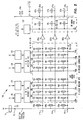
- Fig. 2 a specific example of a small scale PLA is illustrated in Fig. 2. It will be recognized by those having skill in the art that the PLA of Fig. 2 contains all the elements of a commercially available PLA, albeit in reduced numbers for the sake of simplicity of description.
- a small scale PLA 100 using bipolar technology and logic levels of +V volts and 0 volts for logic high (1) and logic low (0), respectively, is illustrated.
- the PLA architecture includes inverters 125a-125c between the outputs 117a-117c of AND array 111 and the inputs 120a-120c of OR array 112.
- Test line 126 includes a plurality of connecting elements 127a-127c.
- Deletion control line 128 includes a plurality of deleting elements 129a-129c.
- connecting elements 127, deleting elements 129 and logical elements 150-176 are all bipolar NPN transistors.
- the collectors of all the NPN transistors are connected to V volts, however this connection is not shown in Fig. 2 for the sake of clarity.
- open laser welding sites are shown by open circles while laser welded connections are shown by blackened circles. Initially, all laser welding sites on the PLA are open.
- the PLA of Fig. 2 further includes four input latches 121 and an output latch 122.
- the PLA is of the bit partition type, i.e., logical inputs A, B, C and D are passed through a pair of 2 to 4 decoders 119, to generate the four logical functions of two input variable pairs, i.e., AB, AB, AB, and AB.
- Bit partitioning of a PLA is well known to those having skill in the art and will not be further described here.
- the PLA of Fig. 2 includes a deletion control line 128 and deleting elements 129a-129c in accordance with the present invention. Prior to personalization, deletion control line 128 is connected to +V volts (logic high).
- Row 117a is personalized according to a predetermined pattern; i.e., transistors 153, 164 and 165 are laser welded to form the logical function AB + CD + CD.
- Connecting element 127a is laser welded.
- the operability of the transistors connecting row 117a and the proper personalization thereof is then tested by applying an input to input lines A, B, C and D which will activate row 117a.
- row l17a will be activated, corresponding in this example to logic low. Conversely, if personalization is improper, row 117a will be high. As a result of the presence of inverter 125a, corresponding OR array row 120a will be high for proper personalization and low for improper personalization. Thus, proper personalization is verified by test line 126 being high upon application of an input pattern which activates row 117a. It will be noted further that since transistors 127b and 127c have not yet been laser welded, interference by unpersonalized rows 120b and 120c with the output of test line 126 is precluded, regardless of the logical state of rows 120b and 120c.
- the process proceeds by personalizing the first row 120a of OR array 112 by laser welding transistor 174.
- transistor 129a is laser welded to connect deletion control line 128 with row 117a. Since the deletion control line is connected to +V, row 117a will always be at logic high thus rendering row 120a at logic low thus ensuring that transistor 127a is always off. Test line 126 therefore is never activated by row 120a.
- row 117b may commence in a manner analogous with row 117a.
- Row 117b is personalized according to a predetermined pattern, i.e., transistors 167 and 169 are laser welded to form a logical function C D + CD.
- transistors 154-157 are also laser welded, for purposes which are described below in connection with the permanent deactivation of row 117b).
- the PLA includes spare row 117c.
- spare row 117c may be substituted for defective row 117b.
- Defective row 117b may be permanently rendered inactive by laser welding all four outputs of a 2 to 4 decoder 119 in the defective row 117b.
- transistors 154-157 are all laser welded. By welding all four outputs of a 2 to 4 decoder 119, it is assured that no matter what logical values A or B takes on, one of the transistors 154-157 will always be on thus driving row 117b to its logic high state and driving row 120b to its logic low state. Row 120b therefore can never contribute to the output of the PLA for any possible input bit pattern. Row 117b is thus effectively removed from the PLA.
- row 120c of OR array 112 may be personalized by laser welding transistor 176 to column 116i.
- the proper laser personalization may be verified by observing the output of column 116i in output latch 122, as was described with respect to row 120a above. Again, it will be noted that the only way output column 116i may be activated is via transistor 176, since transistor 174 in row 120a has been disabled by the deletion control line.
- test line 126 The proper personalization of each row of OR array 112 was tested by monitoring the output of the OR array itself. It will be understood by those having skill in the art, however, that test line 126 may be eliminated and the personalization of the AND array verified by monitoring the output of the OR array. This may be accomplished by personalizing both the AND and OR array for a given row before testing the personalization of the row, as was described with regard to Fig. 1.
- connecting elements 127 may be permanently connected to test line 126, if the PLA design incorporates means for maintaining unpersonalized AND array rows 117 at logic high, thus precluding interference by an unpersonalized row with the activation of test line 126.
- deletion control line 128 is deactivated by removing the deletion control line from the +V volt source and grounding the deletion control line. This may be accomplished by laser cutting the deletion control line at point 131 and laser welding the deletion control line to ground by laser welding at 132. Since deletion control line 128 is now grounded, transistors 129 are off and rows 117a-117c may be activated in accordance with the PLA input bit pattern. Deletion control line 128 is effectively removed from the circuit.
- the present invention may be employed in logic arrays of various configurations and sizes. Further, the invention is not technology dependent as it may be readily adapted to logic arrays employing FET, Schottky or other technology. It is also well known to those having skill in the art that a single chip may employ a folded array structure wherein two PLA's are incorporated thereon in a mirror image configuration. In such a case, each PLA may incorporate a separate deletion control line, as each PLA in the folded array is essentially independent.
Landscapes
- Physics & Mathematics (AREA)
- Mathematical Physics (AREA)
- Engineering & Computer Science (AREA)
- General Engineering & Computer Science (AREA)
- Computer Hardware Design (AREA)
- Computing Systems (AREA)
- Computer Networks & Wireless Communication (AREA)
- General Physics & Mathematics (AREA)
- Logic Circuits (AREA)
- Design And Manufacture Of Integrated Circuits (AREA)
- Test And Diagnosis Of Digital Computers (AREA)
Applications Claiming Priority (2)
| Application Number | Priority Date | Filing Date | Title |
|---|---|---|---|
| US06/270,435 US4435805A (en) | 1981-06-04 | 1981-06-04 | Testing of logic arrays |
| US270435 | 1994-07-05 |
Publications (2)
| Publication Number | Publication Date |
|---|---|
| EP0066729A1 true EP0066729A1 (de) | 1982-12-15 |
| EP0066729B1 EP0066729B1 (de) | 1985-11-21 |
Family
ID=23031319
Family Applications (1)
| Application Number | Title | Priority Date | Filing Date |
|---|---|---|---|
| EP82104236A Expired EP0066729B1 (de) | 1981-06-04 | 1982-05-14 | Verfahren zum Prüfen der Funktion einer programmierbaren logischen Anordnung |
Country Status (4)
| Country | Link |
|---|---|
| US (1) | US4435805A (de) |
| EP (1) | EP0066729B1 (de) |
| JP (1) | JPS57203137A (de) |
| DE (1) | DE3267540D1 (de) |
Cited By (4)
| Publication number | Priority date | Publication date | Assignee | Title |
|---|---|---|---|---|
| EP0126322A1 (de) * | 1983-05-06 | 1984-11-28 | International Business Machines Corporation | Prüfbare logische Anordnung |
| FR2566210A1 (fr) * | 1984-06-18 | 1985-12-20 | Monolithic Memories Inc | Reseau logique programmable comportant des circuits de test et de verification |
| GB2211310A (en) * | 1987-10-20 | 1989-06-28 | Gazelle Microcircuits Inc | Programmable multiplexer circuit |
| GB2252694A (en) * | 1990-11-09 | 1992-08-12 | Dataproducts Corp | Printer having a multiple scan line printhead controller |
Families Citing this family (19)
| Publication number | Priority date | Publication date | Assignee | Title |
|---|---|---|---|---|
| DE3135368A1 (de) * | 1981-09-07 | 1983-03-31 | Siemens AG, 1000 Berlin und 8000 München | Verfahren und anordnung zur funktionspruefung einer programmierbare logikanordnung |
| DE3220302C2 (de) * | 1982-05-28 | 1984-03-15 | Siemens AG, 1000 Berlin und 8000 München | Programmierbare Logikanordnung in ECL-Technik |
| US4503387A (en) * | 1982-12-30 | 1985-03-05 | Harris Corporation | A.C. Testing of logic arrays |
| US4499579A (en) * | 1983-03-10 | 1985-02-12 | Honeywell Information Systems Inc. | Programmable logic array with dynamic test capability in the unprogrammed state |
| US4542508A (en) * | 1983-11-21 | 1985-09-17 | Aerojet-General Corporation | Amenable logic gate and method of testing |
| WO1986003592A1 (en) * | 1984-12-11 | 1986-06-19 | Aerojet-General Corporation | Amenable logic gate and method of testing |
| US4749947A (en) * | 1986-03-10 | 1988-06-07 | Cross-Check Systems, Inc. | Grid-based, "cross-check" test structure for testing integrated circuits |
| US5365165A (en) * | 1986-09-19 | 1994-11-15 | Actel Corporation | Testability architecture and techniques for programmable interconnect architecture |
| US5309091A (en) * | 1986-09-19 | 1994-05-03 | Actel Corporation | Testability architecture and techniques for programmable interconnect architecture |
| US5083083A (en) * | 1986-09-19 | 1992-01-21 | Actel Corporation | Testability architecture and techniques for programmable interconnect architecture |
| US5341092A (en) * | 1986-09-19 | 1994-08-23 | Actel Corporation | Testability architecture and techniques for programmable interconnect architecture |
| US5367208A (en) * | 1986-09-19 | 1994-11-22 | Actel Corporation | Reconfigurable programmable interconnect architecture |
| US4862069A (en) * | 1987-08-05 | 1989-08-29 | Genrad, Inc. | Method of in-circuit testing |
| US5065090A (en) * | 1988-07-13 | 1991-11-12 | Cross-Check Technology, Inc. | Method for testing integrated circuits having a grid-based, "cross-check" te |
| US5528600A (en) * | 1991-01-28 | 1996-06-18 | Actel Corporation | Testability circuits for logic arrays |
| US5347519A (en) * | 1991-12-03 | 1994-09-13 | Crosspoint Solutions Inc. | Preprogramming testing in a field programmable gate array |
| JP2930013B2 (ja) * | 1996-06-27 | 1999-08-03 | 日本電気株式会社 | Pla・dac回路 |
| WO2007015479A1 (ja) * | 2005-08-01 | 2007-02-08 | Matsushita Electric Industrial Co., Ltd. | プログラマブル・ロジック・アレイ及びプログラマブル・ロジック・アレイモジュールジェネレータ |
| US8868820B2 (en) * | 2011-10-31 | 2014-10-21 | Microsemi SoC Corporation | RAM block designed for efficient ganging |
Citations (1)
| Publication number | Priority date | Publication date | Assignee | Title |
|---|---|---|---|---|
| US3987286A (en) * | 1974-12-20 | 1976-10-19 | International Business Machines Corporation | Time split array logic element and method of operation |
Family Cites Families (14)
| Publication number | Priority date | Publication date | Assignee | Title |
|---|---|---|---|---|
| NL267533A (de) | 1960-07-29 | |||
| US4025902A (en) | 1972-07-31 | 1977-05-24 | Toyoda Koki Kabushiki Kaisha | General purpose sequence controller |
| US3803562A (en) | 1972-11-21 | 1974-04-09 | Honeywell Inf Systems | Semiconductor mass memory |
| US3958110A (en) | 1974-12-18 | 1976-05-18 | Ibm Corporation | Logic array with testing circuitry |
| US4032894A (en) | 1976-06-01 | 1977-06-28 | International Business Machines Corporation | Logic array with enhanced flexibility |
| US4124899A (en) | 1977-05-23 | 1978-11-07 | Monolithic Memories, Inc. | Programmable array logic circuit |
| US4217658A (en) | 1977-07-25 | 1980-08-12 | Struthers-Dunn, Inc. | Process control system that controls its outputs according to the results of successive analysis of the vertical input columns of a hypothetical ladder diagram |
| US4227247A (en) | 1977-10-12 | 1980-10-07 | Eaton Corporation | Integrated circuit controller programmable with unidirectional-logic instructions representative of sequential wire nodes and circuit elements of a ladder diagram |
| JPS5483340A (en) * | 1977-12-15 | 1979-07-03 | Nec Corp | Logic array |
| JPS5483341A (en) * | 1977-12-15 | 1979-07-03 | Nec Corp | Digital integrated circuit |
| US4249246A (en) | 1978-02-27 | 1981-02-03 | Nippon Electric Co., Ltd. | Programmable logic array for generating EOR sums of input signals |
| US4234956A (en) | 1978-10-11 | 1980-11-18 | The General Electric Company Limited | Digital relay systems |
| US4244034A (en) | 1979-01-09 | 1981-01-06 | Westinghouse Electric Corp. | Programmable dual stack relay ladder line solver and programming panel therefor |
| US4354228A (en) | 1979-12-20 | 1982-10-12 | International Business Machines Corporation | Flexible processor on a single semiconductor substrate using a plurality of arrays |
-
1981
- 1981-06-04 US US06/270,435 patent/US4435805A/en not_active Expired - Lifetime
-
1982
- 1982-04-09 JP JP57058343A patent/JPS57203137A/ja active Granted
- 1982-05-14 EP EP82104236A patent/EP0066729B1/de not_active Expired
- 1982-05-14 DE DE8282104236T patent/DE3267540D1/de not_active Expired
Patent Citations (1)
| Publication number | Priority date | Publication date | Assignee | Title |
|---|---|---|---|---|
| US3987286A (en) * | 1974-12-20 | 1976-10-19 | International Business Machines Corporation | Time split array logic element and method of operation |
Non-Patent Citations (3)
| Title |
|---|
| IBM TECHNICAL DISCLOSURE BULLETIN, Vol. 20, No. 1, June 1977, New York, E.I. MUEHLDORF et al. "PLA Macro Optimized Test Pattern Generation" pages 47 to 53 * |
| IBM TECHNICAL DISCLOSURE BULLETIN, Vol. 22, No. 5, October 1979, New York, W.W. WU "Pretesting Laserable PLA Peripheral Circuits" pages 1868 to 1869 * |
| IBM TECHNICAL DISCLOSURE BULLETIN, Vol. 24, No. 1A, June 1981, New York, W.M. CHU et al. "PLA with Product Term Test Circuit" page 131 * |
Cited By (8)
| Publication number | Priority date | Publication date | Assignee | Title |
|---|---|---|---|---|
| EP0126322A1 (de) * | 1983-05-06 | 1984-11-28 | International Business Machines Corporation | Prüfbare logische Anordnung |
| FR2566210A1 (fr) * | 1984-06-18 | 1985-12-20 | Monolithic Memories Inc | Reseau logique programmable comportant des circuits de test et de verification |
| GB2161608A (en) * | 1984-06-18 | 1986-01-15 | Monolithic Memories Inc | Programmable array logic circuit with testing and verification circuitry |
| GB2161608B (en) * | 1984-06-18 | 1989-07-19 | Monolithic Memories Inc | Programmable array logic circuit with testing and verification circuitry |
| GB2211310A (en) * | 1987-10-20 | 1989-06-28 | Gazelle Microcircuits Inc | Programmable multiplexer circuit |
| US4897836A (en) * | 1987-10-20 | 1990-01-30 | Gazelle Microcircuits, Inc. | Programmable connection path circuit |
| GB2252694A (en) * | 1990-11-09 | 1992-08-12 | Dataproducts Corp | Printer having a multiple scan line printhead controller |
| US5347617A (en) * | 1990-11-09 | 1994-09-13 | Dataproducts Corporation | Printer having a multiple scan line printhead controller |
Also Published As
| Publication number | Publication date |
|---|---|
| US4435805A (en) | 1984-03-06 |
| JPH0218497B2 (de) | 1990-04-25 |
| EP0066729B1 (de) | 1985-11-21 |
| DE3267540D1 (en) | 1986-01-02 |
| JPS57203137A (en) | 1982-12-13 |
Similar Documents
| Publication | Publication Date | Title |
|---|---|---|
| US4435805A (en) | Testing of logic arrays | |
| EP0076124B1 (de) | Verfahren zum Prüfen von IC-Speichern | |
| KR910003147B1 (ko) | 반도체집적회로와 그 시험방법 | |
| US7216277B1 (en) | Self-repairing redundancy for memory blocks in programmable logic devices | |
| US3958110A (en) | Logic array with testing circuitry | |
| WO1981002360A1 (en) | Block redundancy for memory array | |
| US6021512A (en) | Data processing system having memory sub-array redundancy and method therefor | |
| JPH0658936B2 (ja) | ラッチ支援ヒューズテスト回路及びラッチ支援ヒューズテスト方法 | |
| KR950015694A (ko) | 번-인회로를 가지는 반도체 메모리장치 및 그 번-인방법 | |
| US6397349B2 (en) | Built-in self-test and self-repair methods and devices for computer memories comprising a reconfiguration memory device | |
| US5982683A (en) | Enhanced method of testing semiconductor devices having nonvolatile elements | |
| EP0126322B1 (de) | Prüfbare logische Anordnung | |
| US5805514A (en) | Method for testing a semiconductor memory device and a semiconductor memory device | |
| JP2988380B2 (ja) | 半導体試験装置およびこの試験装置を用いた試験方法 | |
| US6288958B1 (en) | Semiconductor storage device and burn-in test method | |
| EP0760518B1 (de) | Vorrichtung und Verfahren zur Prüfung von Einzelbitfehlern in integrierten Speicherschaltungen | |
| US6601194B1 (en) | Circuit configuration for repairing a semiconductor memory | |
| JPH06295594A (ja) | 半導体記憶装置 | |
| US11880607B2 (en) | Memory with fuse pins shared by multiple-type repairs | |
| US6697291B2 (en) | Method for checking a conductive connection between contact points | |
| US4410987A (en) | Preload test circuit for programmable logic arrays | |
| US6345013B1 (en) | Latched row or column select enable driver | |
| US5841787A (en) | Memory programming and test circuitry and methods for implementing the same | |
| KR100196513B1 (ko) | 프리 리페어회로 | |
| KR100631911B1 (ko) | 반도체 메모리 장치에서의 리던던시 메모리 셀 테스트 방법 |
Legal Events
| Date | Code | Title | Description |
|---|---|---|---|
| PUAI | Public reference made under article 153(3) epc to a published international application that has entered the european phase |
Free format text: ORIGINAL CODE: 0009012 |
|
| AK | Designated contracting states |
Designated state(s): DE FR GB |
|
| 17P | Request for examination filed |
Effective date: 19830420 |
|
| GRAA | (expected) grant |
Free format text: ORIGINAL CODE: 0009210 |
|
| AK | Designated contracting states |
Designated state(s): DE FR GB |
|
| REF | Corresponds to: |
Ref document number: 3267540 Country of ref document: DE Date of ref document: 19860102 |
|
| ET | Fr: translation filed | ||
| PLBE | No opposition filed within time limit |
Free format text: ORIGINAL CODE: 0009261 |
|
| STAA | Information on the status of an ep patent application or granted ep patent |
Free format text: STATUS: NO OPPOSITION FILED WITHIN TIME LIMIT |
|
| 26N | No opposition filed | ||
| PGFP | Annual fee paid to national office [announced via postgrant information from national office to epo] |
Ref country code: GB Payment date: 19920409 Year of fee payment: 11 |
|
| PGFP | Annual fee paid to national office [announced via postgrant information from national office to epo] |
Ref country code: FR Payment date: 19920427 Year of fee payment: 11 |
|
| PGFP | Annual fee paid to national office [announced via postgrant information from national office to epo] |
Ref country code: DE Payment date: 19920523 Year of fee payment: 11 |
|
| PG25 | Lapsed in a contracting state [announced via postgrant information from national office to epo] |
Ref country code: GB Effective date: 19930514 |
|
| GBPC | Gb: european patent ceased through non-payment of renewal fee |
Effective date: 19930514 |
|
| PG25 | Lapsed in a contracting state [announced via postgrant information from national office to epo] |
Ref country code: FR Effective date: 19940131 |
|
| PG25 | Lapsed in a contracting state [announced via postgrant information from national office to epo] |
Ref country code: DE Effective date: 19940201 |
|
| REG | Reference to a national code |
Ref country code: FR Ref legal event code: ST |