EP0067083B1 - Schaltungsanordnung zur Korrektur von Farbsignalen aus einer Fernsehkamera zur Verbesserung der Bildwahrnehmung - Google Patents
Schaltungsanordnung zur Korrektur von Farbsignalen aus einer Fernsehkamera zur Verbesserung der Bildwahrnehmung Download PDFInfo
- Publication number
- EP0067083B1 EP0067083B1 EP82400821A EP82400821A EP0067083B1 EP 0067083 B1 EP0067083 B1 EP 0067083B1 EP 82400821 A EP82400821 A EP 82400821A EP 82400821 A EP82400821 A EP 82400821A EP 0067083 B1 EP0067083 B1 EP 0067083B1
- Authority
- EP
- European Patent Office
- Prior art keywords
- values
- input
- output
- circuit
- value
- Prior art date
- Legal status (The legal status is an assumption and is not a legal conclusion. Google has not performed a legal analysis and makes no representation as to the accuracy of the status listed.)
- Expired
Links
- 238000012937 correction Methods 0.000 title claims description 38
- 230000008447 perception Effects 0.000 title claims description 7
- 230000006870 function Effects 0.000 claims description 22
- 238000012546 transfer Methods 0.000 claims description 10
- 230000001186 cumulative effect Effects 0.000 claims description 9
- 238000005315 distribution function Methods 0.000 claims description 8
- 239000003086 colorant Substances 0.000 claims description 2
- 238000004364 calculation method Methods 0.000 description 7
- 235000021183 entrée Nutrition 0.000 description 4
- 238000000034 method Methods 0.000 description 4
- 230000005540 biological transmission Effects 0.000 description 2
- 230000003247 decreasing effect Effects 0.000 description 2
- 241001080024 Telles Species 0.000 description 1
- 238000010586 diagram Methods 0.000 description 1
- 238000012986 modification Methods 0.000 description 1
- 230000004048 modification Effects 0.000 description 1
- 238000012545 processing Methods 0.000 description 1
- 238000005070 sampling Methods 0.000 description 1
Images

Classifications
-
- H—ELECTRICITY
- H04—ELECTRIC COMMUNICATION TECHNIQUE
- H04N—PICTORIAL COMMUNICATION, e.g. TELEVISION
- H04N9/00—Details of colour television systems
- H04N9/77—Circuits for processing the brightness signal and the chrominance signal relative to each other, e.g. adjusting the phase of the brightness signal relative to the colour signal, correcting differential gain or differential phase
-
- H—ELECTRICITY
- H04—ELECTRIC COMMUNICATION TECHNIQUE
- H04N—PICTORIAL COMMUNICATION, e.g. TELEVISION
- H04N23/00—Cameras or camera modules comprising electronic image sensors; Control thereof
- H04N23/10—Cameras or camera modules comprising electronic image sensors; Control thereof for generating image signals from different wavelengths
- H04N23/13—Cameras or camera modules comprising electronic image sensors; Control thereof for generating image signals from different wavelengths with multiple sensors
Definitions
- the present invention relates to devices for correcting color information supplied by a camera of a video transmission system with a view to obtaining, on reception, an image containing the maximum of visible information.
- a correction device In black and white image transmission systems, a correction device is already known in order to improve the perception of images (European patent application n ° 19518 filed by the Applicant).
- the method implemented by this device consists in correcting the luminance signal supplied by the analyzer tube of a black and white camera using a nonlinear quadrupole with variable characteristics, controlled in such a way that the histogram of the values of the corrected luminance signal, has a flat shape whatever the shooting conditions, which corresponds to a regular distribution of the values on the scale of these values.
- this correction device does not make it possible to improve color images. It only improves the black and white images.
- the present invention relates to a correction device for improving the perception of color images.
- the problem consists in correcting the overall luminance according to the method implemented by the known device while retaining the original chromaticity of the image analyzed.
- the device receives the three color pieces of information, of value V e1 , V e2 , V e3 , consisting respectively of the three signals of blue, green, red color, of values E B , E v , E R , applied respectively to three input terminals 1, 2 and 3. It provides three corrected color information, with values: V s1 , V s2 , V s3 , on three output terminals, 15, 16, 17.
- the value of the overall luminance is:
- the correction of the overall luminance consists in multiplying this value by a variable coefficient G:
- the value Ey being a linear combination of E v , E R , E B , to preserve the chromaticity it suffices to multiply by the same coefficient G the three values E V , E R , E B.
- the coefficient G varies when Ey varies, because it is determined so as to flatten the histogram of the values V e of a signal which is constituted, in this exemplary embodiment, by the global luminance signal.
- the correction device provides three color signals having the corrected value:
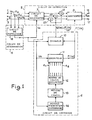
- FIG. 1 represents a block diagram of the first embodiment of the device according to the invention, which implements this method.
- three input terminals 1, 2 and 3 are shown, intended respectively to receive the three color signals V e1 , V e2 and V e3 supplied by the analyzer tubes of a color camera. These three input terminals are respectively coupled to the three inputs of a circuit 4 for determining a signal V e , constituted by a matrixing circuit 4. The output of this matrixing circuit 4 delivers the signal V e , which is consisting, in this example, of the global luminance signal.
- V e 0.11 ⁇ V e1 + 0.59 ⁇ V e2 + 0.3 ⁇ V e3 ⁇ (V e1 , V e2 and V e3 ) corresponding respectively to the blue, green and red color signals).
- the output of the matrixing circuit 4 is connected to an input of a control circuit 6.
- the control circuit 6 comprises means 14 for acquiring a histogram, an analog quadrupole 11 and an analog divider 10, each having a input connected to the circuit input command 6, and it further comprises calculation means 13 and auxiliary calculation means 12.
- the quadrupole 11 is non-linear and has variable characteristics adjustable by eight control inputs e 1 to e 8 intended to receive eight signals defining the quadrupole transfer parameters.
- This quadrupole 11 is of known type having a broken line transfer function consisting of a predetermined number of linear segments. In the example described, the quadrupole 11 was chosen with eight variable transfer parameters, that is to say four couples, consisting of a threshold value and a gain value, defining four segments.
- Such a quadrupole comprises four amplifiers (not shown), having an adjustable threshold below which no signal is transmitted and above which the signals are transmitted with a fixed gain.
- the quadrupole 11 delivers a corrected luminance signal F (V e ), F being the transfer function of the quadrupole.
- This signal F (V e ) corresponds to the sum of the four output signals of the four amplifiers of the quadrupole, it is supplied to a second input of the divider 10 and to a second output of the control circuit 6.
- the means 14 statistically analyze the amplitude distribution of 4,000 samples of the luminance signal V e , according to 64 given amplitude levels.
- the 4,000 samples result from the analysis of 4,000 domains covering an entire frame, and the 64 amplitude levels are distributed at regular intervals over the entire amplitude scale of the luminance.
- the means 14 therefore make it possible to acquire the representative function of the histogram of the luminance (number of samples for each of the 64 levels envisaged).
- the calculation means 13 calculate the integral of this function, this integral being, by definition, the cumulative distribution function of the amplitude levels of the samples.
- the auxiliary calculation means 12 having an input connected to the output of the means 13 and eight outputs respectively connected to the eight control inputs e 1 to e 8 of the quadrupole 11, calculate the values of the eight transfer parameters A 1 to A 4 and G 1 to G 4 to be applied to the control inputs e 1 to e e , A i to G i (i varying from 1 to 4) representing respectively the threshold values and the gain values quadrupole amplifiers.
- the calculated values are such that the transfer function F carried out by the quadrupole 11 is an approximation by segments of the cumulative distribution function calculated by the means 13.
- the parameter values thus determined remain fixed for the duration of the following frame.
- Such a transfer function transforms the luminance signal V e into a corrected signal F (V e ) for which the distribution of the values allows better vision whatever the shooting conditions.
- the distribution corresponds to an equalization of the histogram of the luminance associated with the signal F (V e ).
- the assembly constituted by the quadrupole 11, the means 14 for acquiring a histogram, the calculation means 13 and the auxiliary calculation means 12, corresponds exactly to the automatic control device described in detail in the patent application cited in beginning of this text.
- the aim of the invention is to correct the color information V e1 , V e2 and V e3 so that the overall luminance information, associated with the corrected color information, corresponds to the luminance information contained in the signal F (V e ) while retaining the original chromaticity of the analyzed image.
- the three input terminals 1, 2 and 3 are respectively connected to the first three inputs of a correction circuit 5 of which a second input, a third and a fourth inputs are connected respectively to the first output of the control circuit 6, at the output of the determination circuit 4, and at the second output of the control circuit 6.
- the correction circuit 5 is constituted, in this embodiment, by a subtraction circuit 7 having the first three inputs constituting the three first inputs of the correction circuit 5, by three analog multipliers 21, 22, 23 having three first inputs connected respectively to three outputs of the subtraction circuit 7, having three second inputs connected together to constitute the second input of the correction circuit 5, and having three outputs connected respectively to three inputs of an adder 9.
- the subtraction circuit 7 has a second input constituting the third input of the correction circuit.
- the adder 9 has a second input constituting the fourth input of the correction circuit 5 and three outputs constituting respectively three outputs of the correction circuit 5, which are connected to the three output terminals 15, 16, 17 of the device according to the invention.
- the subtraction circuit 7 has three outputs providing respectively three color difference signals DV e1 , DV e2 and DV e3 . These three signals are developed from the signals V el , V e2 , V e3 and V e according to the following formulas:
- the multipliers 21, 22, 23 respectively generate three signals DV s1 , DV s2 and DV s3 from the signals G (V e ), DV e1 , DV e2 and DV e3 according to the following formulas
- the three outputs of the adder 9 respectively supply three signals V s1 , V s2 and V s3 produced from the signals DV s1 , DV s2 , DV s3 and F (V e ) according to the following formulas:
- the correction circuit 5 transforms the color information V e1 , V e2 and V e3 associated with the global luminance signal V e into corrected color information V s1 , V s2 and V s3 associated with the corrected overall luminance signal F (V e ).
- V e the corrected overall luminance signal
- the quadrupole 11 may include any number of variable parameters in order to better adapt the transfer function to the cumulative distribution function; the same applies to the number of samples and the number of amplitude levels of the luminance signal.
- control device 6 or one of its elements can easily be produced using a microcomputer.
- V e It is also possible to directly generate the signal G (V e ) using a digital memory.
- the analog signal V e is then converted into digital values which are applied to the address inputs of a memory in which a microcomputer has previously stored the values of G (V e ).
- the output of the memory is then connected to the input of a digital-analog converter which delivers the signal G (V e ).
- the matrixing circuit 4 generates a signal V e which corresponds to the global luminance signal calculated with the conventional coefficients (0.11; 0.59; 0.3).
- the invention is applicable from a signal V e corresponding to a different combination of color information. For example, excellent results have been obtained by taking as signal V e the signal corresponding to max (V e1 ; V e2 ; V e3 ).
- the invention can easily be applied from the three color signals E Y , D R , D B , transmitted by color television. Indeed, the processing to be subjected to these three signals is deduced simply from that exposed for the three primary signals E B , E V and E R , these two triplets of signals being linked by linear relations.
- FIG. 2 represents a second embodiment of the device according to the invention.
- the determination circuit 4 supplies a signal with a value V e which is not equal to the overall luminance value, but which is equal to the largest of the values among those of the three signals of color, E R , E v , E B at the sampling instant considered:
- the correction consists in correcting the overall luminance while preserving the original chromaticity of the image when the value G (V e ) is high, but not when it is low.
- the corrected luminance value is greater than the original value, the device does not modify the saturation of the color.
- the corrected luminance value is lower than the original value, the perception of the image is improved by increasing the saturation of the color while maintaining the same hue.
- the signals of values V e1 , V e2 , V e3 consist of the global luminance signal of value Ey, and the color difference signals, of values D R and D B.
- the control circuit 6 develops the value G (V e ) by a digital process implemented by a microprocessor.
- a determination circuit 4 is constituted by a demosaicing circuit 25 having three inputs constituting three inputs of the determination circuit 4, and three outputs providing color signals of value E R , E V and E B , to three inputs of a selection circuit 26 which determines which of these values is the largest and routes this to an output constituting the output of the determination circuit 4.
- the value V e thus determined is applied to an input of the circuit of command 6.
- the control circuit 6 comprises an analog-digital converter 27 whose input constitutes the input of the control circuit 6 and which converts the value V e from the analog form to the digital form.
- the control circuit 6 comprises a digital-analog converter 28 whose output constitutes an output of the control circuit 6 and provides in analog form a signal with a value G (V e ).
- the control circuit 6 also comprises means 32 for acquiring a histogram, a digital integrator 31, a microprocessor 30, and a random access memory 29.
- the means 32 calculate for each frame of an image the histogram of 4 000 values V e supplied by the output of the analog-digital converter 27, and supply the values of this histogram to the digital integrator 31 which calculates the values of the function of the cumulative distribution of this histogram and supplies them to an input of the microprocessor 30.
- the microprocessor 30 has two outputs connected respectively to a write address input and to a data input from memory 29. It calculates a table of the values of the function G (V e ) and stores this table in the memory 29.
- a first stage consists in determining a function F such that the histogram of the values of the corrected signal F (V e ) has a predetermined distribution over the whole of its scale of val eurs. For example, to have a regular distribution it suffices that the function F (V Q ) is equal to the cumulative distribution function of the values V e .
- the microprocessor 30 calculates 64 values of G (V e ), each of these values being chosen from 256 possible values, coded on eight bits. These values are stored in memory 29 which comprises 256 bytes.
- This memory includes a read address input connected to the output of the analog-digital converter 27, and a data output connected to the input of the digital-analog converter 28.
- the output of the determination 4 provides a value V e which is transmitted in digital form to the reading address input of the memory 29, the latter provides on its data output a digital value G (V e ) which is converted into the form analog by the digital-analog converter 28, and which is applied to the output of the control circuit 6.
- the correction circuit 5 comprises three analog multipliers 21, 22 and 23 having three first inputs and three outputs, constituting respectively three first inputs and three outputs of the correction circuit 5, and having three second inputs.
- the second input of the multiplier 21 is connected to a second input of the correction circuit 5 and the second inputs of the multipliers 22 and 23 are connected together to the output of a weighting circuit 24 having an input connected to a second input of the correction 5.
- the weighting circuit 24 is an analog circuit supplying at its output a signal of value H (V e ) equal to 1 when G (V e ) is less than or equal to 1, and a signal of value H (V e ) equal to G (V e ) when G (V e ) is greater than 1.
- the value G (V e ) is transmitted without modification when it is high, so the chromaticity is preserved when the correction consists in increasing the luminance of a shade , and on the other hand the saturation of the color is increased when the luminance of a hue is decreased.
- weighting circuit 24 It is within the reach of those skilled in the art to produce a weighting circuit 24 operating differently, it is in particular possible to use a weighting circuit providing a value such as: H (V e ): 1/2 ⁇ G (V e ) + 1/2.
- V e Max (E R , E v , E B ) avoids an exaggerated correction of the luminance signal when one of the values of the color signals is much higher than the other two.
Landscapes
- Engineering & Computer Science (AREA)
- Multimedia (AREA)
- Signal Processing (AREA)
- Processing Of Color Television Signals (AREA)
- Color Television Image Signal Generators (AREA)
Claims (7)
Applications Claiming Priority (2)
| Application Number | Priority Date | Filing Date | Title |
|---|---|---|---|
| FR8110253 | 1981-05-22 | ||
| FR8110253A FR2506549A1 (fr) | 1981-05-22 | 1981-05-22 | Dispositif de correction des informations couleur fournies par les tubes analyseurs d'une camera en vue d'ameliorer la perception des images |
Publications (2)
| Publication Number | Publication Date |
|---|---|
| EP0067083A1 EP0067083A1 (de) | 1982-12-15 |
| EP0067083B1 true EP0067083B1 (de) | 1984-06-13 |
Family
ID=9258804
Family Applications (1)
| Application Number | Title | Priority Date | Filing Date |
|---|---|---|---|
| EP82400821A Expired EP0067083B1 (de) | 1981-05-22 | 1982-05-04 | Schaltungsanordnung zur Korrektur von Farbsignalen aus einer Fernsehkamera zur Verbesserung der Bildwahrnehmung |
Country Status (6)
| Country | Link |
|---|---|
| US (1) | US4499486A (de) |
| EP (1) | EP0067083B1 (de) |
| JP (1) | JPS57197988A (de) |
| CA (1) | CA1197608A (de) |
| DE (1) | DE3260247D1 (de) |
| FR (1) | FR2506549A1 (de) |
Families Citing this family (20)
| Publication number | Priority date | Publication date | Assignee | Title |
|---|---|---|---|---|
| EP0138074B1 (de) * | 1983-09-16 | 1989-12-13 | Hitachi, Ltd. | Signalverarbeitungsschaltung für eine Farbvideokamera |
| JPS60151786A (ja) * | 1984-01-19 | 1985-08-09 | Fuji Photo Film Co Ltd | 放射線画像情報読取階調処理方法および装置 |
| FR2575884B1 (fr) * | 1985-01-08 | 1988-07-08 | Thomson Video Equip | Dispositif pour reduire la dynamique de trois signaux de couleur representant une image |
| US4764971A (en) * | 1985-11-25 | 1988-08-16 | Eastman Kodak Company | Image processing method including image segmentation |
| JPH0669438B2 (ja) * | 1987-04-24 | 1994-09-07 | 株式会社東芝 | 内視鏡装置 |
| JPS6354144A (ja) * | 1986-08-25 | 1988-03-08 | 株式会社東芝 | 電子内視鏡装置 |
| DE3629396C2 (de) * | 1986-08-29 | 1993-12-23 | Agfa Gevaert Ag | Verfahren zur elektronischen Bildverarbeitung |
| DE3629403C2 (de) * | 1986-08-29 | 1994-09-29 | Agfa Gevaert Ag | Verfahren zur Korrektur der Farbsättigung bei der elektronischen Bildverarbeitung |
| JP2522296B2 (ja) * | 1987-03-31 | 1996-08-07 | ソニー株式会社 | 映像信号の階調制御回路 |
| US4868651A (en) * | 1988-05-17 | 1989-09-19 | S&S Inficon, Inc. | Digital radiography with image brightness and contrast normalization |
| JP2582140B2 (ja) * | 1988-10-31 | 1997-02-19 | 株式会社日立製作所 | 投写形ディスプレイ |
| CA2040672C (en) * | 1990-04-26 | 1995-05-30 | Masaaki Kanashiki | Image signal processing apparatus |
| US5137364A (en) * | 1991-01-31 | 1992-08-11 | Mccarthy Cornelius J | Optical spectral analysis apparatus |
| BE1007590A3 (nl) * | 1993-10-01 | 1995-08-16 | Philips Electronics Nv | Videosignaalverwerkingsschakeling. |
| JP3134660B2 (ja) * | 1994-04-14 | 2001-02-13 | 松下電器産業株式会社 | 色変換方法および色変換装置 |
| JP3408316B2 (ja) * | 1994-04-18 | 2003-05-19 | 日本フィリップス株式会社 | ニー回路 |
| BR9804773B1 (pt) * | 1997-03-06 | 2010-12-14 | Panasonic Corporation | aparelho de compensaÇço do gama. |
| JP4257036B2 (ja) * | 1999-02-05 | 2009-04-22 | コーニンクレッカ フィリップス エレクトロニクス エヌ ヴィ | ヒストグラム等化方法 |
| EP1404116A1 (de) * | 2002-09-25 | 2004-03-31 | Dialog Semiconductor GmbH | Verfahren einer schnellen Farbsättigungskorrektur |
| JP2008242733A (ja) * | 2007-03-27 | 2008-10-09 | Seiko Epson Corp | 画像処理装置 |
Family Cites Families (9)
| Publication number | Priority date | Publication date | Assignee | Title |
|---|---|---|---|---|
| DE2018149C3 (de) * | 1970-04-16 | 1975-08-28 | Robert Bosch Gmbh, 7000 Stuttgart | Verfahren zur Erhöhung der Schärfe von Farbfernsehbildern und Schaltungsanordnung zur Durchführung des Verfahrens |
| US3684825A (en) * | 1971-02-19 | 1972-08-15 | Rca Corp | Contrast compression circuits |
| US3979555A (en) * | 1975-05-27 | 1976-09-07 | Hughes Aircraft Company | Histogram equalization system for display improvement |
| US3983320A (en) * | 1975-08-25 | 1976-09-28 | Hughes Aircraft Company | Raster display histogram equalization |
| GB2046051B (en) * | 1979-03-29 | 1983-01-26 | Philips Electronic Associated | Real time histogram modification system for image processing |
| FR2456448A1 (fr) * | 1979-05-11 | 1980-12-05 | Thomson Csf | Dispositif de commande automatique de la fonction de transfert d'un systeme de transmission videofrequence en vue d'ameliorer la perception des images |
| IL58119A (en) * | 1979-08-27 | 1983-03-31 | Yeda Res & Dev | Histogram image enhancement system |
| US4315319A (en) * | 1980-02-01 | 1982-02-09 | Rockwell International Corporation | Non-linear signal processor |
| US4394744A (en) * | 1981-02-12 | 1983-07-19 | The United States Of America As Represented By The Secretary Of The Navy | Real-time amplitude histogram shaper |
-
1981
- 1981-05-22 FR FR8110253A patent/FR2506549A1/fr active Granted
-
1982
- 1982-05-04 DE DE8282400821T patent/DE3260247D1/de not_active Expired
- 1982-05-04 EP EP82400821A patent/EP0067083B1/de not_active Expired
- 1982-05-18 CA CA000403228A patent/CA1197608A/en not_active Expired
- 1982-05-19 US US06/379,945 patent/US4499486A/en not_active Expired - Fee Related
- 1982-05-21 JP JP57087176A patent/JPS57197988A/ja active Pending
Also Published As
| Publication number | Publication date |
|---|---|
| JPS57197988A (en) | 1982-12-04 |
| US4499486A (en) | 1985-02-12 |
| CA1197608A (en) | 1985-12-03 |
| FR2506549A1 (fr) | 1982-11-26 |
| FR2506549B1 (de) | 1983-10-07 |
| EP0067083A1 (de) | 1982-12-15 |
| DE3260247D1 (en) | 1984-07-19 |
Similar Documents
| Publication | Publication Date | Title |
|---|---|---|
| EP0067083B1 (de) | Schaltungsanordnung zur Korrektur von Farbsignalen aus einer Fernsehkamera zur Verbesserung der Bildwahrnehmung | |
| JP3070860B2 (ja) | 画像データの増強方法およびカラー画像データの増強方法 | |
| Mann et al. | Beingundigital’with digital cameras | |
| EP0192497B1 (de) | Einrichtung zum Reduzieren der Dynamik der drei Farbbildsignale | |
| US9386288B2 (en) | Compensating for sensor saturation and microlens modulation during light-field image processing | |
| EP0298978B1 (de) | Verfahren zur digitalen farbbildverarbeitung mittels histogrammnormalisierung für ton- und farbreproduktion | |
| US5319472A (en) | Multispectral color image pickup system | |
| CA1229911A (en) | Apparatus and method for producing a still image video signal using solid-state imaging device | |
| EP0114559B1 (de) | Verfahren zur ständigen Farbkorrektur für Video-Bildaufnahme und System zur Durchführung des Verfahrens | |
| EP0019518B1 (de) | Vorrichtung zur automatischen Steuerung der Übertragungsfunktion eines Videofrequenzübertragungssystems um die Bildwahrnehmung zu verbessern | |
| EP0419342A1 (de) | Vorrichtung zur Fehlerkorrektur einer durch einen integrierten Matrix-Infrarotsensor abgetasteten Bilderfolge | |
| EP1396816A2 (de) | Bildschärfeverbesserung von numerischen Bildern | |
| WO2020233931A1 (fr) | Dispositif de capture d'images à expositions multiples et système de surveillance d'un conducteur associé | |
| EP1286553B1 (de) | Verfahren und Gerät zur Verbesserung der Bildqualität in digitalen Kameras | |
| EP4020978A1 (de) | Verfahren zur eichung einer matrix von photodetektoren, entsprechende eichungsvorrichtung und entsprechendes bildgebungssystem | |
| FR2510855A1 (fr) | Circuit d'echantillonnage et de maintien pour un circuit de separation de couleur | |
| CA1226654A (fr) | Dispositif de discrimination d'echos radar | |
| EP0609117A1 (de) | Gammakamera mit Verstärkungskompensation | |
| US5349546A (en) | Method and apparatus for non-linear signal processing with reduced upper harmonic components | |
| FR2563069A1 (fr) | Dispositif de traitement lineaire parcellaire de signaux video numeriques | |
| EP0085600A1 (de) | Einrichtung zur Entzerrung der durch einen Hochfrequenzsignalverstärker mit Spitzenwertregelung erzeugten Intermodulation | |
| EP0843867B1 (de) | Verfahren zur verarbeitung einer numerischen verrauschten quellbildsequenz | |
| EP3579186A1 (de) | Verfahren und system zur verwaltung einer landwirtschaftlichen parzelle | |
| EP0240395A1 (de) | Verfahren und Vorrichtung zur Gammakorrektur einer mehrfarbigen Kathodenstrahlröhre | |
| KR100727837B1 (ko) | 카메라의 영상신호 처리장치 |
Legal Events
| Date | Code | Title | Description |
|---|---|---|---|
| PUAI | Public reference made under article 153(3) epc to a published international application that has entered the european phase |
Free format text: ORIGINAL CODE: 0009012 |
|
| AK | Designated contracting states |
Designated state(s): BE DE FR GB NL |
|
| 17P | Request for examination filed |
Effective date: 19830510 |
|
| GRAA | (expected) grant |
Free format text: ORIGINAL CODE: 0009210 |
|
| AK | Designated contracting states |
Designated state(s): BE DE FR GB NL |
|
| REF | Corresponds to: |
Ref document number: 3260247 Country of ref document: DE Date of ref document: 19840719 |
|
| PLBE | No opposition filed within time limit |
Free format text: ORIGINAL CODE: 0009261 |
|
| STAA | Information on the status of an ep patent application or granted ep patent |
Free format text: STATUS: NO OPPOSITION FILED WITHIN TIME LIMIT |
|
| 26N | No opposition filed | ||
| PGFP | Annual fee paid to national office [announced via postgrant information from national office to epo] |
Ref country code: NL Payment date: 19860531 Year of fee payment: 5 |
|
| PG25 | Lapsed in a contracting state [announced via postgrant information from national office to epo] |
Ref country code: NL Effective date: 19871201 |
|
| NLV4 | Nl: lapsed or anulled due to non-payment of the annual fee | ||
| BERE | Be: lapsed |
Owner name: THOMSON-CSF Effective date: 19880531 |
|
| PGFP | Annual fee paid to national office [announced via postgrant information from national office to epo] |
Ref country code: DE Payment date: 19890424 Year of fee payment: 8 |
|
| PGFP | Annual fee paid to national office [announced via postgrant information from national office to epo] |
Ref country code: GB Payment date: 19890430 Year of fee payment: 8 |
|
| PGFP | Annual fee paid to national office [announced via postgrant information from national office to epo] |
Ref country code: FR Payment date: 19890523 Year of fee payment: 8 |
|
| PG25 | Lapsed in a contracting state [announced via postgrant information from national office to epo] |
Ref country code: BE Effective date: 19890531 |
|
| PG25 | Lapsed in a contracting state [announced via postgrant information from national office to epo] |
Ref country code: GB Effective date: 19900504 |
|
| GBPC | Gb: european patent ceased through non-payment of renewal fee | ||
| PG25 | Lapsed in a contracting state [announced via postgrant information from national office to epo] |
Ref country code: FR Effective date: 19910131 |
|
| REG | Reference to a national code |
Ref country code: FR Ref legal event code: ST |
|
| PG25 | Lapsed in a contracting state [announced via postgrant information from national office to epo] |
Ref country code: DE Effective date: 19911001 |