EP0067268A2 - Steuereinrichtung für Fernsprechapparat betätigt durch ein Kurzzeitunterbrechungssignal vom Hakenumschalter - Google Patents
Steuereinrichtung für Fernsprechapparat betätigt durch ein Kurzzeitunterbrechungssignal vom Hakenumschalter Download PDFInfo
- Publication number
- EP0067268A2 EP0067268A2 EP82100128A EP82100128A EP0067268A2 EP 0067268 A2 EP0067268 A2 EP 0067268A2 EP 82100128 A EP82100128 A EP 82100128A EP 82100128 A EP82100128 A EP 82100128A EP 0067268 A2 EP0067268 A2 EP 0067268A2
- Authority
- EP
- European Patent Office
- Prior art keywords
- telephone
- hook
- signal
- timer
- hook flash
- Prior art date
- Legal status (The legal status is an assumption and is not a legal conclusion. Google has not performed a legal analysis and makes no representation as to the accuracy of the status listed.)
- Withdrawn
Links
- 108010076504 Protein Sorting Signals Proteins 0.000 claims abstract description 9
- 230000003213 activating effect Effects 0.000 claims abstract description 5
- 230000001419 dependent effect Effects 0.000 claims abstract 2
- 230000000994 depressogenic effect Effects 0.000 claims description 17
- 230000004913 activation Effects 0.000 claims description 9
- 239000004020 conductor Substances 0.000 claims description 8
- 230000005540 biological transmission Effects 0.000 claims 10
- 230000002401 inhibitory effect Effects 0.000 claims 1
- 230000001960 triggered effect Effects 0.000 abstract description 6
- 230000005236 sound signal Effects 0.000 abstract description 2
- 239000004065 semiconductor Substances 0.000 description 18
- 238000010586 diagram Methods 0.000 description 5
- 238000004804 winding Methods 0.000 description 5
- 230000008859 change Effects 0.000 description 3
- 230000000903 blocking effect Effects 0.000 description 2
- 230000003111 delayed effect Effects 0.000 description 2
- 238000013461 design Methods 0.000 description 2
- 238000000034 method Methods 0.000 description 2
- 230000004048 modification Effects 0.000 description 2
- 238000012986 modification Methods 0.000 description 2
- 230000001360 synchronised effect Effects 0.000 description 2
- 230000001052 transient effect Effects 0.000 description 2
- 239000003990 capacitor Substances 0.000 description 1
- 230000015556 catabolic process Effects 0.000 description 1
- 238000007796 conventional method Methods 0.000 description 1
- 230000009849 deactivation Effects 0.000 description 1
- 230000001934 delay Effects 0.000 description 1
- 230000000881 depressing effect Effects 0.000 description 1
- 230000000694 effects Effects 0.000 description 1
- 238000005516 engineering process Methods 0.000 description 1
- 238000009434 installation Methods 0.000 description 1
- 230000002045 lasting effect Effects 0.000 description 1
- 238000004519 manufacturing process Methods 0.000 description 1
- 238000004377 microelectronic Methods 0.000 description 1
- 230000008439 repair process Effects 0.000 description 1
- 230000003252 repetitive effect Effects 0.000 description 1
- 238000012546 transfer Methods 0.000 description 1
Images


Classifications
-
- H—ELECTRICITY
- H04—ELECTRIC COMMUNICATION TECHNIQUE
- H04M—TELEPHONIC COMMUNICATION
- H04M3/00—Automatic or semi-automatic exchanges
- H04M3/42—Systems providing special services or facilities to subscribers
- H04M3/428—Arrangements for placing incoming calls on hold
- H04M3/4283—Call holding circuits
-
- H—ELECTRICITY
- H04—ELECTRIC COMMUNICATION TECHNIQUE
- H04M—TELEPHONIC COMMUNICATION
- H04M1/00—Substation equipment, e.g. for use by subscribers
- H04M1/26—Devices for calling a subscriber
- H04M1/53—Generation of additional signals, e.g. additional pulses
Definitions
- This invention relates to a low cost device that is to be interconnected into a subscriber's line of any known telephone (e.g. either a rotary dial or Touch Tone telephone), whereby the telephone can be controlled by hook flash signals which are selectively initiated by the recipient of an incoming call so as to enable the recipient to return his telephone handset to the telephone cradle while temporarily placing the existing call in a hold condition.
- the present control device is responsive to a particular and predetermined sequence of hook flash signals that are produced by means of the conventional hook switches of a telephone for activating a hold circuit and thereby placing the existing call in a hold condition.
- the conventional on-hold telephone control devices are frequently characterized by one or more of the following shortcomings. More particularly, some conventional telephone control devices are typically connected directly to the telephone. Such an integral connection may prove unreliable whenever an installation, repair, or replacement of a device is required. That is, the telephone circuits may have to be modified in order to accommodate the interconnection of the control device thereto. Moreover, space consumption may be undesirably maximized, should the control device be connected at the telephone housing.
- still other conventional telephone control devices include no means by which to automatically terminate a hold condition in the event that the user inadvertently and indefinitely places the telephone circuits in a hold condition.
- the lack of a means by which to terminate a hold condition could undesirably cause the user's telephone circuits to appear continuously busy so that the user is unable to receive additional incoming calls.
- Additional conventional telephone control devices and particularly those which are selectively actuated by means of hook switch generated hook flash signals, include no reliable means by which to distinguish between a hold command and other hook switch actuated commands, whereby a user may otherwise wish to contact the operator at the central telephone office. Accordingly, by. operating the telephone hook switch in an improper sequence, a user may undesirably cause a transfer or disconnection of an existing call, instead of the placement of the call in a hold condition.
- a hook flash signal actuated telephone control device is disclosed that is responsive to a particular and predetermined sequence of user actuated hook flash signals, whereby to selectively activate a hold circuit and permit a telephone call to be placed in a hold condition.
- the control device can be interconnected with any conventional telephone (e.g. Touch Tone or rotary dial) at TIP and RING telephone conductors that are interfaced with a central telephone office and in which well known hook switches are connected, so as to substantially eliminate the need to undesirably rewire the telephone.
- the control device includes a plurality of signal timers and counters that are responsive to both the number and length of hook flash signals generated in a particular interval of time.
- a counter (56 and 70) is provided to count the number of hook flash signals generated by the telephone hook switches.
- an output signal is provided to activate the nold circuit and place a call in a hold condition.
- First (8) and second (14) timers are provided to measure the duration or pulse length of each hook flash signal.
- the first and second timers are connected to inhibit the count of the signal counter and prevent the activation of the hold circuit in the event that the length of a hook flash signal is either less than or greater than respective predetermined times.
- a third timer (16) is provided to measure the time in which to complete the particular sequence of hook flash signals. In the event that the time to complete the particular sequence exceeds a predetermined time after the generation of a first hook flash signal, the third timer produces an output signal to cause the counter to restart its signal count.
- a fourth timer (20) is provided to measure the time after the completion of the particular seqeunce of hook flash signals.
- the fourth timer In the event that the elaspsed time after the completion of the particular sequence exceeds a predetermined time, the fourth timer produces an output signal to deactivate the hold circuit and cause the counter to restart its signal count.
- a fifth timer (10) is provided to measure the time in which the hook switches are in a released or opened position prior to the occurrence of the particular sequence of hook flash signals. In the event that the hook switch are in a released position for less than a predetermined time before the occurrence of the particular sequence, the fifth timer produces an output signal to inhibit the activation of the hold circuit, so as to prevent the inadvertent activation of the hold circuit as a result of bouncing or accidentally reciprocating hook switches.
- control device be adapted to be interfaced with any known (e.g. a Touch Tone or rotary dial) telephone having any configuration.
- control device be electrically connected at any convenient location within a subscriber's line (i.e. over which signals are transmitted from the central office), rather than to the internal telephone circuits, so that the telephone circuits require no additional wiring or modification.
- control device within the subscriber's line, a single control device can be suitable interfaced with each telephone that forms a multi-phone network.
- control device be provided with timing and reset means, whereby to automatically reset the user's telephone circuits to receive new incoming calls, should the user accidentally place his telephone circuits in a hold condition for longer than a predetermined period of time.
- control device prefferably be responsive to a particular sequence of hook switch generated hook flash signals that are selectively initiated by the telephone user, so that a user request intended to place the telephone circuits in a hold condition can be readly distinguished from other hook flash initiated user requests.
- control device include circuitry which is fabricated according to conventional microelectronic technology in order that space consumption and cost of manufacture can be minimized.
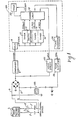
- FIG. 1 of the drawings shows a block diagram detailing the interconnection of the present control device with the telephone line of a subscriber, over which line control signals are transmitted to and from a central telephone office.
- Each one of a possible plurality of (e.g. either Touch Tone or rotary dial) telephones, which are interconnected to form a user telephone network 1, is connected to a subscriber line.
- the subscriber line typically includes a pair of conductors 2 and 2', designated TIP and RING.
- Each conductor is associated with a respective hook switch 3 and 3', so that hook flash control signals can be transmitted thereover.
- the aforementioned telephone control device includes a circuit which is interconnected with the subscriber's line to enable a telephone user to place an existing call in a hold condition without disconnecting the caller, so that the call can be resumed at a later time and/or from a different (i.e. a telephone extension) location.
- the hold circuit is adapted to be selectively actuated when the telephone user initiates a particular sequence of hook flash signals by depressing and then releasing the hook switches 3 and 3'.
- the sequence of signals that will actuate the hold circuit hereof comprises a pair of successively generated hook flash signals.
- each hook flash signal is greater than approximately 150 milliseconds, but less than approximately 750 milliseconds.
- sequence comprising the pair of hook flash signals must be completed within a particular time (e.g. 4 seconds) interval. It is to be understood that the above- identified sequence of hook flash signals and the timing constraints applied thereto are but a preferred example of a pulse train that is suitable to actuate the present hold circuit. However, the hold circuit hereof could be modified to be responsive to other hook flash signal sequences.
- the pulse duration of a single hook flash signal must be long enough (e.g. at least 150 milliseconds) to distinguish a hook flash hold control signal from each of a dial pulse (such as that which is generated when dialing a rotary dial telephone) and rapid, repetitive on-hook signals that are used to signal the telephone operator.
- the pulse duration of the hook flash signal must also be short enough (e.g. less than 750 milliseconds) to distinguish a hook flash hold control signal from an on-hook signal that is generated when the hook switches are depressed, whereby to disconnect an existing call.
- the pair of hook flash signals must be completed within a suitable time interval (e.g. 4 seconds) to distinguish an intended hold operation from an inadvertent operation of the telephone hook switch. That is, the user is provided with the ability to change his mind and thereby terminate a hold command by not completing the particular sequence of hook flash signals within the prescribed time interval.
- the presently disclosed control device includes a conventional diode bridge rectifier 4, opposite ends of which are connected to circuit lines 5 and 5'.
- Circuit lines 5 and 5' are interconnected with the TIP and RING conductors 2 and 2' of the subscriber's line at the user telephone network 1 in a manner to be better described while referring to FIG. 2, hereinafter.
- a third end of bridge rectifier 4 is connected to supply an input signal to an electrical comparator 6.
- Comparator 6 may comprise a conventional semiconductor chip, such as that having chip number LM 311 manufactured by National Semiconductor Corporation. Comparator 6 is utilized to sense the voltage acri l ss the circuit lines 5 and 5'.
- Comparator 6 is adapted to provide an output signal (designated SWHOOK) having either one of two signal levels, depending upon the disposition of the hook switches 3 and 3' and the corresponding voltage between lines 5 and 5'.
- the output SWHOOK signal from comparator 6 is applied to a conventional signal delay means 8.
- Delay means 8 is mechanized according to conventional techniques, so as to introduce a particular delay (e.g. 150 milliseconds) in the time in which a signal can be transmitted therethrough.
- the time delay introduced by delay means 8 corresponds to the minimum hook flash signal pulse width, as defined above.
- the output signal (designated OFHOOK) of delay means. 8 is applied to respective input terminals of each of a plurality of timers 10, 14, and 16 and a digital differentiator 12.
- the first timer 10 may comprise a conventional semiconductor chip such as that having chip number NE 555 manufactured by National Semiconductor Corporation.
- Timer 10 is triggered by the output OFHOOK signal from delay means 8, and, as is best illustrated in FIG. 4, is adapted to provide a logical true or relatively positive output signal level (designated ENABLE) approximately one second after the telephone handset is removed from it cradle and switches 3 and 3' are released.
- the output signal of timer 10 remains logically true until slightly more than one second after the telephone handset is returned to its cradle where the hook switches are depressed.
- timer 10 provides a logical false or relatively negative output signal level.
- the purpose of timer 10 is to eliminate the possibility of an accidental or false hold condition. Such a condition could occur as a result of either of a bouncing hook switch (during the removing or replacing of the handset at the telephone cradle) or a voltage change that is applied to the telephone circuits immediately prior to and during the generation of a ring signal thereat.
- the output ENABLE signal from timer 10 is supplied to a control logic block 18, the details of which will be described hereinafter when referring to FIG. 3.
- Digital differentiator 12 may comprise a conventional semiconductor chip, such as one half of chip number 74123 manufactured by National Semiconductor Corporation. Digital differentiator 12 is triggered by the output OFHOOK signal from delay means 8 and is adapted to generate an output signal consisting of a one shot control pulse having a relatively true logic level whenever the handset is removed from its cradle and hook switches 3 and 3' are released. The one shot output signal from digital differentiator 10 is supplied to the control logic 18 in order to the reby set or release the logic for controlling the actuation of the hold circuit which forms the present telephone control device.
- the second timer 14 may comprise a conventional semiconductor chip, such as one half of the aforementioned chip number 74123.
- Timer 14 is triggered by the output OFHOOK signal from delay means 8 and is adapted to generate an output signal (designated FLASH-DELAY) consisting of a one shot control pulse.
- the one shot control pulse has a relatively true logic level whenever the handset is returned to its cradle or when hook switches 3 and 3' are depressed for longer than 150 milliseconds.
- the FLASH-DELAY output signal from timer 14 is supplied to the control logic 18.
- the . pulse width (e.g. approximately 750 milliseconds) of the output signal from timer 14 is utilized by the control logic 18 to distinguish between an intentional hook switch control flash and an attempt by a user to hang up and thereby disconnect an existing call.
- the third timer 16 may comprise a conventional semiconductor chip such as one half of the aforementioned chip number 74123.
- Timer 16 is triggered by the output OFHOOK signal from delay means 8 and, as is best illustrated in FIG. 4, is adapted to generate an output signal (designated 4SEC) having a relatively true logic level and a pulse width of approximately 4 seconds shortly after the handset is returned to its cradle or when switches 3 and 3' are depressed.
- the output signal from timer 16 is supplied to the control logic 18 in order to prevent a false hold condition, such as that which could occur when the second hook flash of the aforementioned two flash sequence occurs later than 4 seconds after the generation of the first flash or when the second flash is not generated at all. More particularly, the output signal from timer 16 is utilized to reset a portion of the control logic 18 in the event that the prescribed hook flash signal sequence is not completed within a 4 second time interval.
- Timer 20 may comprise a semiconductor chip such as that formed by the interconnection of one half of chip number NE 556 with chip number 7493, each of which chips being manufactured by National Semiconductor Corporation.
- timer 20 is triggered by the HOLDFF output signal from logic 18 immediately after the completion of the prescribed hook flash signal sequence, whereupon timer 20 generates an output signal having a relatively true logic level.
- the output signal of timer 20 is fed back to reset a portion of control logic 18 so as to thereby automatically terminate a hold condition whenever the length of the hold condition exceeds the duration of the timer output signal.
- the pulse width of the output signal from timer 20 is selected to be of convenient length (e.g. approximately 6 minutes). Hence, by virtue of timer 20, the user's telephone circuits can be reset to receive new incoming calls in the event that the user forgets to terminate a hold condition for longer than 6 minutes.
- Another output terminal from the control logic 18 is connected to supply an output signal (designated HOLD) therefrom to a hold circuit 22.
- the hold circuit which will be described in greater detail hereinafter when referring to FIG. 2, may be selectively actuated whereby to enable a telephone user to return the telephone handset to its cradle while temporarily (for less than 6 minutes) placing an existing call in a hold condition, so that the call can be resumed from a later time and/or a different location.
- the hold circuit is actuated after the prescribed hook flash signal sequence has been completed and the user returns the telephone handset to its cradle, whereby to depress hook switches 3 and 3'.
- An output terminal of control circuit 22 is connected to an electrical junction between bridge rectifier 4 and signal comparator 6.
- tone generator 24 may comprise a conventional semiconductor chip, such as that formed by the interconnection of one and one half chips, each having number NE 556 and being manufactured by National Semiconductor Corporation.
- the output signal (designated TONE) of tone generator 24 is an audible signal that can be heard by both the maker and recipient of a telephone call, whereby to indicate that the call is being placed in a hold condition.
- the output TONE signal is supplied from tone generator 24 to a conventional tone amplifier 26, the details of which will be described in greater detail when referring hereinafter to FIG. 2. Accordingly, an amplified audio output signal is coupled to circuit lines 5 and 5' by means of a conventional audio output transformer 28.
- timers 10, 12, 14, 16 and 20, the control logic 18, and tone generator 24 could be mechanized as part of a single microprocessor chip 100 suitably programmed to accomplish the desired functions.
- a single microprocessor chip 100 suitably programmed to accomplish the desired functions.
- an available single chip microprocessor having application herein in chip number COP 411 manufactured by National Semiconductor Corporation.
- comparator 6 typically comprises a high gain amplifier 32 having a pair of input terminals by which the telephone line voltage can be compared with a reference voltage (approximately 5 volts dc), designated V cc .
- High gain amplifier 32 is adapted to switch at approximately 15 volts dc so that the level of the output signal therefrom supplied to chip control block 100 is suitable to provide an indication as to the disposition of the telephone hook switches (either released or depressed).
- Telephone hold circuit 22 is interconnected between an output terminal 33 of chip control block 100 and a common electrical junction 34 formed between diode bridge 4 and the voltage comparator 6. More particularly, hold circuit 22 comprises the interconnection of a current limiting resistor 36, a Z ener diode 38, the conduction path of a NPN transistor device 40, and a source of reference potential, such as ground. Current limiting resistor 36 is selected so as to simulate the dynamic impedance of the telephone when the circuits thereof are rendered in a hold condition.
- Zener diode 38 is a readily available device such as Part No. lN4744 manufactured by National Semiconductor Corporation. Zener diode 38 has a breakdown voltage of approximately 15 volts dc.
- Transistor switch 40 is also a readily available device, such as that having Part No. 2N6719, manufactured by National Semiconductor Corporation.
- the base electrode of transistor switch 40 is connected to terminal 33 through a current limiting resistor 42.
- the source of supply of reference voltage V cc is also connected to terminal 33 through a conventional pull up resistor 43.
- Zener diode 38 functions to distinguish between an off-hook condition (i.e. where the hook switches are released) and a hold condition (where the telephone handset is returned to its cradle so as to depress the hook switches). More particularly, Zener diode 38 is biased by the voltage at common electrical junction 34.
- electrical junction 34 is driven to a substantially higher voltage (approximately 50 volts) when the telephone hook switches are depressed relative to the voltage (approximately 6 volts) thereat when the hook switches are released. Accordingly, Zener diode becomes forward biased so as to be rendered in a conductive condition whenever the telephone hook switches are depressed (i.e. when the telephone handset is returned to its cradle). Moreover, Zener diode 38 is back biased so as to be rendered in a non-conductive condition whenever the hook switches are released (i.e. such as when the telephone handset is removed from its cradle). Transistor switch 40 is rendered conductive when the base thereof receives a relatively true logic level signal from the output terminal 33 of chip control block 100.
- the telephone circuits are rendered in a hold condition when Zener diode 38 and transistor switch 40 are each rendered in a conductive condition, whereby to clamp electrical junction 34 close to ground through the respective conduction paths thereof.
- hold circuit 22 is actuated only when the telephone hook switches are depressed or the telephone handset is returned to its cradle and when a relatively true logic level signal (designated HOLD in F I G. 1) is applied to transistor switch 40 from an output terminal 33 of chip control block 100.
- Tone amplifier 26 comprises a Zener diode 44 and any suitable NPN transistor switch 46.
- Zener diode 44 and transistor switch 46 are conventional devices.
- transistor 46 may be part No. 2N3904 manufactured by National Semiconductor Corporation.
- the conduction path of Zener diode 44 is connected across the conduction path of transistor switch 46 between a common electrical junction 48 and a source of reference potential, such as ground.
- Zener diode 4 4 functions to protect transistor switch 46 from transient voltages that could occur when ringing signals are applied to the subscriber's line.
- An output signal (designated TONE in FIG. 1) is applied from chip control block 100 to the base of transistor switch 46 through a current limiting resistor 47, so as to control the conductivity thereof.
- the output terminal (i.e. electrical junction 48) of tone amplifier 26 is connected through a blocking compacitor 50 to one end of a first winding which forms audio output transformer 28.
- the second end of the first winding is connected to a source of reference potential, such as ground.
- One end of a second winding of audio output transformer 28 is connected to circuit line 5, and the other end of the second winding is connected through a blocking capacitor 52 to the circuit line 5'.
- Audio output transformer 28 is of conventional design, such as that characterized by 250 ohm-8 ohm transformer windings.
- Audio output transformer 28 functions to couple an audio signal from the output terminal 48 of tone amplifier 26 to the circuit lines 5 and 5', so as to enable both the caller and recipient of a telephone call to receive an output signal whereby to indicate that the telephone circuit is being rendered in a hold condition.
- the circuit lines 5 and 5' of the present telephone control device are connected to a well-known modular plug 30.
- Modular plug 30 may be inserted into a jack socket of a conventional telephone adapter (not shown).
- Another modular telephone plug (not shown) is connected to receive the TIP and RING conductors 2 and 2' from the subscriber's line.
- the last-mentioned modular telephone plug may be inserted into a different jack socket of the aforementioned telephone adapter.
- the telephone adapter can then be easily installed within a suitable recepticle which is typically located at the rear of the telephone housing.
- the present telephone control device may be conveniently connected at the subscriber's line with each telephone that forms the subscriber's telephone network.
- the subscriber's telephones need not be re-wired or modified as has typically occurred with many prior art telephone control circuits.
- modular telephone plug 30 can be eliminated, so that circuit lines 5 and 5' can be hard wired directly to the conductors which form the subscriber's telephone line.
- the output signal from timer 10 (of FIG. 1) is applied to a conventional inverter 50.
- the output signal (designated ENABLE) from inverter 50 is applied to one input terminal of a 2-input AND gate 52 and to one input terminal (designated J) of a conventional JK flip-flop 56.
- the output signal (designated FLASH-DELAY) of timer 14 is applied to a second input terminal of AND gate 52.
- the output terminal from AND gate 52 is connected to one input terminal of a 2-input terminal AND gate 54, to one input terminal (designated J) of another JK flip-flop 70, and to the input terminal of an inverter 62.
- An output terminal (designated Q) of flip-flop 70 supplies an output signal (designated 1FLASH) to the second input terminal of AND gate 54.
- the output terminal of AND gate 54 is connected to each of a second input terminal (designated J) of flip-flop 56, and to one input terminal of a 2-input terminal AND gate 58.
- the output signal from the digital differentiator 12 (of F I G. 1) is applied to each of the second input terminal of AND gate 58 and to a clock terminal (designated CLK) of flip-flop 56 so as to provide synchronous control thereof.
- the output terminal of AND gate 58 is connected to the input terminal of an inverter 60.
- the output terminal of inverter 60 is connected to an input terminal of the tone generator 24.
- the output signal from timer 20 is applied to the input terminal of an inverter 68.
- the output signal of inverter 68 is applied to a clearing terminal (designated CLR) of flip-flop 56, the energization of which is suitable to reset flip-flop 56.
- One output terminal (designated Q) of flip-flop 56 is connected to supply an output signal (designated H OL D FF) to one of the chips that forms timer 20.
- a second output terminal (designated Q') of flip-flop 56 is connected to supply an output signal to each of the second chip which forms timer 20 and to one input terminal of a 2-input terminal AND gate 64.
- the output signal of inverter 62 is applied to the second input terminal of AND gate 64.
- the output signal of AND gate 64 is applied to an inverter 66.
- the output signal (designated HOLD) of inverter 66 is applied to the hold circuit 22 (best shown in FIG. 2).
- the output signal from the digital differentiator 12 is also applied to a clock terminal (designated CLK) of flip-flop 70, so as to provide synchronous control thereof.
- the output signal (designated 4SEC) from timer 16 (of FIG. 1) is applied to a clearing terminal (designated CLR) of flip-flop 70 in order to reset flip-flop 70.
- a relatively positive source of reference potential, V is applied through a current limiting resistor to each of an input terminal (designated PR) of flip-flop 56 and to respective input terminals (designated PR and K) of flip-flop 70.
- JK flip-flops 56 and 70 may be mechanized from conventional semiconductor chips, such as chip No. 74109 manufactured by National Semiconductor Corporation, one half of which being utilized to implement flip-flop 56 and the other half of which being utilized to implement flip-flop 70.
- each of the logic gates described above is mechanized by conventional transistor-transistor logic (TTL) techniques.
- TTL transistor-transistor logic
- FIG. 4 illustrates the output signal levels, relative to time, of certain components which form the present telephone control device when the hold circuit 22 thereof is actuated and a telephone call is placed in a hold condition.
- hold circuit 22 can be actuated and latched whenever the hook switches 3 and 3' are flashed so as to produce a sequence of two hook flash signals within a 4 second interval.
- a hook flash signal is defined by the depression of hook switches 3 and 3', so that the output signal (designated SWHOOK) from comparator 6 has a relatively false logic level for an interval of time greater than 150 milliseconds but less than 750 milliseconds.
- the SWHOOK signal 72 has a relatively true logic level (e.g. +5 volts dc) whenever the telephone handset is removed from its cradle and hook switches 3 and 3' are released.
- the SWHOOK signal has a relatively false logic level (e.g. ground) during the generation of hook flash signals 74 and 76.
- the user After the prescribed sequence of hook flash signals 74 and 76 is generated, the user returns his telephone handset to its cradle, at which point 77 in time the SWHOOK signal again has a relatively false logic level and the hold circuit 22 becomes actuated and latched. Hold circuit 22 will remain latched for a maximum of 6 minutes after the generation of the second hook flash signal until the user either removes the handset from its cradle (whereby to resume a telephone conversation) or when the 6 minute timer 20 times out, so as to reset flip-flop 56 and thereby automatically terminate the hold condition.
- timer 20 times out, so as to provide a signal to both reset flip-flop 56 (at the CLR input terminal thereof) and cause the deactivation of hold circuit 22 (via AND gate 64) by means of a relatively true logic level signal that is subsequently provided at the Q' output terminal of flip-flop 56.
- Certain warning signals generated from the central telephone office may also terminate the hold condition.
- flip-flop 56 is set at the end of the second hook flash signal 76, so as to provide the output signal HOLDFF having a relatively true logic level 94 by which to trigger 6 minute timer 20.
- the output signal OFHOOK from delay means 8 is delayed by an interval 78 of approximately 150 milliseconds relative to the generation of the SWHOOK signal from comparator 6.
- the OFHOOK signal has a relatively false logic level 150 milliseconds after the hook switches are depressed (i.e. on-hook) and the SWHOOK signal correspondingly goes to a false logic level.
- the OFHOOK signal has a relatively true logic level (at substantially the same time as the SWHOOK signal) when the hook switches are subsequently released (i.e. off-hook).
- the SW H OOK signal In order for the OFHOOK signal to have a relatively false logic level, the SW H OOK signal must be continuously false for at least 150 milliseconds.
- the delay means 8 functions as a timer to establish a lower time limit (e.g. 150 milliseconds), the duration of which must be exceeded by a hook flash signal in order that the particular sequence thereof can be properly completed.
- the output ENABLE signal from inverter 50 (the signal level of which is inverted relative to that of the output signal supplied from timer 10) has a relatively true logic level after the OFHOOK signal has had a relatively true logic level continuously for one second.
- the ENABLE signal has a relatively false logic level after the OFHOOK signal has had a relatively false logic level continuously for one second. Therefore, any transient change in the level of the OFHOOK signal acts to reset the one second delay in the ENABLE signal.
- the aforementioned one second intervals are represented by the reference numerals 80 and 82, respectively.
- hold circuit 22 may be actuated only when the ENABLE signal has a relatively true logic level.
- the FLASH-DELAY output signal from timer 14 provides one shot pulses 86 and 88 having a relatively true logic level whenever the hook switches are depressed for longer than 150 milliseconds.
- the generation of one shot pulses 86 is delayed by a 150 millisecond interval (designated by reference numeral 84) relative to the generation of the SWHOOK hook flash signals 74 and 76 of FIG. 4a.
- the FLASH-DELAY signal therefore produces 750 millisecond delays which time respective hook flash signals. Accorrdingly, in the event that a hook flash signal exceeds 750 milliseconds (e. g.
- timer 14 times out, so that a relatively false FLASH-DELAY signal is subsequently supplied to both deactivate hold circuit 22 (via AND gates 52 and 64) by a corresponding relatively false HOLD signal and to maintain the logical state of flip-flops 56 and 70 (by grounding the respective J input terminals thereof).
- the 4SEC output signal from 4 second timer 16 has a relatively true logic level 90 approximately 150 milliseconds after the generation of the first ⁇ .ook flash signal 74.
- the 4SEC signal has a width of 4 seconds, whereupon a relatively false signal is thereafter assumed. Therefore, and in the event that the sequence of hook flashes 74 and 76 is not completed within the 4 second interval of the 4SEC signal, a relatively false logic level signal is applied from timer 16 to the CLR input terminal of flip-flop 70, whereby to reset flip-flop 70 to be responsive to a newly initiated hook flash signal sequence.
- the flip-flop 70 supplies an output signal (designated 1 FLASH) from an output terminal Q thereof to an input terminal J of flip-flop 56 via AND gate 54.
- the 1 FLASH output signal has a relatively true logic level at the completion of the first hook flash signal 74.
- Flip-flop 70 is set via AND gate 52 when receiving a relatively true logic level pulse at an input terminal J thereof when the first hook flash signal 74 is generated. Therefore, flip-flop 70 stores an indication that a first hook flash signal has occurred.
- the flip-flop 56 is set via AND gate 54 by a relatively true logic level signal at the J input terminal thereof when the second hook flash signal is generated within the 4 second interval (established by 4 second timer 16).
- an output signal from output terminal Q' of flip-flop 56 is applied to the hold circuit 22 via AND gate 64 and inverter 66.
- the output signal, designated HOLD, of inverter 66 has a relatively true logic level 150 milliseconds after the first hook flash is generated (i.e. when the OFHOOK signal assumes a relatively false logic level).
- circuit 22 assumes a momentary hold condition, until it can be determined whether a second hook flash signal has been generated or the telephone handset has been otherwise returned to its cradle whereby to enable the user to terminate an existing call.
- the HOLD signal assumes a relatively false logic level (designated 98) 150 milliseconds after the completion of the first hook flash signal 74.
- the HOLD signal again assumes a relatively true logic level when the second pulse 86 of the FLASH-DELAY signal is applied to AND gate 52.
- the user returns his telephone handset to its cradle, at which point (designated 102) in time the Zener diode 38 and transistor 40 of hold circuit 22 are rendered conductive by the relatively true level of the HOLD signal, whereupon hold circuit 22 is actuated and latched (by means of flip-flop 56) in order to place an existing call in a hold condition for a maximum of 5 minutes.
- the hold condition is also released whenever the user removes his handset from its cradle or when the OFHOOK signal assumes a relatively true logic level while the ENABLE assumes a relatively false logic level.
- a tone burst 103 or audible signal (designated TONE) is generated by tone generator 24.
- the tone burst preferably comprises sixteen 50 millisecond pulses of a 2 kHz squarewave. The interval between pulses is approximately 100 milliseconds, so that the envelope is square.
- the tone burst may be generated with the hold circuit 22 actuated and latched, so that an additional audible signal is applied whenever an attempt is made to place an existing call in a hold condition.
- FIG. 5 of the drawings illustrates the output signal levels, relative to time, of some of the components which form the present hold device when an improper hook flash signal sequence is initiated (e.g. because of an accidental depression of the hook switches), so that the hold circuit 22 is not actuated and an existing call is not rendered in a hold condition. More particularly, and referring concurrently to FIGs. 1-3 and 5, after the telephone handset has been removed from its cradle and hook switches 3 and 3' are released, the SWHOOK signal has a relatively true logic level 104. However, only a single hook flash signal 106 is generated within a 4 second interval of time. Accordingly, the FLASH-DELAY signal includes only a single one shot pulse.
- the output signal HOLDFF from flip-flop 56 never attains a relatively true logic level, inasmuch as the second hook flash signal is not generated before flip-flop 70 is reset by the 4SEC output signal from timer 16.
- the 4SEC and 1 FLASH signals may assume either one of relatively true or false logic level signals 110 or 112 and 114 or 116, respectively, depending upon the amount of time (relative to 4 seconds) before the handset is returned to its cradle.
- the HOLD signal has a relatively true logic level only during 750 millisecond intervals after the hook switch is depressed and a momentary hold condition is assumed.
- the HOLD signal has a relatively false logic level, so that the transistor switch 40 of hold circuit 22 is not rendered conductive. Consequently, hold circuit 22 is not actuated, so that the telephone user, rather than placing an existing call in a hold condition, as was described when referring to FIG. 4, otherwise terminates the existing call when his handset is returned to its cradle.
Landscapes
- Engineering & Computer Science (AREA)
- Signal Processing (AREA)
- Sub-Exchange Stations And Push- Button Telephones (AREA)
- Telephone Function (AREA)
- Coin-Freed Apparatuses For Hiring Articles (AREA)
- Selective Calling Equipment (AREA)
- Telephone Set Structure (AREA)
Applications Claiming Priority (2)
| Application Number | Priority Date | Filing Date | Title |
|---|---|---|---|
| US273807 | 1981-06-15 | ||
| US06/273,807 US4387274A (en) | 1981-06-15 | 1981-06-15 | Hook flash signal actuated telephone control device |
Publications (2)
| Publication Number | Publication Date |
|---|---|
| EP0067268A2 true EP0067268A2 (de) | 1982-12-22 |
| EP0067268A3 EP0067268A3 (de) | 1983-08-10 |
Family
ID=23045486
Family Applications (1)
| Application Number | Title | Priority Date | Filing Date |
|---|---|---|---|
| EP82100128A Withdrawn EP0067268A3 (de) | 1981-06-15 | 1982-01-11 | Steuereinrichtung für Fernsprechapparat betätigt durch ein Kurzzeitunterbrechungssignal vom Hakenumschalter |
Country Status (9)
| Country | Link |
|---|---|
| US (1) | US4387274A (de) |
| EP (1) | EP0067268A3 (de) |
| JP (1) | JPS58500964A (de) |
| AR (1) | AR229693A1 (de) |
| BR (1) | BR8109032A (de) |
| CA (1) | CA1182231A (de) |
| DK (1) | DK47483A (de) |
| NO (1) | NO830507L (de) |
| WO (1) | WO1982004516A1 (de) |
Cited By (5)
| Publication number | Priority date | Publication date | Assignee | Title |
|---|---|---|---|---|
| GB2160744A (en) * | 1984-05-10 | 1985-12-24 | Nitsuko Ltd | Exchange line holding circuit |
| EP0176291A3 (de) * | 1984-09-21 | 1988-03-30 | Alcatel N.V. | Tastengegensprechanlage mit verteilter Steuerung |
| EP0355488A3 (de) * | 1988-08-18 | 1991-07-31 | Siemens Aktiengesellschaft | Verfahren zur Durchführung einer Steuerprozedur im Zusammmenhang mit der Herbeiführung eines Haltezustandes einer Leitung in einem rechnergesteuerten Kommunikationssystem insbesondere einem Key-Kommunikationssystem |
| FR2664773A1 (fr) * | 1990-07-11 | 1992-01-17 | Sebty Sarl | Dispositif pour conserver une communication telephonique etablie tout en raccrochant le combine du poste en service. |
| EP0603436A1 (de) * | 1992-12-21 | 1994-06-29 | Sgs-Thomson Microelectronics Pte Ltd. | Schaltung zur Detektion eines Parallelfernsprechgerät |
Families Citing this family (26)
| Publication number | Priority date | Publication date | Assignee | Title |
|---|---|---|---|---|
| US4492822A (en) * | 1982-09-30 | 1985-01-08 | Alderman Robert J | Telephone hold circuit with improved self-limiting amplifier for injecting an audio signal during hold conditions |
| US4435622A (en) | 1982-11-01 | 1984-03-06 | Gte Automatic Electric Inc. | Latching relay hold circuit for a telephone instrument |
| US4454385A (en) * | 1982-11-01 | 1984-06-12 | Gte Automatic Electric Inc. | Latching relay hold release circuit for a telephone instrument |
| US4440981A (en) * | 1982-11-26 | 1984-04-03 | Gte Automatic Electric Inc. | Electronic hold circuit |
| US4447674A (en) * | 1982-11-26 | 1984-05-08 | Gte Automatic Electric Inc. | Electronic hold release circuit |
| US4492823A (en) * | 1983-05-02 | 1985-01-08 | Gte Business Communication Systems | Dual timing circuit for telephone subscriber's instrument |
| US4674118A (en) * | 1985-03-25 | 1987-06-16 | Tie/Communications, Inc. | Telephone line hold and hold release apparatus |
| EP0313562B1 (de) * | 1986-06-30 | 1993-04-21 | FORBES, Anthony | Fernsprechgerät mit wartestellung |
| DE3725329A1 (de) * | 1987-07-30 | 1989-02-09 | Siemens Ag | Schaltungsanordnung fuer eine digitale fernsprechstation |
| JPH03162160A (ja) * | 1989-11-21 | 1991-07-12 | Nippon Telegr & Teleph Corp <Ntt> | フッキングパルス検出装置 |
| US5539812A (en) * | 1992-07-29 | 1996-07-23 | Kitchin; Dwight W. | Method and apparatus for detecting an attempted three-way conference call on a remote telephone |
| DE4334288A1 (de) * | 1993-10-08 | 1995-04-13 | Deutsche Bundespost Telekom | Schutzvorrichtung gegen irrtümliches Unterlassen des Ausschaltens eines Ein/Aus-Schalters bei Fernsprechapparaten |
| DE4427600A1 (de) * | 1994-08-04 | 1996-03-07 | Deutsche Telekom Ag | Verfahren zum Auslösen einer Identifizierung des Anschlusses eines rufenden Teilnehmers |
| US5768355A (en) * | 1996-05-16 | 1998-06-16 | Science Dynamics Corporation | Three-way call detection system |
| US5832075A (en) * | 1996-09-20 | 1998-11-03 | Mitel Corporation | Off-hook detector for headset |
| US6351525B1 (en) | 1998-09-22 | 2002-02-26 | Telefonaktiebolaget L M Ericsson (Publ) | Method and apparatus for conservation of switching exchange resources |
| US6947546B2 (en) * | 2000-09-26 | 2005-09-20 | Ceglia Michael J | Hook-flash simulation in parallel with off-hook devices |
| US8000269B1 (en) | 2001-07-13 | 2011-08-16 | Securus Technologies, Inc. | Call processing with voice over internet protocol transmission |
| US7899167B1 (en) | 2003-08-15 | 2011-03-01 | Securus Technologies, Inc. | Centralized call processing |
| US7505406B1 (en) | 2001-07-13 | 2009-03-17 | Evercom Systems, Inc. | Public telephone control with voice over internet protocol transmission |
| US7916845B2 (en) | 2006-04-13 | 2011-03-29 | Securus Technologies, Inc. | Unauthorized call activity detection and prevention systems and methods for a Voice over Internet Protocol environment |
| US9026468B2 (en) | 2002-04-29 | 2015-05-05 | Securus Technologies, Inc. | System and method for proactively establishing a third-party payment account for services rendered to a resident of a controlled-environment facility |
| US7860222B1 (en) | 2003-11-24 | 2010-12-28 | Securus Technologies, Inc. | Systems and methods for acquiring, accessing, and analyzing investigative information |
| US9020114B2 (en) | 2002-04-29 | 2015-04-28 | Securus Technologies, Inc. | Systems and methods for detecting a call anomaly using biometric identification |
| US7529357B1 (en) | 2003-08-15 | 2009-05-05 | Evercom Systems, Inc. | Inmate management and call processing systems and methods |
| US10796392B1 (en) | 2007-05-22 | 2020-10-06 | Securus Technologies, Llc | Systems and methods for facilitating booking, bonding and release |
Family Cites Families (14)
| Publication number | Priority date | Publication date | Assignee | Title |
|---|---|---|---|---|
| US3114801A (en) * | 1959-06-15 | 1963-12-17 | Itt | Multi-line telephone station |
| US3551606A (en) * | 1968-02-21 | 1970-12-29 | Stephen H Chapman | Electronic key telephone |
| US3629514A (en) * | 1970-02-02 | 1971-12-21 | G T E Automatic Electric Lab I | Subscriber{40 s holding circuit |
| US3825693A (en) * | 1972-09-25 | 1974-07-23 | Tele Resources Inc | Time division multiplex branch exchange |
| DE2436256A1 (de) * | 1974-07-27 | 1976-02-05 | Licentia Gmbh | Schaltungsanordnung zur zusaetzlichen zeichengabe |
| US4011413A (en) * | 1976-01-12 | 1977-03-08 | Gimix, Inc. | Hold circuit for telephone |
| DE2651209A1 (de) * | 1976-11-10 | 1978-05-11 | Merk Gmbh Telefonbau Fried | Schaltungsanordnung zum internruf bei kleinen nebenstellenanlagen mit zwei sprechstellen |
| US4086440A (en) * | 1977-04-12 | 1978-04-25 | Chestel, Inc. | Telephone set with loop current interruption timing control |
| US4090038A (en) * | 1977-07-14 | 1978-05-16 | Bell Telephone Laboratories, Incorporated | Audio signal on hold circuit |
| US4196317A (en) * | 1978-01-20 | 1980-04-01 | Bartelink E H B | Telephone intercom system |
| US4251693A (en) * | 1978-08-03 | 1981-02-17 | Christiansen Gary F | Fixed impulse generator for hook switch flash |
| US4243844A (en) * | 1978-09-19 | 1981-01-06 | Waldman Herbert H | Hold circuit for telephone system |
| US4313037A (en) * | 1980-06-02 | 1982-01-26 | Rolm Corporation | Telephone station set with improved flash signalling |
| US4311880A (en) * | 1980-11-10 | 1982-01-19 | Bell Telephone Laboratories, Incorporated | Key telephone hold arrangement |
-
1981
- 1981-06-15 US US06/273,807 patent/US4387274A/en not_active Expired - Fee Related
- 1981-12-18 JP JP82500549A patent/JPS58500964A/ja active Pending
- 1981-12-18 BR BR8109032A patent/BR8109032A/pt unknown
- 1981-12-18 WO PCT/US1981/001721 patent/WO1982004516A1/en not_active Ceased
-
1982
- 1982-01-11 EP EP82100128A patent/EP0067268A3/de not_active Withdrawn
- 1982-01-19 CA CA000394459A patent/CA1182231A/en not_active Expired
- 1982-02-26 AR AR288589A patent/AR229693A1/es active
-
1983
- 1983-02-04 DK DK47483A patent/DK47483A/da not_active Application Discontinuation
- 1983-02-15 NO NO830507A patent/NO830507L/no unknown
Cited By (6)
| Publication number | Priority date | Publication date | Assignee | Title |
|---|---|---|---|---|
| GB2160744A (en) * | 1984-05-10 | 1985-12-24 | Nitsuko Ltd | Exchange line holding circuit |
| EP0176291A3 (de) * | 1984-09-21 | 1988-03-30 | Alcatel N.V. | Tastengegensprechanlage mit verteilter Steuerung |
| EP0355488A3 (de) * | 1988-08-18 | 1991-07-31 | Siemens Aktiengesellschaft | Verfahren zur Durchführung einer Steuerprozedur im Zusammmenhang mit der Herbeiführung eines Haltezustandes einer Leitung in einem rechnergesteuerten Kommunikationssystem insbesondere einem Key-Kommunikationssystem |
| FR2664773A1 (fr) * | 1990-07-11 | 1992-01-17 | Sebty Sarl | Dispositif pour conserver une communication telephonique etablie tout en raccrochant le combine du poste en service. |
| EP0603436A1 (de) * | 1992-12-21 | 1994-06-29 | Sgs-Thomson Microelectronics Pte Ltd. | Schaltung zur Detektion eines Parallelfernsprechgerät |
| US5394465A (en) * | 1992-12-21 | 1995-02-28 | Sgs-Thomson Microelectronics, Pte Ltd. | Parallel phone detection circuit |
Also Published As
| Publication number | Publication date |
|---|---|
| WO1982004516A1 (en) | 1982-12-23 |
| AR229693A1 (es) | 1983-10-31 |
| CA1182231A (en) | 1985-02-05 |
| BR8109032A (pt) | 1983-05-31 |
| JPS58500964A (ja) | 1983-06-09 |
| NO830507L (no) | 1983-02-15 |
| EP0067268A3 (de) | 1983-08-10 |
| DK47483D0 (da) | 1983-02-04 |
| US4387274A (en) | 1983-06-07 |
| DK47483A (da) | 1983-02-04 |
Similar Documents
| Publication | Publication Date | Title |
|---|---|---|
| US4387274A (en) | Hook flash signal actuated telephone control device | |
| US3997731A (en) | Apparatus for custom calling features in a telephone system | |
| US4243844A (en) | Hold circuit for telephone system | |
| US4769837A (en) | Device for adding intercom functions to a phone system | |
| US5142569A (en) | Apparatus for selectively enabling subscriber device to respond to ringing signal in dependence upon ringing cadence | |
| US3742151A (en) | Communication call holding and supervising circuit | |
| US4169220A (en) | Telephone instrument connection block with remotely actuated line test | |
| US3870822A (en) | Supplying a charging current by way of telephone lines or the like | |
| US4132860A (en) | Hold control for a key telephone system | |
| US3829619A (en) | Telephone ring trip circuit | |
| US5870458A (en) | Automatic facsimile/data/voice switch | |
| US3764752A (en) | Telephone line card system | |
| USRE31643E (en) | Hold circuit for telephone system | |
| US3784756A (en) | Subscriber loop range extender | |
| US5392327A (en) | Termination unit with maintenance facility | |
| US3420963A (en) | Communication system line circuit particularly for key telephone systems | |
| US4496797A (en) | Circuit for automatically connecting and disconnecting a speakerphone to a telephone line | |
| US4133985A (en) | Key telephone system | |
| US4031332A (en) | Telephone ringer insolator | |
| US4896352A (en) | Telephone set circuit including an overvoltage protection | |
| CA1049672A (en) | Key telephone system line circuit | |
| US4440981A (en) | Electronic hold circuit | |
| US4313037A (en) | Telephone station set with improved flash signalling | |
| AU8085482A (en) | Hook flash signal actuated telephone control device | |
| US5131031A (en) | Hold circuits for telephone systems |
Legal Events
| Date | Code | Title | Description |
|---|---|---|---|
| PUAI | Public reference made under article 153(3) epc to a published international application that has entered the european phase |
Free format text: ORIGINAL CODE: 0009012 |
|
| AK | Designated contracting states |
Designated state(s): AT BE CH DE FR GB IT LI LU NL SE |
|
| PUAL | Search report despatched |
Free format text: ORIGINAL CODE: 0009013 |
|
| AK | Designated contracting states |
Designated state(s): AT BE CH DE FR GB IT LI LU NL SE |
|
| 17P | Request for examination filed |
Effective date: 19840208 |
|
| STAA | Information on the status of an ep patent application or granted ep patent |
Free format text: STATUS: THE APPLICATION IS DEEMED TO BE WITHDRAWN |
|
| 18D | Application deemed to be withdrawn |
Effective date: 19850610 |
|
| RIN1 | Information on inventor provided before grant (corrected) |
Inventor name: STEIN, JEFFREY D. Inventor name: MCCOOL, JOHN M. |