EP0067304A2 - Verarbeitungsnetz und Verfahren zur physischen Planung von in sehr hohem Grad integrierten Schaltkreisen - Google Patents
Verarbeitungsnetz und Verfahren zur physischen Planung von in sehr hohem Grad integrierten Schaltkreisen Download PDFInfo
- Publication number
- EP0067304A2 EP0067304A2 EP82103941A EP82103941A EP0067304A2 EP 0067304 A2 EP0067304 A2 EP 0067304A2 EP 82103941 A EP82103941 A EP 82103941A EP 82103941 A EP82103941 A EP 82103941A EP 0067304 A2 EP0067304 A2 EP 0067304A2
- Authority
- EP
- European Patent Office
- Prior art keywords
- array
- cell
- net
- cells
- wiring
- Prior art date
- Legal status (The legal status is an assumption and is not a legal conclusion. Google has not performed a legal analysis and makes no representation as to the accuracy of the status listed.)
- Granted
Links
Images


















Classifications
-
- G—PHYSICS
- G06—COMPUTING OR CALCULATING; COUNTING
- G06F—ELECTRIC DIGITAL DATA PROCESSING
- G06F30/00—Computer-aided design [CAD]
- G06F30/30—Circuit design
- G06F30/39—Circuit design at the physical level
- G06F30/394—Routing
Definitions
- the invention is in the field of physical design of large scale integrated (LSI) and very large scale integrated (VLSI) circuits, and especially of the interconnections and wire routings between the circuits formed on a chip.
- apparatus is set forth for determining the wire routings in a LSI or VLSI circuit structure comprised of cells, wherein the cells are composed of electronic devices functioning as a logic gate: groups of cells may be interconnected to function as flip flops, shift registers and the like.
- a supervisory controller communicates with n, where n is an integer, identical multi-port processors, with one processor dedicated to each cell, for determining the wire routings between the respective cells.
- Each processor communicates simultaneously with its 4 adjacent neighbor processors to determine channel routings from one point to the next in the array of cells, wherein a channel routing includes vertical and horizontal paths. Following determination of global channel routings, exact vertical and horizontal tracks for the wire paths are assigned, and then overflow routing is considered. Timing analysis, placement, shape generation and checking may also be obtained from the apparatus by a judicious use of its parallel computation power in appropriate manners.
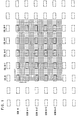
- a master-slice chip consists of an array of active circuit areas on one plane with wiring channels running between these active areas in orthogonal directions on separate planes. Pins or vias running orthogonally to both planes are used to effect connections between the planes.
- the part of the physical design automation system which determines the appropriate routing of the various wires in the system is termed the wiring operation.
- the wiring operation contains a few steps which are repeated a significant number of times, and these operations invariably involve a large number of instructions in the conventional CPU. Due to the frequency of these operations, the speed of wiring can be improved considerably if these specific operations are speeded-up. In view of these circumstances, the wiring calculations may be performed efficiently and economically by utilizing a special purpose high-speed machine having the characteristics of being capable of performing many operations in parallel and performing repetitive operations which slow the wiring operation performance of a CPU by specialized hardware implemented in each of a plurality of processing elements.
- It is still a further object of the invention to provide an improved global wiring machine for VLSI networks comprised of master-slice chips consisting of an array of active circuit areas on one plane with wiring channels running between these active areas in orthogonal directions on separate planes, with vias running orthogonally to both channels to affect connections between the planes.
- the VLSI physical design machine is array structure composed of a plurality of microprocessor-like special processing elements (SPEs) arranged in an n by n matrix corresponding to a master-slice chip image. That is, there is a SPE associated with each cell of the chip. Each SPE corresponds to a channel intersection and adjacent active components on the master-slice chip. Each SPE contains both logic as well as memory components, and hence is a microprocessor-like element. Unlike a conventional- general purpose microprocessor, each SPE has built into its hardware those specialized functions corresponding to the sequences of instructions on a general purpose machine which are performed repeatedly. Thus, the element can be designed to perform each sequence in minimum number of machine cycles, preferably one such cycle. By custom design, a SPE can be designed as a single VLSI chip with about 100 pins and a cycle time of 100 nanoseconds or less. Each SPE communicates only with its four adjacent neighboring SPEs in addition to the supervisory control unit.
- SPE microprocessor-like
- the supervisory control over the array of SPEs may be either hierarchical or global. In the former, groups of local SPEs communicate with an element of a smaller array of controlling elements which in turn communicate among each other and to a high controlling mechanism. In the global scheme, all the SPEs directly communicate with a central supervisor which controls the loading and unloading of information as well as task assignment. The central supervisor must be able to broadcast as well as address individual or groups of elements.
- U. S. Patent No. 4,093,990 to Koller et al sets forth an exemplary method of producing mass patterns for integrated circuits composed of standard cells.
- the cells are first grouped in a predeterminable number of cell groups in such a way that as few connections as possible extend between the groups, and the space requirement of the individual groups is equal.
- U. S. Patent No. 3,653,070 to Hill et al sets forth a method of producing art work for a logic circuit to be fabricated by printed circuit board techniques.
- the art work is produced by a data processing machine programmed to run a package routing, a placement routine and a routing routine in addition to check routines.
- U. S. Patent No. 4,215,401 to Holsztynski et al relates to digital array processors of the type having a plurality of identical interconnected cells which perform sequential transformation operations on data matrices under the control of a central processor and more particularly to unique forms of cell construction and interconnection between the processing cells.
- the array processor set forth is a single instruction multiple data flow.(SIMD) machine, which communicates with its 4 neighbors by sequential shift registers, thus not allowing simultaneous access.
- Control is centralized rather than autonomous on an individual basis as required for VLSI design. Internal nodes in the array cannot be independently selected, that is, there is no independent X/Y select mechanism. Therefore, the array of procesors described, would not be useful in VLSI or physical design.
- U. S. Patent No. 3,979,728 to Reddaway sets forth an array processor, operative as the peripheral of a conventional computer. Each processing element is organized on a bit-serial basis, with single-bit registers and a bit- addressable store, and the array is controlled by a microprogrammed main control unit.
- Reddaway is a SIMD machine like Holsztynski et al. Reddaway selects one row and one column in the array at a time, rather than multiple column and row selection at a given time.
- SIMD processing apparatus has been described in the SOLOMON computer .(Slotnick et al., Fall Joint Computer Conference 1962, page 97; Gregory et al., IEEE Transactions on Electronic Computers, December 1963, page 774).
- This apparatus consists of an array of relatively simple processing elements, each of which is arranged to perform arithmetic operations upon input data in a bit-serial manner.
- ILLIAC IV Computer Barnes et al., IEEE April 1972, page 369.
- apparatus is set forth determining the wire routings in a VLSI circuit structure comprised of cells, in which a plurality of routes for a plurality of nets is considered concurrently, with the consequence of a given path being considered relative to the routability of other paths by performing congestion estimates.
- a supervisory unit communicating with an array of identical multi-port processors with one processor dedicated to each cell in a VLSI chip.
- Each processor operating in an MIMD mode communicates simultaneously with its 4 adjacent neighborhood processors, to concurrently perform congestion estimates and to determine channel routings from one point to the next in the VLSI array, wherein a channel routing includes vertical and horizontal paths.
- Method and apparatus is set forth for physical design of large scale integrated circuit structure comprised of an array of logic elements.
- a supervisory device communicates with an array of identical multi-port processing means, with one such processing means being dedicated to each logic device for determining the wire routing between the various logic elements.
- Each processing means communicates simultaneously with its 4 adjacent neighboring processing means to perform various computations to determine such things as channel routings from one.point to another in the array, wherein a channel routing includes vertical and horizontal paths. Following the determination of optimal channel routings, vertical and horizontal exact paths are determined next, with overflow routings then being considered.
- a system of multi-port processors is set forth in conjunction with a supervisory unit, which is used to interconnect an array of logic devices that have been formed on a substrate.
- a supervisory unit which is used to interconnect an array of logic devices that have been formed on a substrate.
- LST logic service terminals
- This logic device, and the other devices in the array may be a register, flip flop, gate network such as a NAND, OR, NOR or the like.
- the device illustrated could be a three input NAND device or some other device that has 4 terminals.
- the number of terminals is exemplary, as some logic devices may have more or less than 4 terminals.
- each logic device there is a provision for.horizontal and vertical wire tracks in successive layers.
- a layer of insulation Directly above the logic service terminal is a layer of insulation.
- vertical wires may be deposited as needed by the circuit. If any of the logic service terminals on the logic device need to be connected to the vertical conductors, a vertical pin or via is formed, thus joining a vertical wire through the insulation to logic service terminal. While the vertical wires are numbered from 0 - 7, it is to be understood that this number is only exemplary and that the number of vertical wires may be less or greater than shown.
- Another layer of insulation is laid down so that the horizontal conductors can be deposited on top of this second layer of insulation.
- a channel here refers to a plurality of wiring tracks associated with a logic device in the array.
- the tracks 0-7 constitute a vertical channel of the chip illustrated in FIG. 1; and the tracks A, B, C and D constitute a horizontal channel.
- a device and its adjoining channel intersection has 4 boundaries, and such a bounded grid region is termed a cell of the array.
- a cell is identified by its row and column positions in the arrays.
- SPE multi-port processor
- the operation of the SPEs will be described in detail shortly.
- Each SPE communicates with the supervisory machine which is called the "controller”.
- the controller provides each SPE with information that it needs, and when each cell has completed its function as set forth by the controller, the controller then receives information from the cell. How SPEs determine the wiring paths connecting various logic service terminals will be described later.
- each cell in the array is composed of horizontal and vertical channels and an active circuit component at each intersection of channels.
- Each channel has a specified number of wire tracks on which the signal wires must be routed between the respective circuit components to respective LSTs.
- Each cell has 4 boundaries with the neighboring cell, and the resulting bounded grid region is termed a cell.
- One SPE represents one such cell as set forth in the general scheme.
- the most important step in wiring such a chip is the global channel allocation for every net to.be wired.
- a net is defined as those terminal points that are to be made electrically common by wire connections.
- the global wiring routes all nets through available channels regardless of which specific track a given wire is to be assigned.
- the main constraint of the global allocation process is the channel capacity, that is, the available number of tracks at each cell boundary.
- the goal is to route all nets without violating the channel capacity and to minimize the total wire length.
- There are additional goals such as to maximize the remaining channel capacity, i.e., to even out the track usage, if possible, to facilitate the follow-on processes of exact track assignments.
- the global wiring is accomplished utilizing a non-linear-cost maze running process which is to be described later.
- the global routing process finds a best cost route from the source wire to the sink points, within a detour limit (d) plus the shortest reachable distance.
- Physical design refers to the technique by which the design of a digital system represented by interconnected logic gates is converted to patterns for a set of masks to be used in fabricating a chip or a set of chips for the system.
- Tools for physical design generally take the form of software packages aiding the various steps of the conversion. The three common separate, though by no means unrelated, steps are partitioning, placement and wiring.
- Partitioning refers to the process by which portions of a large design are allocated to different chips when a single chip cannot contain the entire design.
- the placement process places the components of a chip, commonly gates, within the chip. Often, the positions where these components may be placed are a set of well-defined slots, separated from each other by areas through which wires or metal segments may be run in order to interconnect the components.
- a gate-array or a master-slice chip.
- the algorithms used to allocate the space between the components for the interconnection are contained in the wiring package.
- Each computer consists of a processor, a memory unit, one port to each of its adjacent computers (four, except at the boundaries) and a link to an additional computer which is called the controller.
- X- and Y-select lines make it possible for the controller to access any desired node or some subset of nodes in the array.
- the memory of each node computer carries the complete information about a corresponding circuit cell in an n x n sized master-slice chip. While such a conglomeration of computers would have been unthinkable just a few years ago, the advent of microprocessor makes such a scheme inexpensive and practical today.
- An 8 x 8 array of computers for example, each of which consists of a commercial 8-bit microprocessor, 2 kilobytes of memory and auxiliary circuit enabling neighbor and controller communication can be utilized for the wiring function.
- the controller is also an 8-bit microprocessor with 48 kilobytes of memory, floppy and hard disk units, printer, terminal and a link to the host computer system of the facility. The following details the steps in performing the wiring.
- An 8 x 8 array can also be programmed to wire a chip having more than 64 components.
- Global wiring is the name given to the phase of wiring in which wires are allocated to channels in the chip, without specifically assigning tracks within the channel. The latter assignment is accomplished subsequently by an exact embedding algorithm.
- each node computes the total number of tracks available in each of four directions. It is also provided with a list of nets which have a terminal in that node. (A net is a set of two or more terminals which have to be connected together.)
- the process just described determines the shortest path between the source and any sink, choosing the path with the least cost if there is more than one. It achieves this in time proportional to the rectilinear distance between the source and the-nearest sink. When the placement is good, this distance grows very slowly as the chip size increases. In fact, a reasonable estimate for this distance even for a 10,000 circuit chip is 5. However, the number of nets to be wired is approximately a linear function of the chip size, leading us to conclude that the time for the entire process as described is approximately a linear function of the chip size.
- detour Any deviation from the shortest path between a source and a sink is termed a detour.
- the nets which are laid down early are not necessarily laid in shortest paths. Rather, they are allowed to detour whenever they reach an area which should preferably be avoided so that future nets do not get blocked in. This can be achieved by the following modification to the above procedure.
- each node instead of quitting (sending the arbitrarily large value to its neighbors) after sending one meaningful value, now quits after sending d + 1 meaningful values. (Note that a blockage at a port could cause the port cost itself to be very high. As a result, if no sink is reached, the net is kept aside for wiring later. However, once a node starts sending meaningful values, it is not possible for it to send a higher value at any of the subsequent d time steps.) Each node also maintains a table indicating the direction from which it received the best value against the time step at which that value arrived.
- the direction at the previous step is preferred, whenever possible. (This simply helps in getting the shortest path whenever there are paths of different lengths having the same minimum total cost.)
- the backtrace process is initiated by the sink with the minimum cost prompting the neighbor in the direction stored against its last active time step, say t. While prompting its neighbor, it also sends the value t-1 to the neighbor.
- the neighbor in turn refers to its table and prompts its neighbor in the direction stored against the time step t-1, along with the value t-2. This process continues until, as before, the sink is reached.
- the time taken was less than 2 seconds of real time.
- the program connected all the nets in the minimum Steiner connection when the detour limit, d was set to 0.
- the nets took longer paths, but the channel capacity remaining at the end of the run showed a uniform spread over the entire chip. This demonstrates the fact that when nets are allowed to detour, they do so in such a way as to make the wiring of future nets easier. This proves to be quite helpful for the exact embedding phase which follows global wiring. It was also observed that at the end as the channel demand reduced due to fewer remaining nets, the nets were wired with minimum Steiner length.
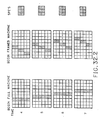
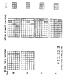
- edges of the computer array can be connected in a wrap-around fashion, so that the nodes at the north edge had the nodes at the south edge as their north neighbors, the nodes at the east edge had the nodes at the west edge as their east neighbor, and so on.
- the folding process performs better than the first method because it takes advantage of the relatively high locality in the distribution of node computation activity without sacrificing the resolution of the wiring process.
- a node computer must retain the circuit data for every eighth circuit cell in the horizontal direction and in the vertical direction. This suggests a requirement for increased memory requirement at each node.
- the process described here is more accurately a cut-and-stack process, rather than a strict accordion-type folding process. The latter process, while feasible, and while free of the wrap-around hardware requirement, carries with it the inconvenience of alternating directions for consecutive frames.
- the exact embedding process follows the global wiring process.
- each node must allocate exact tracks to the nets which have been assigned to it by the global wiring phase.
- the algorithm begins by making a complete assignment for the circuit cell in the center of the chip.
- the tracks assigned to the nets which cross the boundary of the cell are sent to the appropriate neighboring processing elements, which accommodate this data in making assignments for its circuit cell. This process continues in a diamond shaped wavefront form until the tracks at the circuit cells at the corners of the chip have been allocated.
- FIG . 2 is a block diagram representation of the .physical design machine according to the present invention.
- a host system for example, an IBM 370 computer, 10 is connected to a mask generating machine 12 and to a system bus 14 via a serial I/O bus interface 16.
- a printer 18 may also be be connected to the interface card 16 to receive inputs from the system bus 14.
- a control processor 20 is connected to the bus 14 and to a console 22.
- a controller memory 24, is also connected to the bus 14.
- Direct access storage devices (DASDs) 26 are connected to the system bus 14 via a bus adapter 28.
- the central processor 20 communicates with a processor array 30 comprised of SPEs 32 via an array I/O processor 34.
- the processor array 30 is comprised of an n by n array of the SPEs 32 which are equal in number to the cells set forth in FIG. 1, or a submultiple thereof with the system of FIG. 2 accomplishing the wire routing of the cells.
- All communications between the control processor 20 and the processor array 30 are accomplished by a memory mapping technique. That is, all communication from the controller 20 to the array 30 is accomplished by the controller writing into special memory addresses which are intercepted by the array I/O processor 34 and further routed to their final destinations. Likewise, the SPEs 32 in the array 30, communicates with the controller 20 by writing into their own special memory address which causes appropriate routing of the messages by hardware therein.
- the SPE to SPE communication is implemented using the same techniques as will be set forth in detail later.
- the processor array 30 is composed of rows and columns of SPEs each of which communicates with its 4 adjacent neighbors, North, South, East and West, as well as with the controller 20 through special bus mechanisms. It is to be appreciated that any arbritrary number of rows N and columns M can be implemented in the practice of the invention.
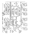
- FIGS. 3.1 and 3.2 form a detailed block diagram representation of the array I/O processor 34 which contains as a part the logic hardware to process the protocol of the system bus interfacing.
- the processor 34 includes special registers memory mapped from the controller 20 as well as other logic to drive and control the processor array 30.
- the controller 20 selects the SPEs or a given SPE by setting the X and Y, column and row respectively, select bits.
- the controller 20 composes two bit vectors for an X select register and a Y select register where a logical 1 means the column and/or the row corresponding to the bit position is selected.
- An SPE considers itself selected if and only if there is a conjunction of both the column and row selection signals. Therefore, the controller 20, by writing into the memory mapped locations that is the X select registers and the Y select registers have the ability to select the group of SPEs corresponding to the cross-and-product of the two register contents.
- the SPEs in the array are complete slaves of the controller 20 in the sense that it is only the controller which can decide to which group of SPEs it wishes to transmit and/or receive information from.
- the SPEs that are not selected by the mechanisms of X-Y coincident selection, cannot participate in any communication, be it data, control or address. If the controller wishes to communicate with all SPEs, say broadcast to all or listen from everyone, it merely sets both the X and Y select registers to all 1's before any further action.
- the array I/O processor 34 is connected to the system bus 14, for provision of bidirectional address, data and system bus service signals.
- Data signals are provided to and from bidirectional bus 36, and to a data bus 38 and from there to the X select register 40, the Y select register 42, and data drivers 44.
- Data is provided to data bus 36 from the data bus 46 which receives X responses from column 1 through column m of the array via OR gates 48, 50 and 52 respectively.
- Y responses are provided from row 1 through row n of the array via OR gate 54, 56 and 58 respectively.
- Data from the array data bus from all SPEs is provided via OR gates 60, and service bus signals are provided from all the SPEs via OR gates 61.
- Address signals are provided from the system bus 14 to an address bus 62 and from there to array I/O control logic network 64 and drivers 66.
- System bus and memory service signals are provided from the systems bus 14 to systems bus interface logic network 68 via bus 70.
- the select signals provided to registers 40 and 42 are in turn provided via drivers 72 and 74 respectively as column and row select signals to the SPEs in the array, and data signals are provided from the drivers 44 to the SPEs in the array.
- Control logic signals are provided via a bus 76 from control logic 64 to drivers 78 as control signals to the SPEs in the array.
- the address signals on bus 62 are provided by the driver 66 to address all of the SPEs in the array.
- the address signal bus 62 various types of operations are performed by memory mapped operations. Firstly, some portions of these signals constitute the actual memory location in each of the SPEs in the array where the local memory of every SPE is identically addressed, and the distinction as to which of these local memories are addressed is governed by the X select register 40 and the Y select register 42. Secondly, some portions of these address signals signify that the address is a special memory mapped location some of which reside within the processor 34 and some in the individual SPEs.
- the array I/O control logic 64 under the supervision of the usual system bus interface logic 68 decodes the incoming address signals on bus 62 to control various data control signal paths within the processor 34 and in the array.
- the essential locations and the corresponding usages of address is set forth in detail later. How this decoding and controlling is performed is well known in the art and therefore will not be set forth in detail.
- Table 1 below sets forth the logical functions performed by the array I/O control logic 64.
- FIG. 4 is a schematic diagram representation of a . driver 80 which is utilized for each individual bit in the drivers 44, 78 and 66 of FIG. 3.2.
- the driver 80 receives a bit K for each bit on the signal line on an input line 82, which bit is gated in response to an enable signal 84 from control logic 64 for providing the bit on an output line 86, with this bit being fanned-out to each SPE in the array.
- the driver 80 can be composed of a fan-out tree of drivers to share the driving load, as is well known to those skilled in the art.
- FIG. 5 illustrates SPE 32, including the control and data inputs to and therefrom to neighboring SPEs and the array I/O processor.
- the ORing data bus 88 is connected to the output of the drivers 44 and 60, the address bus 90 is connected to the drivers 66, the control bus 92 is connected to the driver 78 and the service bus 94 is connected to the input of the OR gate 62 of the processor 34 as set forth in FIG. 3.2.
- Each SPE communicates with its adjacent North, South, West and East neighbors with certain communication signals being provided per SPE.
- a Strobe OUT signal is provided on each line 96, a Flag IN signal on each line 98, a Strobe IN signal on each line 100, a Flag OUT signal on each line 102, neighborhood Data IN is provided IN on each line 104 and neighborhood Data OUT is provided on each line 106.
- X and Y select signals are provided on lines 108 and 110 respectively per column and row to all of the SPEs, with the X select being provided on line 112 to the SPE 32 shown, and the Y select being provided on line 114.
- X and Y response signals are provided on lines 116 and 118 respectively from the SPE 32 to X response and Y response lines for the array on lines 120 and 122 respectively.
- the neighbor communication lines to North, South, East and West neighbors are identical to all SPEs except for the SPEs at the North, South, East and West boundaries of the array. These boundary SPEs consider the cells opposite the array as their neighbors in the outward direction from the array viewpoint.
- the detail functional operation of the SPE 32 is set forth below relative to FIGS. 6.1 and 6.2 and flcwcharts which follow.
- FIGS. 6.1 and 6.2 is a current mode embodiment of detailed block diagram representation of the SPE 32.
- the control bus signal on line 92 is provided to SPE control logic network 124 via a control buffer 126, with the control bus signal being provided from the buffer 126 via lines 128 and 130 to AIN latch 132 and AOUT latch 134 respectively.
- the X select and Y select signals 114 and 112 respectively are also applied as inputs to logic network 124.
- the address bus signals on bus 90 are provided to an external address buffer 136.
- the ORing data bus line 88 is connected to buses 138, 140, 142 and 144 for connection to IN register 146, OUT register 148, data IN buffer 150 and data OUT buffer 152 respectively.
- the service bus 94 is connected to a service buffer 154 and to a service word 156 via a bus 158.
- the service word network 156 besides including the latches 132 and 134, includes a service latch 159.
- the service word 156 is connected to the SPE data bus 160 via a bus 161.
- the Strobe IN signals on the respective lines 100 are connected to a North IN Flag latch 162N, an East IN Flag latch 162E, a South IN Flag latch 162S and West IN Flag latch 162W, respectively. These latches provide Flag OUT signals on the respective.lines 102, with these signals also being provided to a bus 168 for application to a Flag buffer 170.
- the neighbor Flag IN signals on the respective lines 98 are also applied to the bus 168 for application to the Flag buffer 170, with the output of the Flag buffer being provided to the SPE data bus 160.
- the Strobe signals OUT are provided on the respective lines 96 from the SPE control logic network 124.
- the neighbor data IN signals on the respective 104 lines are provided to a North IN latch 172N, an East IN latch 172E, a South IN latch 172S and a West IN latch 172W.
- the outputs from these latches are provided to the SP E data bus 160.
- the data bus 160 is connected to the input of a neighbor data OUT buffer 180, with the neighbor data OUT buffer 180 providing the respective neighbor data OUT signals on the respective lines 106.
- the SPE control logic network 124 is connected to microprocessor 182 via a bidirectional bus 184.
- the microprocessor 182 may, for example, be one of any number of commercially available microprocessors such as the Zilog Z80.
- the microprocessor 182 provides addresses to an address buffer 186 via a bus 188 and exchanges data. with a data buffer 190 via a bidirectional bus 192.
- the output of the address buffer 186 is connected to the SPE address bus 194 which is also connected tc. a local memory 196, which for example may be a random access memory (RAM).
- the address bus 194 is also connected to the output of the buffer 136 via a bus 198 and to an address input of the SPE control logic network 124 via a bus 200.
- the local memory 196 is connected to the SPE data bus 160 via a bidirectional bus 202.
- the registers 146, 148, and the buffers 150 and 152 are also connected to the data bus 160 via buses 204, 206, 208 and 210 respectively.
- the latches 172, 174, 176, 178 and the buffer 180 are connected to the data bus 160 via buses 212, 214, 216, 218 and 220 respectively.
- the SPE control logic network 124 functions as the main data routing mechanism within the SPE 32, to the global controller 20 and to the adjacent neighbor SPEs.
- the global communication lines, 92 through buffer 126, 90 through buffer 136, 88 through I/O registers 146 and 148 and through buffers 150 and 152, and 94 through buffer 154 are all gated by the X-Y selection mechanism within SPE control logic 124.
- the X - Y selection mechanism within logic 124 is as illustrated in FIG. 7.
- An AND gate 222 receives the X select and Y select signals on lines 114 and 112 respectively, and upon detecting coincidence, an enable signal is provided on output line 224 that is distributed to all the global buffers and registers of the SPE 32 as set forth above. All global communications as set forth below are also governed by this selection mechanism.
- the reset signal which is a part of the control signals on line 92 through the buffer 126 resets the microprocessor 182.
- the microprocessor 182 dictates the protocols of local buses 194 and 160. Therefore, some of the control signal lines 92 from the controller 20 via the array I/O processor 34, are dedicated to commercially specified local bus handling which is processed and/or routed via.signal lines 184 to the microprocessor 182 by the SPE control logic 124 in a well known manner. These signals, for example, usually include bus acknowledge and bus request signals as well as others.
- the control signal lines 92 also include the usual microprocessor control commands such as, interrupt, reset and the like, as well as the SPE local memory read, write command lines, which signal functions are well understood in microprocessor technology.
- the microprocessor 182 is temporarily interrupted and the buses 194 and 160 are given to the global tasks which take precedence over local tasks.
- Two of the control signal lines of 92, namely the lines 128 and 130 are dedicated to setting the protocol bits for the I/O register use through the global data bus 94.
- the signal line 128 sets the AIN latch 132 to a logical 1 and the signal 130 resets the AOUT latch 134 to logical 0.
- SPE control logic 124 In response to the global commands from the I/O processor, is set forth below.
- control logic 124 recognizes the global request for the local buses, the external address buffer 136 is enabled for providing the address to the bus 194, after a temporary interrupt for the duration of the task. Then, the control logic 124 decodes the address it receives from the bus 194 by way of the bus 200 and takes appropriate data routing operations as set forth in Table 2 below.
- the SPE communicates with its adjacent neighbor SPE's through the data ports 104 and 106 respectively in each of the North, South, East and West directions.
- the Flag latches 162(N,E,S,W) the neighbor Flag-IN on the lines 98, Strobe-OUT signals on the lines 96, Flag-OUT 102, and the Strobe-IN signals 100 are used. The use of these signals and latches and their actions are described later.
- SPE control logic 124 The following sets forth the data routing of the SPE control logic 124. Internal requests are issued from the microprocessor 182 in the form of DMA to the various SPE latches, registers and ports, as well as the SPE local memory 196. All of these requests are preceded by usual local bus protocol handled by the control logic 124 via bus 184 from the microprocessor 182. Table 3 below sets forth the actions taken by control logic 124 for internal data routing purposes.
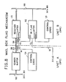
- FIG. 8 sets forth a neighbor communication mechanism which is known in the art variously known as a mail box flag protocol or a request and acknowledge protocol.
- the mechanism is one of the many possible methods which may be used to ensure the data integrity when two processors transfer data without the receiving processor anticipating the data at the time of transfer.
- the mail box flag mechanism operates on the same principle as the mail box mechanism for the AIN latch 132 and AOUT latch 134 set forth in FIG. 6.1.
- the units A and B shown in FIG. 8 can be either North-South neighboring SPEs or East-West neighboring SPEs, or to a generic extent may be representative of an SPE and the array I/O processor 34, insofar as the I/O registers 146 and 148 (FIG. 6.1) communication is concerned. With reciprocal symmetry in mind, the case is considered where unit A transmits to unit B.
- the unit A includes the data bus 160, a sender buffer 180 and logic network 124.
- Unit B is shown as including a receiver latch 172 and IN flag latch 162 and the logic network 124 as well as the data bus 160. Communications between the sender buffer 180 and the receiver latch 172 are via the buses 213 and 104.
- the operation of the mail box flag mechanism is according to the steps set forth below.
- the control logic 124 While the SPE control logic 124 is in charge of routing the SPE internal and external data movements, the control logic 124 does so only by the command of either the array I/O processor 34 or the microprocessor 182.
- the actual processing of data and ordering of the data movement in the SPE is carried out by this microprocessor 182. That is, the calculations and functions to be carried out by the SPEs in conjunction with other SPEs in parallel, under the supervision of the controller, by programming means using various available instructions and data stored in the SPE local memory 196.
- Some of the special instructions contemplated, such as simultaneous 4 port communication and arithmetic and logical operations, are emulated by the commercial microprocessor standard instruction set.
- the SPE may incorporate some or all of the special hardware instructions of 4 port nature. Regardless of what instruction set is utilized, it is well understood in the programming art of digital processors that implementing a program is a skilled but routine art once the flow of functional operation is envisioned and specified.
- System reset is accomplished at the control processor 20 of FIG. 2 by a hardware switch which causes the processor to jump to a fixed address in a read only memory.
- the read only memory is programmed to load necessary controller and the SPE application programs from the DASDs into the memories 24 and 196.
- the X-Y select registers 40 and 42 of FIG. 3.1 contain a vector of all 1's. If any X-Y subset is desired for any operations, such subset vectors are composed by the controller and stored in the X-Y select registers 40 and 42, before any further action takes place.
- Determination of responding SPEs is accomplished by the controller reading the memory mapped special location, the X-Y response lines.
- the controller first reads the X response of the entire array and finds what columns of the array are responding. For each responding column, the controller selects the column and all rows and reads the Y-response line to determine exact location of each responding SPE in that column. As the controller finds a responding S P E location it can perform operations on it such as reading a certain value in SPE memory or the I/O register and operate on them.
- SPE memory loading is accomplished by the controller bringing the program or data from the DASDs or directly from its main memory and loading into all SPE memories simultaneously by the DMA mechanism previously described.
- the common portion of data and program can be loaded onto any group of SPEs selectable as a cross product of the X-Y selection vector.
- Communication using the I/O registers of SPE is distinguished from DMA into the SPE memories, in that the DMA into the SPE memory temporarily interrupts the SPE operations due to the SPE local bus usage for the DMA action, while the I/O registers can be used without disturbing the SPE local bus.
- the SPE is notified of data handling being put into the I/O register or read from there by the controller, through the AIN and AOUT Flag mechanisms previously set forth. The controller sets these status bits by simply reading and writing into the selected SPE I/O registers while it can observe the status by reading the service word as described earlier.
- the SPEs are initiated by the controller writing data to special DMA address for resetting the array.
- the array I/O processor decodes this address and energizes the control signal line designated for reset which resets the selected SPE's microprocessors.
- the instruction in the location 0 causes a jump with proper index into the jump table that contains the beginning points of various programs stored in the SPE local memory.
- the proper index into the jump table can be DMAed to the fixed SPE memory location by the controller or it can be stored there by the SPE in anticipation of the next execution sequence beginning.
- Intra array communication is carried out by sending and receiving the data between the neighboring SPEs.
- a mechanism of how the sending and receiving is accomplished was previously set forth. It is understood that each SPE contains a special memory location where the boundary status is stored. Thus, each SPE is cognizant of the fact that there is or is not a neighboring SPE in any specific direction. Whenever the program flowchart specifies a neighborhood communication, the SPE first confirms the existence of a neighboring SPE before the action of either transmitting or receiving. The boundary SPEs then simply omit the step of transmitting or receiving to the empty direction, in exception to general description in the flowchart.
- a synchronization mechanism is achieved by the service word of the SPE being used to report all SPE status, the most important of which is the job completion status.
- all SPEs can set a prearranged bit position to be logical 1, signifying the busy status.
- the SPE reads the service word, resets the bit to logical 0 and stores back to the service word.
- the service bus being the ORing bus that ORs all the service words of selected SPEs to the array I/O processor, the bit will be a logical one as long as any of the selected SPEs are busy and will be a logical 0 only if all of the selected SPEs have completed the task.
- the controller thus determines the completion of all of the SPEs before it directs the array for the next subprocess.
- the placement and wiring can be a combined process in some applications.
- the final output of the physical design process serves as input to the actual physical realization of the logic packages at the manufacturing plant by a mask generation machine or other lithographic system such as indicated at 12 in FIG. 2.
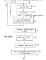
- the wire routing process 230 of FIG. 9 is set -forth in more detail in FIG. 10.
- the placement process for components 228 preceding this process determines what logic element is placed at what position of the chip, and what terminals of these logic elements are connected to what terminals of the other logic elements.
- a global routing process is undertaken as indicated at logic block 234 to determine optimal channel routings between logic service terminals.
- an exact embedding of horizontal and vertical wires to tracks within the selected channel is undertaken as indicated at logic block 236.
- overflow handling and checking is accomplished as indicated at logic block 238, with the process then returning to point 232 as indicated in FIG. 9.
- a chip generically known in the industry as a master-slice chip or a gate array chip in the LSI/VLSI range is utilized.
- the master-slice chip 240 shown in FIG. 11 is comprised of rows and columns of cells 242. Passing through the cells are horizontal channels 244 composed of a plurality of wiring tracks 246 in the horizontal direction, and vertical channels 248 composed of a plurality of wiring tracks 250 in the vertical direction.
- the horizontal and vertical wiring channels are said to be in their respective wiring planes which are separated by an insulating layer as previously set forth. Active logic elements reside underneath these two wiring planes separated by yet another insulating layer.
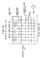
- FIG. 12 shows in detail a cell 242 which can be construed as the combination of a logic device 252 and the corresponding horizontal and vertical channel intersection.
- the four imaginary boundaries of the cells are called N , E, S, W ports.
- the number of available wiring tracks on each port is called the channel capacity.
- the logic device 252 in each cell is a collection of active semiconductor logic devices that is personalized to perform the elementary logic functions such as AND, OR, NAND, NOR, NOT, EX-OR, latch, and the like. Logic functions placed at the site dictate how the logic device is personalized, and this is not pertinent to the wire routing process. Depending upon what function is assigned to the logic device 252, however, there are fixed locations called the logic service terminals 254 along the vertical wiring tracks 250.
- LSTs may be placed along the horizontal tracks 246, by means which are not pertinent to the method to be described, that must be connected to other cell LSTs similarly assigned.
- the personalization of the logic device, outside of the wiring process, may thus use some portions of the horizontal and vertical wiring tracks, which manifest themselves as blockages in the affected tracks. Therefore, the channel capacity in North and South ports may not be the same, and likewise in the East and West directions.
- a net refers to the collection of LSTs in the placed cells to be made electrically common by connected wires laid along the wiring track.
- a wire When a wire must change its direction it does so by changing the wiring plane by using a via programmed at the intersection 256 of horizonal and vertical wiring -tracks.
- the chip input-output pins connect to driver and receiver cells which are located at some designated position. Usually these cells are along the periphery of the chip, but many other arrangements are practiced.
- the technology also dictates configurations of vias within a cell.
- the constraint usually manifests itself as a prohibition of certain adjacent vias being used along the tracks. More detailed analysis of how this constraint is handled can be found in the IB M Journal of Research and Development, July 1981, in an article entitled, "Number of Vias a Control Parameter for Global Wiring of High Density Chips" by D. T. Lee et al.
- VIAMIN refers to the minimal guaranteed number of vias that can be configured within the cell without violating the technology constraint.
- the number VIAMAX refers to the maximum number of vias that can be assigned within the cell under the most advantageous configuration. That is, no more than VIAMAX vias can possibly be assigned to the cell, i.e., no more than 'VIAMAX bending wires can be routed through the cell.
- the wire routing process begins with the placement and chip geometry data.
- the placement data provided by 228 (Fig. 9), is a net list which provides for each net to be routed: (A) the number of all LSTs, (B) the cell position of each of the LSTs and (C) the exact LST physical location within the cells.
- the chip geometry consists of information concerning the blockage status of each cell and the channel capacity of all the ports of all the cells.
- the first and most important major step in the wire routing process 230 is called the global routing 234.
- the routes of all the nets are globally determined in cell resolution.
- the exact LST locations, the exact tracks of the route, or the exact position of the vias within the cells are ignored at this step.
- the follow-on step 236 then embeds the globally routed wire segments to exact tracks within the channels while satisfying the detailed technology constraints in fine resolution. Should any wire segment be left as an overflow from the previous two step procedure, an overflow handling step 238 is invoked.
- Current practice in the art is that most of the overflows are manually embedded causing a long delay in the total development time of the chip. It is a further aim of this invention to minimize the overflows and to .automatically process at high speed, the overflows that do occur.
- FIG. 13 is a flowchart illustrating the global routing process set forth in logic block 234 of FIG. 10.
- Net data, channel capacity and detour limit is provided as indicated to flowchart logic block 260 wherein the first step is undertaken to estimate the congestion at each port, that is each cell boundary of the chip, due to the anticipated use of tracks by the wire routes.
- the process then routes one net at a time as indicated at logic blocks 262, 272 and 276 or alternatively the order of nets to be wired may be determined by some other suitable procedure replacing the simple order of processing the nets as indicated at 262, 272 and 276.
- the congestion estimate contributed by the net is subtracted as indicated at logic block 264, thereby reflecting only the estimated congestion due to the nets that have not as yet been routed.
- a cost for a crossing (COST) is developed as indicated at logic block 266 for each of the cell boundaries.
- the cost for bending a wire in the cell called the via cost is also determined for each cell during the process indicated at logic block 266.
- the process then continues as indicated at logic block 268 to determine the minimum cost route to connect the net by use of the processor array system. If the wiring process is successful as determined at logic block 270, the process continues to . logic block 272 where the net number, I, is incremented.
- the logic block 274 records an overflow, and continues to logic block 272 and 276 where the question is asked, "Are all nets done?" If the answer is no, the process returns to logic block 264 and continues as previously set forth for the next net. If all nets are done, the process exits as indicated at 278.
- FIG. 14 depicts the general flow of the congestion estimation process 260 of FIG. 13.
- Net data is provided as indicated at 280 with the estimate being initialized to zero as indicated at logic block 282.
- the congestion estimate value of a given net is determined at logic block 286, wherein two reasonable assumptions are made. First, that the wire would be most likely to follow the shortest possible route, and secondly that two point connections would likely contain at most two bends rather than multiple zigzag paths.
- logic block 288 the accumulation of values at every cell boundary takes place. It is noted that the same subprocess at logic block 286 is used along with subtraction replacing the 288, for the embodiment of 264 as indicated in FIG. 13.
- the logic blocks 290 and 292 together control the sequencing through all the nets. If all the nets are completed, the process exits as indicated at 294.
- FIG. 15 illustrates all the wire routes connecting two points in cells A and B, such that the two assumptions above are satisfied.
- the bounding rectangle 296 is defined as the minimum rectangle containing the two points, A and B. All shortest routes connecting the two points must lie within the bounding minimum rectangle 296.
- the number of wire routes that pass through a given cell boundary varies in a specific way within the minimum rectangle 296.
- the number of routes decreases to #1 as the cell distance from the two points A and B increases along the horizontal and vertical channels. All of the cells in the mid portion of the rectangle contain only one route in either direction, as indicated by the #1.
- FIG. 16 is a template pattern (T) of congestion estimate contribution for each, LST, X, of a given net, as indicated at 298.
- the congestion estimate contribution of a given net is determined, allowing for detour possibilities and emphasizing the inside of the minimum rectangle.
- the congestion estimate figure due to an LST of a given net, shown for .horizontal cell boundary crossings with the vertical case being symmetric is illustrated. Another interpretation of these values can be given as reserving a horizontal berth to escape from the cell.
- a value of 1 is assigned at the cell boundaries that have 0 value. Outside the left and right edges of the minimum rectangle, all values are made 0. For all the net nodes at the left or right edge of the minimum rectangle, the edge value is restored to 4, that is a half strength for a possible detour route.
- FIG. 17 An example of a congestion estimate contribution calculated as just described for a 5-LST net is illustrated in FIG. 17.
- the LSTs are indicated by an encircled X as was done in FIG. 16. It is seen, that congestion estimates for any number of LSTs is accomplished in a similar manner as to that illustrated.
- FIGS. 18 and 19 are three-dimensional graphic illustrations of horizontal and vertical congestion estimates, respectively as they appear at each cell boundary.
- the vertical axis is drawn proportional to the congestion estimate value summed over many nets. This graphic representation is indicative of the value of congestion estimates as it appears after logic blocks 260 and 264 of FIG. 13.
- each SPE contains its own horizontal cell position (XID) and vertical cell position (YID) in a specified SPE memory address.
- the controller contains for each net a minimum and maximum of the horizontal (Xmin, Xmax) and vertical (Ymin, Ymax) positions of net LSTs.
- each SPE representing a cell position in the chip has stored in its memory a list of nets that have a LST in the cell.
- the horizontal congestion estimate and vertical congestion estimate process are carried out in succession.
- the template (T) of FIG. 16 is created first and then the values are modified depending on the minimum rectangle area.
- the flowchart of FIG. 20 sets forth the horizontal process, and the vertical process is carried out in a similar and symmetrical way.
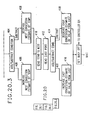
- FIGS. 20.1 - 20.3 when viewed as shown in FIG. 20 is a flowchart representation for the physical design machine system which illustrates how the controller and SPE array logically proceeds in determining the congestion estimate of a given net.
- the controller enters logic block 302 where the aforementioned NETID, Xmin, Xmax, Ymin, Ymax of the net is broadcast to all SPEs. The condition whether to add or subtract the nets congestion estimate values is also broadcast at this time.
- the process then proceeds to logic block 304 where the DMA jump address for a horizontal template process is initiated.
- the process then proceeds to logic block 306 where it resets the array and waits for a while. This reset signal initiates all SPEs' logic block 340, the function of which will be described shortly.
- the logic functions described at 304 and 306 actually initiates the array at the proper program.
- the waiting period in 306 is taken sufficiently large to insure the SPEs to have time to set the busy bit in the service word.
- the logic process then interrogates the service word until the busy bit of the service word becomes logical zero, as shown in 310 and 314. After that, the process enters the logic block 318 for broadcasting the jump address to all SPEs by DMA, for the horizontal modification process.
- the process then resets the array and waits as indicated at 320. This reset signal initiates as shown by 322 to all SPEs to perform logic block 362 and on.
- the logic process then proceeds to logic block 324 to read the service word from all of the SPEs in the array until the busy bit becomes zero, as shown in logic blocks 324 and 328. After this, the process repeats an analogous sequence of steps to 304-328 for the vertical congestion estimate of the given net.
- the subprocesses 304, 306 and 310 refers to the template generation for the horizontal congestion.
- the subprocesses 318, 320 and 324 accomplishes this modification relative to the previously described minimum rectangle.
- the SPEs are in a wait mode as indicated at 338, until it is reset by the controller by the action of reset logic block 306, which initiates logic block 340 to begin the horizontal template process.
- the process then proceeds to logic block 342 to set the busy bit of the service word to logical 1.
- the SPE then initializes the value of the variable TEMP to zero and sets the logical variable called LST-Neighbor to logical zero, 344.
- the actions of SPE now take on different courses depending on whether the L ST of the net is in the cell, the SPE is representing or not.
- the SPE marks its logical variable LST to be 1, and if the cell contains no LST, the variable LST is set to 0, as shown in logic blocks 348 and 350, respectively. Only the SPEs whose LST value is 1 now assigns TEMP value of 8 and sends to its neighbors appropriate values as shown in logic block 354. All SPEs, then repeat actions of 356, 358 and 360 or 332 and 334, until a further reset from the global controller at logic block 362. The logic process proceeds to logic block 356 to read from all neighbors, and then to logic block 358 where the question is asked, "Whether any value is received?".
- the process proceeds to logic block 366 to set the busy bit off, and proceeds to logic block 356 again.
- an SPE repeats attempting to receive from neighbors as long as no value is at each received failure of reception, it resets the busy bit to zero.
- the SPE sets the busy bit to one in logic block 332 and proceeds to perform actions of logic block 334.
- the process returns to the logic block 356 for a repeated attempt at receiving a value from a neighbor.
- the template is generated essentially by subprocesses 354, 356 and 334, until none of the SPEs is receiving any value from the neighbors as set forth at logic block 360.
- each SPE Upon reprompting from the controller at logic block 320, each SPE starts the modification process at logic block 362.
- the values just developed as the variable TEMP is intended for the congestion estimate of the West port of each cell.
- Logic block 374 modifies the value to zero if the cell is beyond the left boundary of the minimum rectangle as previously described, whereas logic block 380 sets it to 4 if the cell is next to the boundary LST.
- Logic block 384 sets it to 0 if the cell is above the minimum rectangle, logic block 390 sets it to 0 if the cell is below or to the right of the minimum rectangle.
- Logic blocks 400 and 402 set the value to either 4 or 0 depending upon whether the cell at the right side of boundary contains an LST or not, respectively.
- the logic block 398 marks the internal values, inside the minimum rectangle, to 1 if it was 0.
- the SPE process either adds in logic block 406 or subtracts in logic block 408, the TEMP value from the total West port congestion estimate.
- the same TEMP value is then transferred to the West neighbor for its use of the same TEMP value as the East port contribution from the given net, as shown in logic block 410.
- the process receives the value sent from its East neighbor 412, and either adds in logic block 416 or subtracts in logic block 418 the values just received from its East port congestion estimate.
- the logic process then proceeds to logic block 420 to set the busy bit to zero which marks the completion of the horizontal portion of the congestion estimate, and the SPEs await, as indicated at line 422, prompting for the symmetrical vertical process or some other process from the controller.
- the PORT COST of a cell boundary is developed according to the following theory, as a function of the channel capacity and the congestion estimate value of that port. These port costs when accumulated along a path together with the VIA COST, the cost of bending a wire on route, if any, constitute the cost of a wire route.
- the PORT COST, PC calculation takes the form as follows: if ⁇ C; excess supply case. CD + 0.5 C E + CE x 2 exp( ) for C > 3 if excess demand case, where 2 exp A denotes 2 to the power of A.
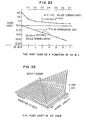
- FIG. 22 shows pictorially the PORT COST as a function of the CE and C whereas FIG. 23 presents another qualitative view of the PORT COST in the vertical axis as a function of the two variables.
- PORT COST Another term may be added to the PORT COST. This term might take the form of the direct distance cost, a fixed quantity for crossing a cell boundary everywhere, or might represent some measure of the internal cell complexity. This parameter is denoted as CD in the above equations.
- CD This parameter is denoted as CD in the above equations.
- the PORT COST calculation is done in every SPE in the array upon prompting by the controller. The exact flowchart of the process is straightforward and hence omitted.
- the via cost, VC, of a cell is calculated as a function of Vused, the number of vias already used in the cell.
- the function also makes use of the cell specific parameters, Vmax and Vmin, explained earlier.
- Each cell, or the corresponding SPE calculates the via cost when prompted by the controller as follows.
- wire net I is set forth in detail below. At the outset, the following values are developed in each SPE.
- the SPE contains in its memory, the following values, corresponding to the cell, or global constants stored earlier, including others.
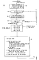
- F IG . 24 is a more detailed flowchart of logic block 268, wire-net-I, depicting the global routing process of FIG. 13.
- the source refers to that part of the net that is connected already in the process.
- one of the LSTs of the net is selected to be the initial source as designated at 424.
- the net may have a portion already partially routed previous to the global wiring process, in which case, the entire partial net serves as a source.
- An arbitrary LST can be selected as the initial source. However, different schemes may be utilized in selecting the initial source to enhance the general wirability.
- the remaining LSTs of the net are considered the sinks.
- the logic process continues to logic block 426 to propagate PATH COST, and then to logic block 428 to determine if the propagation was successful. If it was not successful, there is an overflow exit at logic line 430 and if it was successful, the logic process proceeds to logic block 432 to determine which of the reached sink would be connected to the source. The logic process then proceeds to logic block 434 to initiate a back trace and update from the sink to the source. The logic process then proceeds to logic block 436 to append the total newly connected route to the source. The logic process then proceeds to logic block 438 to determine if all LSTs are connected. If no, the process loops back to the logic block 426. If all LSTs are connected, the logic exits to logic block 270 of FIG. 13.
- an additional LST is connected to the already connected portion of the net until all LSTs are connected.
- Logic blocks 426 through 434 determinethe least cost path from the entire source to any of the sink LSTs, and connects the LST through the path. The length of the path is controlled to be within a differential detour limits (DLIM) of the shortest reachable distance from the source to the sinks.
- DLIM differential detour limits
- the subprocess 274 set forth in FIG. 13 is used to handle the overflow situation.
- One way to handle this situation is to record the overflow and proceed to the next net as illustrated. Then at the end of the total global routing, another process for the overflow handling can be initiated.
- the subprocess 274 can be replaced with in-situ overflow handling subprocess, that may modify some of the previously routed nets and retry the current net routing.
- the controller initiates the passes through the subprocesses 426 - 436 of FIG. 24, normally one less time than the total number of LSTs in the net, to connect all the LSTs.
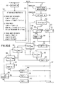
- FIG. 25 is the flowchart of the main subprocess 426 (propagate path costs) of FIG. 24 for the controller.
- the process starts at logic block 444 and proceeds to logic block 446 to first reset the array for propagation initialization. Then the process waits in the usual manner as shown by 448 and 450 until the busy bit is off. The logic process proceeds to logic block 452 to reset the array for propagation. The logic process then waits until the busy bit is off, in the usual manner. If the busy bit is off, the process proceeds to logic block 460 to determine if the End Flag is on. If the End Flag is on, the process exits to logic block 262 of the F IG. 13. If the End Flag is not on, the process then proceeds to logic block 464 to determine if the Action Flag is off. If the Action Flag is not off, the process returns to logic block 452. If the Action Flag is off, the logic process makes an overflow exit to logic block 274 of FIG. 13.
- FIGS. 26.1, 26.2 and 26.3 and 27 are the detail flowcharts of the propagate-path-costs subprocess 426 of FIG. 24, for the SPEs in the array.
- the SPEs are reset to propagation initialization, and the logic process proceeds to a logic block 474 where the busy bit is set on.
- Propagation initialization then takes place at logic block 476, with the pertinent variables and flags to be used in the propagation step being set forth in this logic block.
- all ports are cleared by reading all neighbors and ignoring the neighbor content, 476.1. This makes all ports ready to receive information from the neighbor by resetting the port mailbox flag mechanism.
- the valid indices are 0 through (D -1).
- the stack contains, for the given outgoing port, which of the incoming port contains the best cost path at the time indicated circularly by the stack pointer.
- the action counter, 476.2 is used to stop the SPE participation after the duration.
- the Action Flag bit, 476.3 is one of the service word bits used to indicate to the controller that the SPE is still within the duration of active propagation.
- the End Flag, 476.5 is another bit of the service word, which when set to logical 1 indicates to the controller that the cell (only the sink cells) with LST of net has received path costs from somewhere for the specified action period (D), i.e., all paths from the source to sink within the detour limit has been traversed.
- the Best Value for use of the sink cells is initialized to M, the number representing infinity.
- the controller prompts the propagation at logic block 452.
- Each prompting of the propagation lengthens the developing paths by one cell pitch.
- the controller checks if all SPEs finish this one cell propagation and further checks in logic block 460 to see if the End Flag is on.
- the End of Flag on signifies that all paths from source to sink within the detour limit have been traversed. If the End Flag is still not on, the controller checks, logic block 464, to see if any SPE is still within the active D propagation cycle and if so, prompts another propagation cycle, logic block 452, to the array. If, however, no SPE is in the active period an overflow is detected and appropriate action is taken, such as shown at logic block 274 of FIG. 13.
- Each pass through the propagation, 452 causes the array to process one additional length, in cell pitches, of the path.
- an SPE first checks whether the Action Counter value equals D, in logic block 486. If the Action Counter value is D, the logic process proceeds to logic 488 to clear all ports, and then to logic block 490 to set the Action Flag off. The logic process then proceeds to logic block 492 to set the busy bit to off and then proceed to wait as indicated at 494. If the Action Counter value is not D, the logic process proceeds in different courses depending on whether the SPE represents a source cell or not (logic block 496). Then the source cell SPEs proceeds to FIG.
- a path cost is 'sent' to a neighbor, it is meant that the actual sending of the value occurs only if the path cost is less than M, the value representing the infinity, as illustrated by logic blocks 506, 510 and 512. This applies in all cases when 'sending' a path cost to a neighbor as set forth below.
- the process proceeds from logic block 496 to logic block 520 of FIG. 26.2 to read all neighbors, i.e., path cost from N,E,S,W. If no value is sent from a neighbor the value is set to M. The logic process then proceeds to logic block 522 to determine whether any value other than M is received. If no finite value were received, the process proceeds to logic block 548 of FIG. 26.3. If any finite path cost was received the process proceeds to logic block 526 to set the Action Flag on and to increment the action counter. The logic process then branches at logic block 528 to either logic block 538, in case of sink cells, or to logic block 532, in case of intermediate cells.
- the SPEs representing the intermediate cells then compute bending path costs, as shown in logic block 532.
- the bending path cost is simply the sum of the via cost and the received path cost.
- the summary action represented by ⁇ (or ) in logic block 532 is set forth later.
- the logic then proceeds to logic block 534 where for each port, the following actions are taken:
- the logic process then proceeds from logic block 534 to logic block 548 on FIG. 26.3.
- the actions of sink cell SPEs branch from logic block 528 to logic block 538 where the value of the Action Counter is checked against D.
- the End Flag is set on at logic block 540 if the Action Counter equals D.
- the sink cell SPEs then proceed to logic block 542 to find the best incoming path cost and note the new best direction.
- the logic process then proceeds to logic block 544 where the new best value is compared against the best value stored earlier. If the earlier value is no worse, the process directly proceeds to logic block 548. If the new best value is better, the process proceeds to logic block 546 to update the best value, the best index, and the best port.
- the final action taken by the SPEs still active is to increment the stack pointer module D, as shown by logic blocks 548, 550 and 552. The process then sets the busy bit off and waits.
- Logic blocks 558, 560 and 562 are a more detailed version of logic block 532 where the values are added in logic block 558 and checked at logic block 560 to determine if the resultant value is greater than M. If the value is greater than M, it is set back to M at block 562. This modified addition is caused by the infinity representation conversion, for any number added to infinity results in infinity.
- the SPEs that represent the source cells basically pass appropriate port costs onto their neighbors as the path costs, for the duration of D number of passes.
- the Action Counter is incremented at each pass and when it reaches D, as set forth at logic block 486, the source SPE ceases to participate in the propagation and lowers the Action Flag.
- An intermediate cell basically waits until the first valid path cost has been sent to it from one or more of the neighbors to participate in the propagation.
- the SPEs representing the intermediate cells and the sink cells increment their stack pointers as set forth in logic block 548, at each pass. This variable is actually incremented in a circular fashion by the mechanism of logic blocks 548, 550 and 552.
- the non-source cells while they are active, by virtue of first having received a valid path cost from a neighbor, as set forth in logic blocks 520 and 522, sets the Action Flag, on, and increments the Action Counter.
- the Action Counter value is used to self-terminate, as set forth in logic block 486, the active period, as set forth in logic block 490, in the same manner it was set forth for the source cells. Any sink SPE raises the END flag, as set forth at logic block 540 to signal its termination of the active period which causes the end of the total propagation phase.
- the intermediate cells further process, as set forth in logic blocks 532 and 534, where first, the incoming path costs N,E,S,W, correspondingly from North, East, South, West ports are added to the via cost VC to develop NN, EE, SS and WW, the path cost of bending within the cell.
- the circled addition set forth in logic block 532 is carried out as shown in logic blocks 558, 560 and 562 as previously set forth. That is, if the values exceed M, which represent infinity, it is set back to M.
- the SPE determines the best incoming path direction and the cost, records the direction in the stack and sends the updated path cost to the neighbor. It is understood that by mention of sending the path cost to a neighbor, at all description, as set forth herein, it is meant that the path cost is sent only if it is less than the infinity, M, as shown in logic block 508. Taking the North port for example:
- a sink cell during the active period further performs the actions set forth in logic blocks 542, 544 and 546.
- the sink cell finds the best of incoming path costs, N,E,S,W and notes the winning direction as set forth in logic block 542. If the new best path cost is better than the old best value the Best Value, Best Port, Best Index are updated as shown in the subprocess as set forth in logic block 546.
- the total number of passes the controller prompts the array for propagation is DLIM plus the reachable distance between source and sink plus one.
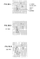
- FIGS. 28.1 - 28.8 illustrate an example of the steps taken in computing the propagation of path cost.
- the cells marked A are the source cells, depicted as a partial net.
- the cells B and C are two additional LST's of the net.
- the reachable distance from the source to sink is four cell pitches, connecting A to C.
- the numbers in the cell represent the cell's action counter at the beginning of the passes.
- the SPE at C raises the END flag which effectively halts the path cost propagation process.
- ORing bus structure illustrated in FIG. 3, from array to the controller via the array I/O processor, is gainfully employed in controller- array communications.
- service word ORed from all SPEs to the array enables the controller to recognize the following:
- the controller initiates the subprocess set forth in logic block 432 which determines which of the reached sink cells (in case more than one are reached at the time of the halt, e.g., both D and C are reached as set forth in FIGS. 28.1 - 28.8) is to be connected to the source.
- the candidate sink cell to be connected to the source which is the partially connected portion of the net so far into the net routing, is the sink that contains the best of the BEST VALUE
- the sink cells whose Action Flag is ON all participate in this phase and the controller, by polling them, determines which of these would be the candidate. This is accomplished by the sink SPEs which have been reached (whose action flag is ON) raising their XY response lines, and then the controller selecting the responding rows and columns one at a time and interrogating their best values to find the minimum. Once the candidate sink is thus determined the controller . informs the chosen SPE of its status.
- the controller prompts the array, initializes appropriate flags and informs the candidate sink via the I/O register communications (i.e., the flag mechanism of the AIN latch), to initialize the back-trace.
- FIGS. 29.1 and 29.2 when viewed with FIG. 29.1 on the top and FIG. 29.2 on the bottom is a flow chart indicative of the respective SPE programs in the array.
- the controller terminates the back-trace process when it detects the END flag going up.
- the END flag a designated bit in the service word is initially down and is used by the source cell SPEs to signal the end of the back-trace.
- the actions of the controller for the back-trace routine is straightforward and the detail flowchart is not shown.
- the manner by which the cells record as being part of the net is through the use of the EXIT mask associated to the net ID.
- the EXIT mask is a four bit variable where each bit represents the corresponding directions N,E,S,W, respectively.
- the EXIT mask associated to a net signifies that the net passes through the cell, and is connected through the ports that correspond to the bits set as 1 in the EXIT mask.
- the SPEs when prompted by the controller, first reset the END FLAG to zero and clear all ports at logic block 568.
- the SPEs then perform specialized actions depending upon the cell a given SPE represents. This is determined at logic block 570 relative to cell status: a source, a sink, or an intermediate cell.
- the sink cell SPE then proceeds to determine if the cell is a candidate sink. This is accomplished by reading the service word as indicated at logic block 572 until the AIN flag bit becomes 1. Once the AIN bit is read as ON, the process in the candidate sink SPE proceeds to logic block 576.
- the controller sets the AIN flag bit of the candidate sink by uniquely selecting the cell and sending an arbitrary word to the cell I-register, which sets the AIN flag as previously set forth relative to the SPE block diagram.
- the SPE of the candidate sink cell then initiates the back-trace by first copying the Best Direction into the direction to back-trace (DIRC) and Best Index into the stack pointer as shown at logic block 576.
- the back-trace outgoing ports channel capacity is decremented to indicate the usage of a track by the net, as set forth at logic block 578.
- the nets EXIT mask is modified by setting the bit corresponding to the DIRC, as indicated at logic block 580, stack pointer decremented, in a circular manner (i.e., if -1, reset to D -1) as indicated at logic block 582, and finally, the stack pointer is sent to the neighbor indicated by the DIRC, as set forth at logic block 584.
- the intermediate SPEs read all their neighbors 'as indicated at logic block 588 until some valid data is passed to them. If a value is received, which is a stack pointer value, it notes the incoming direction as INPORT, as set forth at logic block 592, and assigns the value received as its stack pointer as indicated at logic block 594, and it decrements the INPORT channel capacity as set forth at logic block 596.
- the outgoing direction for the back-trace is determined as set forth at logic block 598, by looking up the stored direction in the INPORTs flag stack pointed to by the stack pointer, and then the proceeds to perform the logic blocks 578 through 584 as previously set forth.
- the EXIT mask is marked as set forth at logic block 580, the INPORT bit as well as the DIRC port bit, are set to 1.
- a source cell For a source cell, all neighbors are read as indicated at logic block 602 until a value is received. If a value is received, the process proceeds to logic block 606 to note the port where the value came in as the INPORT.
- the source cell which receives the value from its neighbor, then updates the channel capacity of the INPORT as indicated at logic block 608, and marks the net exit mask as indicated at logic block 610 and raises the END FLAG at logic block 610.
- processor array is at least as large as the chip in question, in its horizontal and vertical cell dimensions.
- the processor array must be a reasonable size to be practical, it is possible in principle to utilize a small array to emulate without much penalty, a machine representing chips of a size much greater than the given machine. Regardless of the size of the array, it is natural that problem chips of bigger size than the machine would be put to task.
- the mechanism described here provides a novel solution to this end.
- M and N the number of cells of the chip in horizontal dimension and vertical dimension, respectively. Further, denote by m and n the number of columns and rows, respectively, of the processor array of SPEs of FIG. 2.
- the chip is to be partitioned, conceptually, into FRAMES that are the same as the machine size, N rows by M columns of cells.
- the machine array boundaries as shown in the FIG. 2 correspond with the boundaries of the FRAME of cells in the chip.
- the end around connections of the neighborhood at the boundary cells make possible the communication between adjacent cells at the frame boundaries on the chip.
- Each SPE of the machine represents, not just one cell of the chip, but up to (Q + 1) x (S + 1) cells regularly spaced over the entire chip.
- the end around neighbor connection of the array is not strictly necessary to implement the FRAME concept.
- the FRAMES can be thought of as folded in accordion style in both dimensions.
- One disadvantage of folding in such manner is that the cell indices in alternating frames are reversed, thereby necessitating an extensive programming overhead to account for these direction reversals.
- Yet another disadvantage is that on a one direction sweep operation, pipelining of many frame's worth of sweeping is not possible under this arrangement.
- the chip is considered to be superimposed on the array of frames each of which is identical in size to the machine processor array.
- the chip is lined up against the left and bottom edges of these frame arrays which is the origin of the X and Y coordinates.
- Each frame has a frame ID, called FID that is in the range of
- the horizontal and vertical cell coordinates relative to a frame are called FXID and FYID, respectively.
- the translation of chip cells XID and YID to the frame relative values are developed by: where denotes the quotient and x mod y denotes the remainder, respectively, of x determined by the relation, FIG. 30 depicts the chip frame, frame ID, FXID, FYID, XID and YID of the cells.
- Each SPE of the machine allocates its local memory, 196 of FIG. 6, into common area and the rest that are equally partitioned to each frame of the chip. All common data such as the aforementioned detour limit, stack pointer, current net ID, etc., and the SPE program reside in this common area. All cell specific .data, such as the cell ID's, congestion estimates, the net data, the port costs, via-related values, etc. are then stored in the corresponding frame area of the memory. Accordingly, the overall memory requirement of the whole machine would be almost the same as the large machine of the same size as the chip, even though the number of processors are smaller. Each SPE simply requires more memory space to hold data for all the cells it represents.
- the controller as well as neighbors must specify what frame's data is being sent to the SPE at the time of the data transfers, unless the data is of framewise common nature. Also, whenever the data is received by an SPE, it stores the data in the proper partition of the memory corresponding to the accompanying frame number it received with the data.
- the controller To actually communicate to a cell, the controller must first convert the cell ID (XID, YID) into the frame relevant parameters (FID, FXID, FYID) and select FXID, FYID on the horizontal and vertical selectors, respectively, before the transmission of data and frame number FID to the SPE.
- the frame number accompanying the data would be the same if the neighbor is in the same frame as the cell.
- FIG. 31 illustrates a flowchart of the paradigm for the full size machine.
- the left end cell computes as indicated at logic block 616, with the results passed to its East neighbor as shown in logic block 618.
- the middle cells receive information from the West as indicated at logic block 620, with computations being based on this information being performed at logic block 622.
- the results of the computations at logic block 622 is passed to its East neighbor as shown in logic block 618.
- the right end cells receive information from the West neighbor as indicated at logic block 624, with computations being performed on this information as indicated at logic block 626. At the completion of the computation the controller is notified as indicated in logic block 628.
- FIGS. 32.1 - 32.3 illustrate the concept in timed steps.
- the machine SPE's busy status and the corresponding cells on the chip is shaded.
- the frame is shown in bold lines for reference.
- the total sweep time for the full size machine is M, and the framed machine is M X , asymptotically. It is evident that the performance penalty for this type of operation is not very much.
- the SPE resets the busy flag only after it processed all tasks in the work stack. It is then natural that, at any given time, each SPE may be processing the propagation of a cell in different frames.
- the performance penalty when the machine size is small (say less than 8 x 8) is quite high. The penalty progressively lessens as the machine size increases towards the chip size. Compared to an infinite chip with infinite machine, a 32 x 32 processor array machine would incur a doubling of the processing time, on the average. A detailed analysis of this performance penalty appears elsewhere.
- the 5 x 5 machine would incur over 3 times the penalty for connecting the example case, insofar as the computation time in the SPE is essentially spent in performing the logic functions of the logic blocks 532 and 534 of FIG. 26.2 for the propagation of path costs in logic block 426 of FIG. 24.
- FIG. 34 illustrates the paradigm from an SPE's viewpoint.
- the center cell SPE proceeds to compute its task and send the results of the computation to the 4 neighbors, as shown in 634 and 636.
- the SPEs representing other cells along the center row or the column of the chip (yes branch off 640), waits until a value is received from the center direction (642 and 644), computes on the received value (646), results of which then are sent to all 3 of its outward neighbors.
- the other SPEs, representing cells not in the center row or column waits until both of its inward neighbors have sent data (652, 654), and proceeds to compute on the received data (656), the results of which are sent to both of its outward neighbors (658).
- the processing activity propagates out from the center in a diamond-like wave until the 4 corners are reached.
- the processing progresses in somewhat irregular shape outward as shown in FIGS. 35 and 36.
- the performance time penalty is much less than the ratio of sizes; chip vs. machine, given that the machine size is reasonable.
- FIGS. 35 and 36 illustrates how the order of processing the work stack can be influenced by some predetermined criteria.
- Each SPE in this example processed the cell closer to the center of the chip first.
Landscapes
- Engineering & Computer Science (AREA)
- Theoretical Computer Science (AREA)
- Computer Hardware Design (AREA)
- Physics & Mathematics (AREA)
- General Engineering & Computer Science (AREA)
- Geometry (AREA)
- Evolutionary Computation (AREA)
- General Physics & Mathematics (AREA)
- Computer Networks & Wireless Communication (AREA)
- Design And Manufacture Of Integrated Circuits (AREA)
- Multi Processors (AREA)
- Semiconductor Integrated Circuits (AREA)
- Internal Circuitry In Semiconductor Integrated Circuit Devices (AREA)
Applications Claiming Priority (2)
| Application Number | Priority Date | Filing Date | Title |
|---|---|---|---|
| US272880 | 1981-06-12 | ||
| US06/272,880 US4484292A (en) | 1981-06-12 | 1981-06-12 | High speed machine for the physical design of very large scale integrated circuits |
Publications (3)
| Publication Number | Publication Date |
|---|---|
| EP0067304A2 true EP0067304A2 (de) | 1982-12-22 |
| EP0067304A3 EP0067304A3 (en) | 1984-07-25 |
| EP0067304B1 EP0067304B1 (de) | 1989-02-01 |
Family
ID=23041675
Family Applications (1)
| Application Number | Title | Priority Date | Filing Date |
|---|---|---|---|
| EP82103941A Expired EP0067304B1 (de) | 1981-06-12 | 1982-05-06 | Verarbeitungsnetz und Verfahren zur physischen Planung von in sehr hohem Grad integrierten Schaltkreisen |
Country Status (5)
| Country | Link |
|---|---|
| US (1) | US4484292A (de) |
| EP (1) | EP0067304B1 (de) |
| JP (2) | JPS58153A (de) |
| CA (1) | CA1166759A (de) |
| DE (1) | DE3279427D1 (de) |
Cited By (2)
| Publication number | Priority date | Publication date | Assignee | Title |
|---|---|---|---|---|
| EP0346630A3 (de) * | 1988-06-10 | 1991-06-12 | International Business Machines Corporation | Globale Verdrahtung durch Wegnahme von redundanten Wegen |
| US20220366118A1 (en) * | 2020-09-21 | 2022-11-17 | Taiwan Semiconductor Manufacturing Co., Ltd. | Method for optimizing floor plan for an integrated circuit |
Families Citing this family (98)
| Publication number | Priority date | Publication date | Assignee | Title |
|---|---|---|---|---|
| US4484292A (en) * | 1981-06-12 | 1984-11-20 | International Business Machines Corporation | High speed machine for the physical design of very large scale integrated circuits |
| JPH077825B2 (ja) * | 1981-08-13 | 1995-01-30 | 富士通株式会社 | ゲートアレイの製造方法 |
| JPS58190036A (ja) * | 1982-04-23 | 1983-11-05 | Fujitsu Ltd | ゲ−ト・アレイ大規模集積回路装置 |
| JPS5961944A (ja) * | 1982-09-30 | 1984-04-09 | Fujitsu Ltd | マスタスライス集積回路の製造方法 |
| US4584653A (en) * | 1983-03-22 | 1986-04-22 | Fujitsu Limited | Method for manufacturing a gate array integrated circuit device |
| US4580228A (en) * | 1983-06-06 | 1986-04-01 | The United States Of America As Represented By The Secretary Of The Army | Automated design program for LSI and VLSI circuits |
| US4612618A (en) * | 1983-06-10 | 1986-09-16 | Rca Corporation | Hierarchical, computerized design of integrated circuits |
| US4593363A (en) * | 1983-08-12 | 1986-06-03 | International Business Machines Corporation | Simultaneous placement and wiring for VLSI chips |
| NL8303536A (nl) * | 1983-10-14 | 1985-05-01 | Philips Nv | Geintegreerde schakeling op grote schaal welke verdeeld is in isochrone gebieden, werkwijze voor het machinaal ontwerpen van zo een geintegreerde schakeling, en werkwijze voor het machinaal testen van zo een geintegreerde schakeling. |
| GB8328909D0 (en) * | 1983-10-28 | 1983-11-30 | Hutton G H | Manufacturing pattern-bearing article |
| JPS6124250A (ja) * | 1984-07-13 | 1986-02-01 | Nippon Gakki Seizo Kk | 半導体集積回路装置 |
| US5226171A (en) * | 1984-12-03 | 1993-07-06 | Cray Research, Inc. | Parallel vector processing system for individual and broadcast distribution of operands and control information |
| JPS61199166A (ja) * | 1985-03-01 | 1986-09-03 | Nec Corp | 配線経路探索装置 |
| US4701860A (en) * | 1985-03-07 | 1987-10-20 | Harris Corporation | Integrated circuit architecture formed of parametric macro-cells |
| JPS63278249A (ja) * | 1986-12-26 | 1988-11-15 | Toshiba Corp | 半導体集積回路装置の配線方法 |
| US4965739A (en) * | 1987-03-26 | 1990-10-23 | Vlsi Technology, Inc. | Machine process for routing interconnections from one module to another module and for positioning said two modules after said modules are interconnected |
| US4768154A (en) * | 1987-05-08 | 1988-08-30 | Telesis Systems Corporation | Computer aided printed circuit board wiring |
| US5182719A (en) * | 1988-06-09 | 1993-01-26 | Hitachi, Ltd. | Method of fabricating a second semiconductor integrated circuit device from a first semiconductor integrated circuit device |
| US5003487A (en) * | 1988-06-28 | 1991-03-26 | International Business Machines Corporation | Method and apparatus for performing timing correction transformations on a technology-independent logic model during logic synthesis |
| US5187784A (en) * | 1989-01-13 | 1993-02-16 | Vlsi Technology, Inc. | Integrated circuit placement method using netlist and predetermined ordering constraints to produce a human readable integrated circuit schematic diagram |
| JP2509755B2 (ja) * | 1990-11-22 | 1996-06-26 | 株式会社東芝 | 半導体集積回路製造方法 |
| JP3033203B2 (ja) * | 1991-01-25 | 2000-04-17 | 株式会社日立製作所 | 配線経路探索装置及び配線経路探索方法 |
| US5339253A (en) * | 1991-06-14 | 1994-08-16 | International Business Machines Corporation | Method and apparatus for making a skew-controlled signal distribution network |
| JP3172211B2 (ja) * | 1991-09-05 | 2001-06-04 | 富士通株式会社 | 回路合成システム |
| US5341310A (en) * | 1991-12-17 | 1994-08-23 | International Business Machines Corporation | Wiring layout design method and system for integrated circuits |
| JPH06196563A (ja) * | 1992-09-29 | 1994-07-15 | Internatl Business Mach Corp <Ibm> | Vlsiの配線設計に対するコンピュータ実施可能な過密領域配線方法 |
| CA2102855A1 (en) * | 1992-12-29 | 1994-06-30 | Albon E. Gilbert | Jumper cable selection and routing system |
| CN1058110C (zh) * | 1993-06-21 | 2000-11-01 | 松下电子工业株式会社 | 半导体集成电路的布图设计方法 |
| US5533148A (en) * | 1993-09-30 | 1996-07-02 | International Business Machines Corporation | Method for restructuring physical design images into hierarchical data models |
| US5818726A (en) * | 1994-04-18 | 1998-10-06 | Cadence Design Systems, Inc. | System and method for determining acceptable logic cell locations and generating a legal location structure |
| US5495419A (en) * | 1994-04-19 | 1996-02-27 | Lsi Logic Corporation | Integrated circuit physical design automation system utilizing optimization process decomposition and parallel processing |
| US5914887A (en) * | 1994-04-19 | 1999-06-22 | Lsi Logic Corporation | Congestion based cost factor computing apparatus for integrated circuit physical design automation system |
| US6155725A (en) * | 1994-04-19 | 2000-12-05 | Lsi Logic Corporation | Cell placement representation and transposition for integrated circuit physical design automation system |
| US5815403A (en) * | 1994-04-19 | 1998-09-29 | Lsi Logic Corporation | Fail-safe distributive processing method for producing a highest fitness cell placement for an integrated circuit chip |
| US5557533A (en) * | 1994-04-19 | 1996-09-17 | Lsi Logic Corporation | Cell placement alteration apparatus for integrated circuit chip physical design automation system |
| US6493658B1 (en) | 1994-04-19 | 2002-12-10 | Lsi Logic Corporation | Optimization processing for integrated circuit physical design automation system using optimally switched fitness improvement algorithms |
| US5875117A (en) * | 1994-04-19 | 1999-02-23 | Lsi Logic Corporation | Simultaneous placement and routing (SPAR) method for integrated circuit physical design automation system |
| US5963975A (en) * | 1994-04-19 | 1999-10-05 | Lsi Logic Corporation | Single chip integrated circuit distributed shared memory (DSM) and communications nodes |
| US5636129A (en) * | 1994-04-20 | 1997-06-03 | Her; One-Hsiow A. | Electrical routing through fixed sized module and variable sized channel grids |
| US5638288A (en) * | 1994-08-24 | 1997-06-10 | Lsi Logic Corporation | Separable cells having wiring channels for routing signals between surrounding cells |
| US5587923A (en) * | 1994-09-07 | 1996-12-24 | Lsi Logic Corporation | Method for estimating routability and congestion in a cell placement for integrated circuit chip |
| US5615127A (en) * | 1994-11-30 | 1997-03-25 | International Business Machines Corporation | Parallel execution of a complex task partitioned into a plurality of entities |
| US5798541A (en) * | 1994-12-02 | 1998-08-25 | Intel Corporation | Standard semiconductor cell with contoured cell boundary to increase device density |
| US5768146A (en) * | 1995-03-28 | 1998-06-16 | Intel Corporation | Method of cell contouring to increase device density |
| US6308143B1 (en) * | 1996-02-21 | 2001-10-23 | Matsushita Electric Industrial Co., Ltd. | Layout input apparatus, layout input method, layout verification apparatus, and layout verification method |
| US6226560B1 (en) * | 1996-03-04 | 2001-05-01 | International Business Machines Corporation | Method and apparatus for optimizing the path of a physical wire |
| US5812740A (en) * | 1996-06-28 | 1998-09-22 | Lsi Logic Corporation | Advanced modular cell placement system with neighborhood system driven optimization |
| US5831863A (en) * | 1996-06-28 | 1998-11-03 | Lsi Logic Corporation | Advanced modular cell placement system with wire length driven affinity system |
| US5870312A (en) * | 1996-06-28 | 1999-02-09 | Lsi Logic Corporation | Advanced modular cell placement system with dispersion-driven levelizing system |
| US5963455A (en) * | 1996-06-28 | 1999-10-05 | Lsi Logic Corporation | Advanced modular cell placement system with functional sieve optimization technique |
| US6030110A (en) * | 1996-06-28 | 2000-02-29 | Lsi Logic Corporation | Advanced modular cell placement system with median control and increase in resolution |
| US5844811A (en) * | 1996-06-28 | 1998-12-01 | Lsi Logic Corporation | Advanced modular cell placement system with universal affinity driven discrete placement optimization |
| US6026223A (en) * | 1996-06-28 | 2000-02-15 | Scepanovic; Ranko | Advanced modular cell placement system with overlap remover with minimal noise |
| US5872718A (en) * | 1996-06-28 | 1999-02-16 | Lsi Logic Corporation | Advanced modular cell placement system |
| US5835381A (en) * | 1996-06-28 | 1998-11-10 | Lsi Logic Corporation | Advanced modular cell placement system with minimizing maximal cut driven affinity system |
| US5867398A (en) * | 1996-06-28 | 1999-02-02 | Lsi Logic Corporation | Advanced modular cell placement system with density driven capacity penalty system |
| US5808899A (en) * | 1996-06-28 | 1998-09-15 | Lsi Logic Corporation | Advanced modular cell placement system with cell placement crystallization |
| US6067409A (en) * | 1996-06-28 | 2000-05-23 | Lsi Logic Corporation | Advanced modular cell placement system |
| US5914888A (en) * | 1996-06-28 | 1999-06-22 | Lsi Logic Corporation | Advanced modular cell placement system with coarse overflow remover |
| US5892688A (en) * | 1996-06-28 | 1999-04-06 | Lsi Logic Corporation | Advanced modular cell placement system with iterative one dimensional preplacement optimization |
| US6085032A (en) * | 1996-06-28 | 2000-07-04 | Lsi Logic Corporation | Advanced modular cell placement system with sinusoidal optimization |
| US5870311A (en) * | 1996-06-28 | 1999-02-09 | Lsi Logic Corporation | Advanced modular cell placement system with fast procedure for finding a levelizing cut point |
| US5959993A (en) * | 1996-09-13 | 1999-09-28 | Lsi Logic Corporation | Scheduler design for ATM switches, and its implementation in a distributed shared memory architecture |
| US5831980A (en) * | 1996-09-13 | 1998-11-03 | Lsi Logic Corporation | Shared memory fabric architecture for very high speed ATM switches |
| US5980093A (en) * | 1996-12-04 | 1999-11-09 | Lsi Logic Corporation | Integrated circuit layout routing using multiprocessing |
| US5818730A (en) | 1996-12-05 | 1998-10-06 | Xilinx, Inc. | FPGA one turn routing structure and method using minimum diffusion area |
| US6031981A (en) * | 1996-12-19 | 2000-02-29 | Cirrus Logic, Inc. | Reconfigurable gate array cells for automatic engineering change order |
| US5828230A (en) * | 1997-01-09 | 1998-10-27 | Xilinx, Inc. | FPGA two turn routing structure with lane changing and minimum diffusion area |
| US6074429A (en) * | 1997-03-03 | 2000-06-13 | Motorola, Inc. | Optimizing combinational circuit layout through iterative restructuring |
| US6266802B1 (en) * | 1997-10-27 | 2001-07-24 | International Business Machines Corporation | Detailed grid point layout using a massively parallel logic including an emulator/simulator paradigm |
| US6230304B1 (en) | 1997-12-24 | 2001-05-08 | Magma Design Automation, Inc. | Method of designing a constraint-driven integrated circuit layout |
| US6077309A (en) * | 1998-01-07 | 2000-06-20 | Mentor Graphics Corporation | Method and apparatus for locating coordinated starting points for routing a differential pair of traces |
| JP3184796B2 (ja) * | 1998-03-19 | 2001-07-09 | インターナショナル・ビジネス・マシーンズ・コーポレ−ション | 配線設計装置およびその方法 |
| GB2337346B (en) * | 1998-05-15 | 2001-04-11 | Lsi Logic Corp | Integrated circuit routing |
| US6192508B1 (en) * | 1998-06-12 | 2001-02-20 | Monterey Design Systems | Method for logic optimization for improving timing and congestion during placement in integrated circuit design |
| US6263480B1 (en) * | 1998-12-30 | 2001-07-17 | International Business Machines Corporation | Efficient tracing of shorts in very large nets in hierarchical designs |
| US6519751B2 (en) * | 2000-03-31 | 2003-02-11 | Intel Corporation | Method and apparatus for accurate crosspoint allocation in VLSI area routing |
| US6415426B1 (en) | 2000-06-02 | 2002-07-02 | Incentia Design Systems, Inc. | Dynamic weighting and/or target zone analysis in timing driven placement of cells of an integrated circuit design |
| US6775808B1 (en) * | 2000-08-03 | 2004-08-10 | Monterey Design Systems, Inc. | Method and apparatus for generating sign-off prototypes for the design and fabrication of integrated circuits |
| US6763512B2 (en) * | 2001-04-06 | 2004-07-13 | Sun Microsystems, Inc. | Detailed method for routing connections using tile expansion techniques and associated methods for designing and manufacturing VLSI circuits |
| JP4429593B2 (ja) * | 2002-11-22 | 2010-03-10 | パナソニック株式会社 | 半導体装置のレイアウト検証方法 |
| US7415644B2 (en) * | 2004-10-22 | 2008-08-19 | International Business Machines Corporation | Self-repairing of microprocessor array structures |
| US8300798B1 (en) | 2006-04-03 | 2012-10-30 | Wai Wu | Intelligent communication routing system and method |
| US8045546B1 (en) * | 2008-07-08 | 2011-10-25 | Tilera Corporation | Configuring routing in mesh networks |
| JP5145167B2 (ja) * | 2008-08-20 | 2013-02-13 | ルネサスエレクトロニクス株式会社 | クロックドメインチェック方法及びクロックドメインチェック用プログラム並びに記録媒体 |
| US7971174B1 (en) * | 2008-09-18 | 2011-06-28 | Cadence Design Systems, Inc. | Congestion aware pin optimizer |
| US8464196B1 (en) * | 2012-03-28 | 2013-06-11 | Cadence Design Systems, Inc. | Method and system for routing optimally between terminals through intermediate vias in a circuit design |
| US9003349B1 (en) | 2013-06-28 | 2015-04-07 | Cadence Design Systems, Inc. | Methods, systems, and articles of manufacture for implementing a physical electronic design with area-bounded tracks |
| US8984465B1 (en) | 2013-06-28 | 2015-03-17 | Cadence Design Systems, Inc. | Methods, systems, and articles of manufacture for automatically assigning track patterns to regions for physical implementation of an electronic design |
| US9117052B1 (en) | 2012-04-12 | 2015-08-25 | Cadence Design Systems, Inc. | Methods, systems, and articles of manufacture for interactively implementing physical electronic designs with track patterns |
| US9251299B1 (en) | 2013-06-28 | 2016-02-02 | Cadence Design Systems, Inc. | Methods, systems, and articles of manufacture for associating track patterns with rules for electronic designs |
| US8935649B1 (en) | 2012-08-31 | 2015-01-13 | Cadence Design Systems, Inc. | Methods, systems, and articles of manufacture for routing an electronic design using spacetiles |
| US9075932B1 (en) | 2012-08-31 | 2015-07-07 | Candence Design Systems, Inc. | Methods and systems for routing an electronic design using spacetiles |
| US9213793B1 (en) | 2012-08-31 | 2015-12-15 | Cadence Design Systems, Inc. | Methods, systems, and articles of manufacture for implementing electronic designs using flexible routing tracks |
| US9183343B1 (en) * | 2012-08-31 | 2015-11-10 | Cadence Design Systems, Inc. | Methods, systems, and articles of manufacture for implementing high current carrying interconnects in electronic designs |
| US9104830B1 (en) | 2013-06-28 | 2015-08-11 | Cadence Design Systems, Inc. | Methods, systems, and articles of manufacture for assigning track patterns to regions of an electronic design |
| US9817941B2 (en) | 2012-12-04 | 2017-11-14 | Cadence Design Systems, Inc. | Methods, systems, and articles of manufacture for implementing high current carrying interconnects in electronic designs |
| US9165103B1 (en) | 2013-06-28 | 2015-10-20 | Cadence Design Systems, Inc. | Methods, systems, and articles of manufacture for tessellating and labeling routing space for routing electronic designs |
Family Cites Families (8)
| Publication number | Priority date | Publication date | Assignee | Title |
|---|---|---|---|---|
| US3653072A (en) * | 1970-01-08 | 1972-03-28 | Texas Instruments Inc | Process for producing circuit artwork utilizing a data processing machine |
| US3684871A (en) * | 1970-10-30 | 1972-08-15 | Systonetics Inc | Network plotting system |
| US3979728A (en) * | 1973-04-13 | 1976-09-07 | International Computers Limited | Array processors |
| DE2445368A1 (de) * | 1974-09-23 | 1976-04-01 | Siemens Ag | Verfahren zur herstellung fuer maskenvorlagen fuer integrierte halbleiterschaltungen |
| US4065808A (en) * | 1975-01-25 | 1977-12-27 | U.S. Philips Corporation | Network computer system |
| JPS5842621B2 (ja) * | 1976-10-18 | 1983-09-21 | 日本電信電話株式会社 | 配線径路決定装置 |
| JPS5846173B2 (ja) * | 1980-09-22 | 1983-10-14 | 日本電信電話株式会社 | 論理配線設計方式 |
| US4484292A (en) * | 1981-06-12 | 1984-11-20 | International Business Machines Corporation | High speed machine for the physical design of very large scale integrated circuits |
-
1981
- 1981-06-12 US US06/272,880 patent/US4484292A/en not_active Expired - Lifetime
-
1982
- 1982-04-07 CA CA000400638A patent/CA1166759A/en not_active Expired
- 1982-05-06 EP EP82103941A patent/EP0067304B1/de not_active Expired
- 1982-05-06 DE DE8282103941T patent/DE3279427D1/de not_active Expired
- 1982-06-10 JP JP57098632A patent/JPS58153A/ja active Granted
- 1982-08-03 JP JP57134834A patent/JPS5875265A/ja active Granted
Cited By (4)
| Publication number | Priority date | Publication date | Assignee | Title |
|---|---|---|---|---|
| EP0346630A3 (de) * | 1988-06-10 | 1991-06-12 | International Business Machines Corporation | Globale Verdrahtung durch Wegnahme von redundanten Wegen |
| US20220366118A1 (en) * | 2020-09-21 | 2022-11-17 | Taiwan Semiconductor Manufacturing Co., Ltd. | Method for optimizing floor plan for an integrated circuit |
| US11853675B2 (en) | 2020-09-21 | 2023-12-26 | Taiwan Semiconductor Manufacturing Co., Ltd. | Method for optimizing floor plan for an integrated circuit |
| US11893334B2 (en) * | 2020-09-21 | 2024-02-06 | Taiwan Semiconductor Manufacturing Co., Ltd. | Method for optimizing floor plan for an integrated circuit |
Also Published As
| Publication number | Publication date |
|---|---|
| CA1166759A (en) | 1984-05-01 |
| JPS5875265A (ja) | 1983-05-06 |
| DE3279427D1 (en) | 1989-03-09 |
| JPS58153A (ja) | 1983-01-05 |
| EP0067304A3 (en) | 1984-07-25 |
| JPH0236068B2 (de) | 1990-08-15 |
| US4484292A (en) | 1984-11-20 |
| JPH0236067B2 (de) | 1990-08-15 |
| EP0067304B1 (de) | 1989-02-01 |
Similar Documents
| Publication | Publication Date | Title |
|---|---|---|
| EP0067304B1 (de) | Verarbeitungsnetz und Verfahren zur physischen Planung von in sehr hohem Grad integrierten Schaltkreisen | |
| US4593351A (en) | High speed machine for the physical design of very large scale integrated circuits | |
| US6286128B1 (en) | Method for design optimization using logical and physical information | |
| US5535408A (en) | Processor chip for parallel processing system | |
| US5757656A (en) | Method for routing breakouts | |
| US4577276A (en) | Placement of components on circuit substrates | |
| EP0132926B1 (de) | Parallel-Prozessor | |
| US4593363A (en) | Simultaneous placement and wiring for VLSI chips | |
| US4709327A (en) | Parallel processor/memory circuit | |
| US5146608A (en) | Parallel processor array system controlled in response to composition status signal | |
| Heyns et al. | A line-expansion algorithm for the general routing problem with a guaranteed solution | |
| Cho et al. | Four-bend top-down global routing | |
| Olukotun et al. | A preliminary investigation into parallel routing on a hypercube computer | |
| Krohn | An over-cell gate array channel router | |
| Markov et al. | Optimization techniques for two-dimensional placement | |
| US6615401B1 (en) | Blocked net buffer insertion | |
| JP3208014B2 (ja) | 配線経路調査装置および配線経路調査方法 | |
| JP2523702B2 (ja) | 半導体集積回路の自動配線方法 | |
| JPS5846173B2 (ja) | 論理配線設計方式 | |
| JP2751199B2 (ja) | 配線経路探索方式及び装置 | |
| Goto et al. | lambda, an integrated master-slice LSI CAD system | |
| Matsuda et al. | LAMBDA: A Quick, Low Cost Layout Design System for Master-Slice LSIs | |
| Alia et al. | Automated module placement and wire routeing according to a structured biplanar scheme in printed boards | |
| Tzionas et al. | New algorithm for three-dimensional minimum cost path planning and its VLSI implementation by means of a three-dimensional cellular automata architecture | |
| Diessel et al. | Ordered partial task compaction on mesh connected computers |
Legal Events
| Date | Code | Title | Description |
|---|---|---|---|
| PUAI | Public reference made under article 153(3) epc to a published international application that has entered the european phase |
Free format text: ORIGINAL CODE: 0009012 |
|
| AK | Designated contracting states |
Designated state(s): BE DE FR GB IT |
|
| 17P | Request for examination filed |
Effective date: 19830420 |
|
| PUAL | Search report despatched |
Free format text: ORIGINAL CODE: 0009013 |
|
| AK | Designated contracting states |
Designated state(s): BE DE FR GB IT |
|
| 17Q | First examination report despatched |
Effective date: 19860117 |
|
| GRAA | (expected) grant |
Free format text: ORIGINAL CODE: 0009210 |
|
| AK | Designated contracting states |
Kind code of ref document: B1 Designated state(s): BE DE FR GB IT |
|
| PG25 | Lapsed in a contracting state [announced via postgrant information from national office to epo] |
Ref country code: BE Effective date: 19890201 |
|
| REF | Corresponds to: |
Ref document number: 3279427 Country of ref document: DE Date of ref document: 19890309 |
|
| ITF | It: translation for a ep patent filed | ||
| ET | Fr: translation filed | ||
| PLBE | No opposition filed within time limit |
Free format text: ORIGINAL CODE: 0009261 |
|
| STAA | Information on the status of an ep patent application or granted ep patent |
Free format text: STATUS: NO OPPOSITION FILED WITHIN TIME LIMIT |
|
| 26N | No opposition filed | ||
| ITTA | It: last paid annual fee | ||
| PGFP | Annual fee paid to national office [announced via postgrant information from national office to epo] |
Ref country code: GB Payment date: 19920409 Year of fee payment: 11 |
|
| PGFP | Annual fee paid to national office [announced via postgrant information from national office to epo] |
Ref country code: FR Payment date: 19920427 Year of fee payment: 11 |
|
| PGFP | Annual fee paid to national office [announced via postgrant information from national office to epo] |
Ref country code: DE Payment date: 19920523 Year of fee payment: 11 |
|
| PG25 | Lapsed in a contracting state [announced via postgrant information from national office to epo] |
Ref country code: GB Effective date: 19930506 |
|
| GBPC | Gb: european patent ceased through non-payment of renewal fee |
Effective date: 19930506 |
|
| PG25 | Lapsed in a contracting state [announced via postgrant information from national office to epo] |
Ref country code: FR Effective date: 19940131 |
|
| PG25 | Lapsed in a contracting state [announced via postgrant information from national office to epo] |
Ref country code: DE Effective date: 19940201 |
|
| REG | Reference to a national code |
Ref country code: FR Ref legal event code: ST |