EP0067450B1 - Spannungsquelle für Lichtbogen-Ionenquelle - Google Patents
Spannungsquelle für Lichtbogen-Ionenquelle Download PDFInfo
- Publication number
- EP0067450B1 EP0067450B1 EP82105249A EP82105249A EP0067450B1 EP 0067450 B1 EP0067450 B1 EP 0067450B1 EP 82105249 A EP82105249 A EP 82105249A EP 82105249 A EP82105249 A EP 82105249A EP 0067450 B1 EP0067450 B1 EP 0067450B1
- Authority
- EP
- European Patent Office
- Prior art keywords
- power source
- voltage
- control
- phase
- source device
- Prior art date
- Legal status (The legal status is an assumption and is not a legal conclusion. Google has not performed a legal analysis and makes no representation as to the accuracy of the status listed.)
- Expired
Links
Images


Classifications
-
- H—ELECTRICITY
- H01—ELECTRIC ELEMENTS
- H01J—ELECTRIC DISCHARGE TUBES OR DISCHARGE LAMPS
- H01J27/00—Ion beam tubes
- H01J27/02—Ion sources; Ion guns
- H01J27/08—Ion sources; Ion guns using arc discharge
-
- H—ELECTRICITY
- H01—ELECTRIC ELEMENTS
- H01J—ELECTRIC DISCHARGE TUBES OR DISCHARGE LAMPS
- H01J37/00—Discharge tubes with provision for introducing objects or material to be exposed to the discharge, e.g. for the purpose of examination or processing thereof
- H01J37/02—Details
- H01J37/248—Components associated with high voltage supply
Definitions
- the present invention relates to a power source device for arc discharge ion sources as defined in the pre-characterizing part of the claim 1.
- an arc discharge current flows into the main portion of the filamentary cathode and then to a negative voltage terminal thereof. Since the arc discharge current is superposed on a heating current for heating the filamentary cathode, local overheating occurs at the vicinity of the negative voltage terminal of the cathode. The filamentary cathode then locally evaporates, resulting in a short service life of the cathode.
- a power source device for arc discharge ion sources including anode electrode means, beam extraction electrode means and cathode electrode means arranged between the anode electrode means and the beam extraction electrode means; comprising first power source means adapted to cause a current to flow through said anode electrode means, second power source means adapted to supply a beam acceleration voltage to said beam extraction electrode means, and third power source means adapted to apply a heating voltage across said cathode electrode means, said power source device being characterized in that said third power source means applies an alternating voltage across said cathode electrode means, causing an alternating heating current to flow through said cathode electrode means, each cycle of said alternating voltage including first and second components having preset different levels and generated with a predetermined time interval from each other, and that there is further provided control means generating a control signal to interrupt the operations of said first and second power source means during said predetermined time interval.
- Each cycle of the alternating voltage includes the first and second components of different constant levels and a third component of a transition time interval between the different constant levels.
- the controlling means interrupts the operations of the first and second power source means during a time duration in which said third component is generated.
- the cathode electrode means Since the alternating heating current is supplied to the cathode electrode means in the present invention, the cathode electrode means will not be locally overheated. Further, since the anode current and an accelerating voltage are cut off during the transition time interval, an ion beam will not be generated during this time interval.
- Fig. 1 shows an ion source 10 and a power source device 20 which is coupled to the ion source 10 and is one embodiment according to the present invention.
- the ion source 10 includes a discharge anode 11, a directly heated filamentary cathode 12, an ion beam extraction electrode 13, an accelerating electrode 14 and a decelerating electrode 15.
- the power source device 20 includes a first power source means 21 adapted to cause a discharge current to flow to the discharge anode 11, a third power source means 22 adapted to cause a heating current to flow through the filamentary cathode 11, a second power source means 23 for applying a voltage corresponding to the desired beam energy to the ion beam extraction electrode 13, and a power source unit 24 for applying a voltage suppressing an electron backstream to the accelerating electrode 14.
- the decelerating electrode 15 is connected to a reference voltage terminal or a ground terminal of the power source device 20.
- An alternating voltage of trapezoidal waveform shown in Fig. 2A is applied from the third power source means 22 to the filamentary cathode 12 of the ion source 10.
- the alternating heating current flows through the filamentary cathode 12.
- VPL positive voltage level
- VNL negative voltage level
- a DC heating current flows through the filamentary cathode 12 in the other direction.
- An anode current of the waveform shown in Fig. 2B flows from the first power source means 21 to the anode electrode 11.
- the anode current is kept at a high current level VH.
- the heating voltage is kept at a low current level VL.
- a voltage of the waveform shown in Fig. 2C is applied from the second power source means 23 to the ion beam extraction electrode 13.
- the heating voltage of the waveform shown in Fig. 2A is set at the positive or negative voltage level VPL or VNL, this voltage is kept at a predetermined positive voltage level shown in Fig. 2C.
- the voltage (Fig. 2C) is kept at 0 V.
- a predetermined negative voltage is applied from the power source unit 24 to the accelerating electrode 14 and the decelerating electrode 15 is kept at a voltage of 0 V.
- the heating voltage of the waveform as shown in Fig. 2A is set to the positive or negative voltage level VPL or VNL
- arc discharge occurs between the discharge anode 11 and the filamentary cathode 12.
- a plasma is then produced between the discharge anode 11 and the filamentary cathode 12.
- Ions are extracted by the ion beam extraction electrode 13 and accelerated by the accelerating electrode 14.
- the voltage of 0 V is applied to the ion beam extraction electrode 13 so that the amount of ions extracted from the plasma is minimized.
- the power source means 21, 22 and 23 are synchronously controlled by a control circuit (not shown).
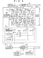
- Fig. 3 is a detailed circuit diagram of the power source device 20.
- the first power source means 21 of the power source device 20 includes a DC power source 21-1 and a snubber circuit 21-2 for intermittently cutting off a current from the DC power source 21-1.
- the second power source means 23 includes a DC power source 23-1, a voltage modulation circuit 23-2 for stabilizing a DC voltage from the DC power source 23-1, and voltage setting circuit 23-3 for setting the level of an output voltage from the voltage modulation circuit 23-2.
- the third power source means 22 includes a three-phase AC power source 22-1, a rectifier circuit coupled between power source lines PL1 and PL2 and including thyristors S1 and S12 and gate circuits G1 to G12 for triggering the thyristors S1 to S12, and a filter circuit 22-2 for smoothing a current from the rectifier circuit.
- the thyristors S1, S5 and S9 are respectively connected in series with the thyristors S2, S6 and S10 between the power source lines PL1 and PL2.
- the thyristors S3, S7 and S11 are respectively connected in series with the thyristors S4, S8 and S12 between the power source lines PL1 and PL2.
- a first-phase output terminal of the AC power source 22-1 is connected to a junction between the thyristors S1 and S2 as well as to a junction between the thyristors S3 and S4.
- a second-phase output terminal is connected to a junction between the thyristors S5 and S6 as well as to a junction between the thyristors S7 and S8.
- a third-phase output terminal is connected to a junction between the thyristors S9 and S10 as well as to a junction between thyristors S11 and S12.
- the power source device 20 further includes a control circuit 25 for synchronizing the operations of the power source means 21, 22 and 23.
- the control circuit 25 includes a pulse generator 25-1 which is coupled to the first-phase output terminal of the AC power source 22-1 and which generates a pulse every half cycle of the AC voltage, that is, every time the AC voltage at the first-phase output terminal reaches a reference level, and a ring counter 25-2 for counting an output pulse from the pulse generator 25-1 and generates count data and which is reset to "0" every time the count data reaches (M + N).
- the control circuit 25 includes a decoder 25-3, a T-type flip-flop 25-4 and AND gates 25-5 and 25-6. The decoder 25-3 receives the count data from the counter 25-2.
- the decoder 25-3 If the count value is within a range of "0" to "M-1", the decoder 25-3 generates a signal of high level. However, if the count value is within a range of "M” to "M + N-1", the decoder 25-3 generates a signal of low level from its first output terminal. Further, when the count data reaches "M + N-1", the decoder 25-3 generates a cycle pulse from its second output terminal. The output signals from the output terminals Q and Q of the flip-flop 25-4 are inverted in accordance with the cycle pulse from the decoder 25-3.
- each of the AND gates 25-5 and 25-6 On input terminal of each of the AND gates 25-5 and 25-6 is connected to the first output terminal of the decoder 25-3 and the other terminals of the AND gates 25-5 and 25-6 are respectively connected to the output terminals Q and IT of the Tflip-flop 25-4.
- An output terminal of the AND gate 25-5 is coupled to the gate circuits G1, G2, G5, G7, G9 and G10 of the thyristors S1, S2, S5, S6, S9 and S10.
- An output terminal of the AND gates 25-6 is coupled to the gate circuits G3, G4, G7, G8, G11 and G12 and the thyristors S3, S4, S7, S8, S11 and S12.
- the output terminal of the decoder 25-3 is also coupled to the snubber circuit 21-2 as well as to a switching control terminal of the voltage modulation circuit 23-2.
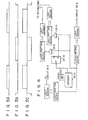
- an output voltage of 50 Hz with a waveform shown in Fig. 4A is generated from the first-phase output terminal of the AC power source 22-1.
- the pulse generator 25-1 generates a pulse signal of the waveform shown in Fig. 4B in response to an AC output voltage from the AC power source 22-1.
- the counter 25-2 counts the pulse signals generated from the pulse generator 25-1. Every time the count data reaches "101 ", for example, the cycle pulse of the waveform shown in Fig. 4C is generated from the second output terminal of the decoder 25-3.
- An output signal of high level is generated from the first output terminal of the decoder 25-3 when the count data of the counter 25-2 is within a range of "0" to "99".
- an output signal of low level is generated from the first output terminal of the decoder 25-3 when the count data is within a range of "100" and "101", as shown in Fig. 4D.
- Signals with waveforms shown in Figs. 4E and 4F, respectively, are generated from the output terminals Q and Q of the T-type flip-flop 25-4 in response to the cycle pulse with the waveform shown in Fig. 4C.
- Control signals with the waveforms respectively shown in Figs. 4G and 4H are generated from the AND gates 25-5 and 25-6.
- Each cycle signal component of the output signal from the AND gates 25-5 and 25-6 is set to high level during a time interval corresponding to 100 pulses.
- the cycle signal component is then set to low level over a time interval corresponding to 104 pulses.
- the output signals from the AND gates 25-5 and 25-6 are out of phase for a phase angle corresponding to a time interval of 102 pulses.
- a full-wave rectifier circuit constituted by the thyristors S1, S2, S5, S6, S9 and S10 is activated.
- a three-phase alternating voltage from the AC power source 22-1 is rectified and the power source lines PL1 and PL2 serve as the positive and negative power source lines, respectively.
- the heating current flows from the power source line PL1 to the power source line PL2 through the cathode 12 (Fig. 1).
- the output signals from the AND gates 25-5 and 25-6 are set to a low level, all the thyristors S1 to S12 are turned off.
- a voltage across the power sources lines PL1 and PL2 is gradually decreased as shown in Fig. 41.
- a full-wave rectifier circuit constituted by the thyristors S3, S4, S7, S8, S11 and S12 is activated.
- a three-phase alternating voltage from the AC power source 22-1 is rectified, and at this time, the power source lines PL1 and PL2 act as the negative and positive power source terminals, respectively.
- a voltage of the opposite polarity is induced across the power source lines PL1 and PL2.
- the heating current flows from the power source line PL2 to the power source line PL1 through the cathode 12.
- the snubber circuit 21-2 and the voltage modulation circuit 23-2 are controlled by an output signal of the decoder 25-3 having the waveform shown in Fig. 4D.
- the snubber circuit 21-2 causes the anode current of high level to flow to the anode 11 and the voltage modulation circuit 23-2 causes the accelerating voltage of high level set by the voltage setting circuit 23-3 to flow to the ion beam extraction electrode 13.
- the snubber circuit 21-2 interrupts the anode current and the voltage modulation circuit 23-2 prevents the DC power source 23-1 from applying the voltage to the ion beam extraction electrode 13.
- the third power sources means 22 causes the alternating heating current to flow to the cathode 12 of the ion source 10, preventing local overheating of the cathode 12.
- the service life of the cathode 12, that is, the service life of the ion source 10 can be prolonged.
- the power source means 21 and 23 interrupt the anode current and the accelerating voltage during the transition time interval, thus preventing generation of ion beams in the transition period of time.
- the third power source means 22 may be arranged to generate the heating voltage with the waveform shown in Fig. 5C in response to the output signals (corresponding to the output signals of the AND gates shown in Fig. 4G and 4H) of the AND gates shown in Figs. 5A and 5B.
- any waveform may be utilized for the heating voltage only if the high and low voltage components and a voltage level transferring component connecting the high and low voltage components during the transition time interval are included.
- control signal from the control circuit 25 is transmitted through lead wires to the power source, means 21, 22 and 23.
- the control signal from the decoder 25-3 may be converted to an optical signal. After this optical signal is converted to an electrical signal again, the signal may be supplied to the snubber circuit 21-2 and the voltage modulation circuit 23-2.
- the output signals from the AND gates 25-5 and 25-6 may be converted to optical signals. These optical signals may be converted to electrical signals again and may be applied to the gate circuits of the thyristors.
Landscapes
- Chemical & Material Sciences (AREA)
- Analytical Chemistry (AREA)
- Engineering & Computer Science (AREA)
- Combustion & Propulsion (AREA)
- Electron Sources, Ion Sources (AREA)
- Particle Accelerators (AREA)
- Generation Of Surge Voltage And Current (AREA)
Claims (8)
Applications Claiming Priority (2)
| Application Number | Priority Date | Filing Date | Title |
|---|---|---|---|
| JP56092185A JPS596024B2 (ja) | 1981-06-17 | 1981-06-17 | イオン源用電源装置 |
| JP92185/81 | 1981-06-17 |
Publications (3)
| Publication Number | Publication Date |
|---|---|
| EP0067450A2 EP0067450A2 (de) | 1982-12-22 |
| EP0067450A3 EP0067450A3 (en) | 1983-02-16 |
| EP0067450B1 true EP0067450B1 (de) | 1985-12-18 |
Family
ID=14047375
Family Applications (1)
| Application Number | Title | Priority Date | Filing Date |
|---|---|---|---|
| EP82105249A Expired EP0067450B1 (de) | 1981-06-17 | 1982-06-15 | Spannungsquelle für Lichtbogen-Ionenquelle |
Country Status (4)
| Country | Link |
|---|---|
| US (1) | US4454453A (de) |
| EP (1) | EP0067450B1 (de) |
| JP (1) | JPS596024B2 (de) |
| DE (1) | DE3268007D1 (de) |
Families Citing this family (13)
| Publication number | Priority date | Publication date | Assignee | Title |
|---|---|---|---|---|
| US4754200A (en) * | 1985-09-09 | 1988-06-28 | Applied Materials, Inc. | Systems and methods for ion source control in ion implanters |
| US4743767A (en) * | 1985-09-09 | 1988-05-10 | Applied Materials, Inc. | Systems and methods for ion implantation |
| US4825080A (en) * | 1986-03-25 | 1989-04-25 | Universite De Reims Champagne-Ardenne | Electrical particle gun |
| GB8725459D0 (en) * | 1987-10-30 | 1987-12-02 | Nat Research Dev Corpn | Generating particle beams |
| US4838021A (en) * | 1987-12-11 | 1989-06-13 | Hughes Aircraft Company | Electrostatic ion thruster with improved thrust modulation |
| JPH0772758B2 (ja) * | 1991-09-12 | 1995-08-02 | 工業技術院長 | 低エネルギー荷電粒子ビームチョッピング装置 |
| JPH0772759B2 (ja) * | 1991-09-12 | 1995-08-02 | 工業技術院長 | 低エネルギー荷電粒子ビームパルス化装置 |
| DE19522221A1 (de) * | 1995-06-20 | 1997-01-02 | Zeiss Carl Fa | Verfahren zur Regelung des Emissionsstromes einer Elektronenquelle und Elektronenquelle mit einer Regelung des Emissionsstromes |
| AUPR179500A0 (en) | 2000-11-30 | 2000-12-21 | Saintech Pty Limited | Ion source |
| US6914386B2 (en) * | 2003-06-20 | 2005-07-05 | Applied Materials Israel, Ltd. | Source of liquid metal ions and a method for controlling the source |
| US7498586B2 (en) * | 2003-10-31 | 2009-03-03 | Saintech Pty, Ltd. | Ion source control system |
| JP5955709B2 (ja) * | 2012-09-04 | 2016-07-20 | 住友重機械工業株式会社 | サイクロトロン |
| US11509130B2 (en) * | 2021-02-10 | 2022-11-22 | Qualcomm Incorporated | Disconnection arc prevention in cable-supplied power connection |
Family Cites Families (5)
| Publication number | Priority date | Publication date | Assignee | Title |
|---|---|---|---|---|
| DE823767C (de) * | 1949-03-04 | 1951-12-06 | Siemens & Halske A G | Hochvakuum-Ionenstrahlroehre mit Gluehkathode |
| DE2325786C2 (de) * | 1973-05-22 | 1983-10-06 | Leybold-Heraeus Gmbh, 5000 Koeln | Schaltung zur Regelung der Betriebsparameter eines Elektronenstrahlerzeugers |
| US3952228A (en) * | 1974-11-18 | 1976-04-20 | Ion Tech, Inc. | Electron-bombardment ion source including alternating potential means for cyclically varying the focussing of ion beamlets |
| AU522643B2 (en) * | 1977-07-15 | 1982-06-17 | Tokyo Shibaura Denki Kabushiki Kaisha | Filament heating apparatus |
| DE2844183C2 (de) * | 1978-10-10 | 1984-09-13 | Messer Griesheim Gmbh, 6000 Frankfurt | Verfahren und Einrichtung zum Einstellen des Kathodenheizstromes in einem technischen Elektronenstrahl-Gerät |
-
1981
- 1981-06-17 JP JP56092185A patent/JPS596024B2/ja not_active Expired
-
1982
- 1982-06-09 US US06/386,529 patent/US4454453A/en not_active Expired - Fee Related
- 1982-06-15 DE DE8282105249T patent/DE3268007D1/de not_active Expired
- 1982-06-15 EP EP82105249A patent/EP0067450B1/de not_active Expired
Also Published As
| Publication number | Publication date |
|---|---|
| US4454453A (en) | 1984-06-12 |
| JPS57208029A (en) | 1982-12-21 |
| EP0067450A3 (en) | 1983-02-16 |
| JPS596024B2 (ja) | 1984-02-08 |
| DE3268007D1 (en) | 1986-01-30 |
| EP0067450A2 (de) | 1982-12-22 |
Similar Documents
| Publication | Publication Date | Title |
|---|---|---|
| EP0067450B1 (de) | Spannungsquelle für Lichtbogen-Ionenquelle | |
| EP0230850B1 (de) | Hochspannungsimpulsgenerator | |
| JPH04138068A (ja) | インバータ装置の駆動回路 | |
| JP3581809B2 (ja) | インバータ | |
| US3430123A (en) | Rectifier-inverter motor power supply | |
| JPS5937174B2 (ja) | 放電加工電源 | |
| US4909812A (en) | Device for power supply of gas-cleaning electrical precipitators | |
| US4857810A (en) | Current interruption operating circuit for a gaseous discharge lamp | |
| US3944780A (en) | Power supply source for arc welding | |
| EP0129909B1 (de) | Methode und Gerät zum Steuern eines rückwärts leitenden über die Steuerelektrode sperrbaren Thyristors | |
| US3621355A (en) | Double half wave motor control | |
| CA1050099A (en) | High frequency power supply for corona generator | |
| JPH0666663B2 (ja) | パルス高電圧発生装置 | |
| RU2207191C2 (ru) | Способ питания электрофильтра и устройство для его реализации | |
| US3406329A (en) | Parallel inverter with rapid response time to changes in pulse durations | |
| SU873375A1 (ru) | Устройство дл управлени тиристорным преобразователем | |
| JPS59139890A (ja) | 交流モ−タ−の入力制御方法及び回路装置 | |
| SU1382493A1 (ru) | Устройство дл питани электрофильтра знакопеременным напр жением | |
| US2650305A (en) | Converter and other electrical apparatus with rotary commutators | |
| RU2161362C1 (ru) | Делитель напряжения | |
| GB2126024A (en) | Waveform generator | |
| CN1032122A (zh) | 气体净化电滤器的电源装置 | |
| SU608632A1 (ru) | Тиристорный генератор дл электроэрозионных станков | |
| SU813735A1 (ru) | Формирователь одиночных импульсов | |
| JPH0647082B2 (ja) | 電気集じん装置の荷電方法 |
Legal Events
| Date | Code | Title | Description |
|---|---|---|---|
| PUAI | Public reference made under article 153(3) epc to a published international application that has entered the european phase |
Free format text: ORIGINAL CODE: 0009012 |
|
| PUAL | Search report despatched |
Free format text: ORIGINAL CODE: 0009013 |
|
| 17P | Request for examination filed |
Effective date: 19820712 |
|
| AK | Designated contracting states |
Designated state(s): CH DE FR GB LI |
|
| AK | Designated contracting states |
Designated state(s): CH DE FR GB LI |
|
| RAP1 | Party data changed (applicant data changed or rights of an application transferred) |
Owner name: KABUSHIKI KAISHA TOSHIBA |
|
| GRAA | (expected) grant |
Free format text: ORIGINAL CODE: 0009210 |
|
| AK | Designated contracting states |
Designated state(s): CH DE FR GB LI |
|
| REF | Corresponds to: |
Ref document number: 3268007 Country of ref document: DE Date of ref document: 19860130 |
|
| ET | Fr: translation filed | ||
| PLBE | No opposition filed within time limit |
Free format text: ORIGINAL CODE: 0009261 |
|
| STAA | Information on the status of an ep patent application or granted ep patent |
Free format text: STATUS: NO OPPOSITION FILED WITHIN TIME LIMIT |
|
| 26N | No opposition filed | ||
| REG | Reference to a national code |
Ref country code: GB Ref legal event code: 746 |
|
| PGFP | Annual fee paid to national office [announced via postgrant information from national office to epo] |
Ref country code: GB Payment date: 19910605 Year of fee payment: 10 |
|
| PGFP | Annual fee paid to national office [announced via postgrant information from national office to epo] |
Ref country code: CH Payment date: 19910611 Year of fee payment: 10 |
|
| PGFP | Annual fee paid to national office [announced via postgrant information from national office to epo] |
Ref country code: FR Payment date: 19910619 Year of fee payment: 10 |
|
| PGFP | Annual fee paid to national office [announced via postgrant information from national office to epo] |
Ref country code: DE Payment date: 19910628 Year of fee payment: 10 |
|
| PG25 | Lapsed in a contracting state [announced via postgrant information from national office to epo] |
Ref country code: GB Effective date: 19920615 |
|
| PG25 | Lapsed in a contracting state [announced via postgrant information from national office to epo] |
Ref country code: LI Effective date: 19920630 Ref country code: CH Effective date: 19920630 |
|
| GBPC | Gb: european patent ceased through non-payment of renewal fee |
Effective date: 19920615 |
|
| PG25 | Lapsed in a contracting state [announced via postgrant information from national office to epo] |
Ref country code: FR Effective date: 19930226 |
|
| REG | Reference to a national code |
Ref country code: CH Ref legal event code: PL |
|
| PG25 | Lapsed in a contracting state [announced via postgrant information from national office to epo] |
Ref country code: DE Effective date: 19930302 |
|
| REG | Reference to a national code |
Ref country code: FR Ref legal event code: ST |