EP0067637A2 - Gewichtsdetektionsschaltkreis für eine einen Druckaufnehmer aufweisende Waage - Google Patents
Gewichtsdetektionsschaltkreis für eine einen Druckaufnehmer aufweisende Waage Download PDFInfo
- Publication number
- EP0067637A2 EP0067637A2 EP82302920A EP82302920A EP0067637A2 EP 0067637 A2 EP0067637 A2 EP 0067637A2 EP 82302920 A EP82302920 A EP 82302920A EP 82302920 A EP82302920 A EP 82302920A EP 0067637 A2 EP0067637 A2 EP 0067637A2
- Authority
- EP
- European Patent Office
- Prior art keywords
- load cell
- resistance
- weight detection
- detection circuit
- bridge circuit
- Prior art date
- Legal status (The legal status is an assumption and is not a legal conclusion. Google has not performed a legal analysis and makes no representation as to the accuracy of the status listed.)
- Granted
Links
Images
Classifications
-
- G—PHYSICS
- G01—MEASURING; TESTING
- G01G—WEIGHING
- G01G23/00—Auxiliary devices for weighing apparatus
- G01G23/18—Indicating devices, e.g. for remote indication; Recording devices; Scales, e.g. graduated
- G01G23/36—Indicating the weight by electrical means, e.g. using photoelectric cells
-
- G—PHYSICS
- G01—MEASURING; TESTING
- G01G—WEIGHING
- G01G3/00—Weighing apparatus characterised by the use of elastically-deformable members, e.g. spring balances
- G01G3/12—Weighing apparatus characterised by the use of elastically-deformable members, e.g. spring balances wherein the weighing element is in the form of a solid body stressed by pressure or tension during weighing
- G01G3/14—Weighing apparatus characterised by the use of elastically-deformable members, e.g. spring balances wherein the weighing element is in the form of a solid body stressed by pressure or tension during weighing measuring variations of electrical resistance
- G01G3/142—Circuits specially adapted therefor
Definitions
- This invention relates to a weight detection circuit for a load cell scale.
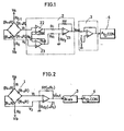
- a conventional weight detection circuit for the load cell scale gives an output of a bridge circuit 1 of a strain gauge resistance stuck to the load cell, that is, analog voltage proportional to weight, into a high-input-impedance differential amplifier 2 (e.g., an instrumentation amplifier), the output being given to an A-D converter 4 through a bias circuit 3.
- resistances R0 at the bridge circuit 1 serve as temperature- compensating resistances for the load cell.
- an output voltage V ou t of the high-input-impedance differential amplifier 2 is represented by the following equation: where V 1 , V 2 : output voltages of bridge circuit 1, and a: an amplification factor of high-input-impedance differential amplifier 2.
- a node equation is set up at each node of bridge circuit 1 and solved to obtain the following equation: where R: strain gauge resistance at zero weight, ⁇ R: resistance changing in proportion to weight, V a , V b : applied voltage, and
- Equation 2 temperature compensating resistance
- the weight detection circuit for the load cell scale is constructed as the above, since the output of bridge circuit 1 is amplified by the high-input-impedance differential amplifier 2, the circuit 2 is assumed independent, so that the temperature characteristics of (a) four strain gauge resistances (R ⁇ ⁇ R) at the bridge circuit 1, (b) a feedback resistance R f and an input resistance Ri at the high-input-impedance differential amplifier 2, (c) two voltage-dividing resistances Rdl and Rd2 thereof, and (d) three resistances R bl , R b2 and R b3 at the amplifier 2, are enough to be unified at each group (a), (b), (c) or (d), but need not be unified as a whole, thereby facilitating the design.
- the number of parts increases so that the conventional weight detection circuit is defective in a high manufacturing cost.
- This invention is characterized mainly in that an operational amplifier is connected directly to an output of a bridge circuit for a strain gauge resistance stuck to a load cell, and that a feedback resistance is made equivalent to a voltage-dividing resistance at the ground side so that a circuit equivalent to a differential amplifier having an amplification factor of R (where R : a reference resistance value of strain gauge resistance when the weight is zero, and R l : feedback resistance or voltage-dividing resistance at the ground side) is provided.
- R a reference resistance value of strain gauge resistance when the weight is zero
- R l feedback resistance or voltage-dividing resistance at the ground side
- One object of the invention is to provide a weight detection circuit constructed as foregoing, thereby simplifying the conventional differential amplifier to lead to simplification of the weight detection circuit as a whole and a low manufacturing cost.
- this invention is characterized in that a bias resistance is connected to the bridge circuit of load cell at ⁇ the weight detection circuit constructed as foregoing so that the predetermined bias voltage which is derived from the node equation can be obtained, whereby the bias circuit as well as the high-input-impedance differential amplifier is intended to be simplified, thus simplifying the weight detection circuit as a whole and reducing the manufacturing cost.
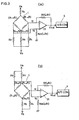
- an operational amplifiers 22 and 23 resistances R bl , R b2 and Rb3, input resistance Ri, and voltage-dividing resistance R dl at the non-ground side, and omitted from a high-impedance-input differential amplifier 2 shown in Fig. 1, and a feedback resistance R f is made equal in resistance value,to a voltage-dividing resistance Rd2 at the ground side.
- a feedback resistance R f is made equal in resistance value,to a voltage-dividing resistance Rd2 at the ground side.
- Equation 5 When Equation 5 is compared with Equation 3 it is understandable that this circuit acts as a differential amplifier of the equivalent amplification factor of .
- This invention also is necessary to define the temperature characteristics of each strain gauge resistance at the bridge circuit, feedback res;stance R f at the operational amplifier 21 side, and voltage-dividing resistance R d2 .
- the strain gauge resistance is generally superior in the temperature characteristic.
- the conventional strain gauge resistance is used as it is, so that the feedback resistance R f and voltage-dividing resistance R d2 are allowed to coincide in temperature characteristic with the strain gauge resistance, thereby obtaining a weight detection circuit extremely superior in the temperature characteristic as a whole and saving the number of parts.
- a bias circuit 3 at the last stage also is omitted from the Fig. 2 embodiment, in which the bridge circuit 1 is connected at its two output lines with applied voltages V a and V b though bias resistances R 3 and R 4 .
- V a and V b are used as the bias power source.
- the node equation is set up at each node of bridge circuit 1 and solved to obtain an output voltage V'out of operational amplifier 21 as follows: where, R 2 is neglected due to R 2 >> ⁇ R 2 , then is obtained. Since lst term in Equation 7 is equal to Equation 6, this term represents an amplified voltage of weight signal component and 2nd and 3rd terms are constant to represent bias voltage. The 4th term including ⁇ R represents an error voltage. Thenm an error rate ⁇ is obtained by use of a ratio of the lst term to the 4th term, as follows:
- Equation 9 represents at the lst term amplified voltage for the weight signal component, at the 2nd and 3rd terms bias voltage, and at the 4th term an error voltage.
- a ratio of lst term to 4th term, i.e., an error rate e is obtained similarly to Equation 8so that R 1 , R 3 and R 4 may be selected to make the error rate ⁇ smaller than the accuracy of the scale.
- Equations 7 and 9 are rearranged to replace the 2nd and 3rd terms by respectively, in which V xl represents an applied voltage at the resistance R 4 connected side and V x 2 represents that at the resistance R 4 connected side.
- two bias-resistances R 3 and R 4 have to be selected not to affect the temperature characteristic of the strain gauge resistance.
- the weight detection circuit for the load cell scale of the invention can simplify the high-input-impedance differential amplifier to thereby simplify the weight detection circuit, lower the manufacturing cost, and further,simplify the bias circuit, thus improving the aforesaid effect.
Landscapes
- Physics & Mathematics (AREA)
- General Physics & Mathematics (AREA)
- Measurement Of Length, Angles, Or The Like Using Electric Or Magnetic Means (AREA)
- Measurement Of Force In General (AREA)
- Arrangements For Transmission Of Measured Signals (AREA)
Applications Claiming Priority (2)
| Application Number | Priority Date | Filing Date | Title |
|---|---|---|---|
| JP56093129A JPS57207831A (en) | 1981-06-16 | 1981-06-16 | Weight detecting circuit of load-cell type weighing apparatus |
| JP93129/81 | 1981-06-16 |
Publications (3)
| Publication Number | Publication Date |
|---|---|
| EP0067637A2 true EP0067637A2 (de) | 1982-12-22 |
| EP0067637A3 EP0067637A3 (en) | 1984-06-06 |
| EP0067637B1 EP0067637B1 (de) | 1989-05-24 |
Family
ID=14073904
Family Applications (1)
| Application Number | Title | Priority Date | Filing Date |
|---|---|---|---|
| EP82302920A Expired EP0067637B1 (de) | 1981-06-16 | 1982-06-07 | Gewichtsdetektionsschaltkreis für eine einen Druckaufnehmer aufweisende Waage |
Country Status (6)
| Country | Link |
|---|---|
| US (1) | US4475608A (de) |
| EP (1) | EP0067637B1 (de) |
| JP (1) | JPS57207831A (de) |
| AU (1) | AU552867B2 (de) |
| DE (1) | DE3279713D1 (de) |
| IL (1) | IL66041A (de) |
Cited By (2)
| Publication number | Priority date | Publication date | Assignee | Title |
|---|---|---|---|---|
| EP0145433A3 (en) * | 1983-12-03 | 1986-04-16 | Kabushiki Kaisha Ishida Koki Seisakusho | Electronic weigher |
| KR100238390B1 (ko) * | 1997-05-23 | 2000-01-15 | 박재범 | 압력센서의 온도 보상 회로 |
Families Citing this family (3)
| Publication number | Priority date | Publication date | Assignee | Title |
|---|---|---|---|---|
| US4722406A (en) * | 1985-06-21 | 1988-02-02 | Ishida Scales Mfg. Co. Ltd. | Electronic weigher with compensated test signal |
| JP7451439B2 (ja) * | 2021-01-27 | 2024-03-18 | 日立グローバルライフソリューションズ株式会社 | 冷蔵庫 |
| CN115248575A (zh) * | 2022-02-15 | 2022-10-28 | 郑州大学第一附属医院 | 一种药房用agv控制系统及方法 |
Family Cites Families (5)
| Publication number | Priority date | Publication date | Assignee | Title |
|---|---|---|---|---|
| US3831687A (en) * | 1970-07-13 | 1974-08-27 | Nat Controls | Flexure base scale |
| GB1510027A (en) * | 1975-10-10 | 1978-05-10 | Railweight Inc Ltd | Electronic weighing systems |
| US4055078A (en) * | 1976-07-01 | 1977-10-25 | Antonio Nicholas F D | Strain transducer |
| US4177868A (en) * | 1978-01-30 | 1979-12-11 | Bio-Dynamics Inc. | Weight-measuring and display device |
| DE2842041A1 (de) * | 1978-09-27 | 1980-04-10 | Siemens Ag | Verfahren zur korrektur der empfindlichkeit der auswaegeeinrichtung von elektrischen waegeanlagen und schaltungsanordnung zur ausuebung des verfahrens |
-
1981
- 1981-06-16 JP JP56093129A patent/JPS57207831A/ja active Granted
-
1982
- 1982-06-04 US US06/385,123 patent/US4475608A/en not_active Expired - Lifetime
- 1982-06-07 DE DE8282302920T patent/DE3279713D1/de not_active Expired
- 1982-06-07 EP EP82302920A patent/EP0067637B1/de not_active Expired
- 1982-06-11 AU AU84851/82A patent/AU552867B2/en not_active Ceased
- 1982-06-11 IL IL66041A patent/IL66041A/xx unknown
Cited By (2)
| Publication number | Priority date | Publication date | Assignee | Title |
|---|---|---|---|---|
| EP0145433A3 (en) * | 1983-12-03 | 1986-04-16 | Kabushiki Kaisha Ishida Koki Seisakusho | Electronic weigher |
| KR100238390B1 (ko) * | 1997-05-23 | 2000-01-15 | 박재범 | 압력센서의 온도 보상 회로 |
Also Published As
| Publication number | Publication date |
|---|---|
| AU552867B2 (en) | 1986-06-26 |
| IL66041A (en) | 1985-12-31 |
| DE3279713D1 (en) | 1989-06-29 |
| IL66041A0 (en) | 1982-09-30 |
| AU8485182A (en) | 1982-12-23 |
| EP0067637A3 (en) | 1984-06-06 |
| JPH0461287B2 (de) | 1992-09-30 |
| JPS57207831A (en) | 1982-12-20 |
| EP0067637B1 (de) | 1989-05-24 |
| US4475608A (en) | 1984-10-09 |
Similar Documents
| Publication | Publication Date | Title |
|---|---|---|
| US5515737A (en) | Weighing apparatus | |
| DE3007142C2 (de) | Halbleiter-Druckaufnehmervorrichtung mit Nullpunkt-Temperaturkompensation | |
| US4404539A (en) | Semiconductor strain gauge | |
| EP0176173B1 (de) | Fühleranordnung zum Messen von drei senkrechten Kräften und drei senkrechten Momenten | |
| US4169243A (en) | Remote sensing apparatus | |
| EP0068900B1 (de) | Differenzverstärker mit einem Tiefpassfilter | |
| JPS58140604A (ja) | 温度補償回路付き集積化センサ | |
| EP0299806B1 (de) | Wägeapparat mit Dehnungsmessstreifen | |
| US4229692A (en) | Linear low drift bridge amplifier | |
| US4261195A (en) | Transducer bridge circuit arrangement and method | |
| US3971984A (en) | Wide-range logarithmic responding translation circuit | |
| CN107144330A (zh) | 一种双孔悬臂梁应变片的动态电子小型无人车衡 | |
| US4475608A (en) | Weight detection circuit for a load cell scale | |
| CN210833946U (zh) | 测力传感器的组桥电路 | |
| US4071823A (en) | Two-wire type amplifier | |
| CA1117598A (en) | Bridge circuit | |
| CN106289464A (zh) | 一种两线制微弱应变电桥信号变送器 | |
| CN114812915A (zh) | 一种压力扫描阀电路 | |
| US4492122A (en) | Circuit for linearization of transducer | |
| CN217278608U (zh) | 一种电流采样电路 | |
| US20250314680A1 (en) | Voltage detection circuit, voltage monitoring circuit, and power supply and control circuit thereof | |
| SU900132A1 (ru) | Тензометрический преобразователь | |
| CN116558679A (zh) | 偏压消除电路和压力测量电路 | |
| CA1165140A (en) | Temperature sensing circuit | |
| SU1714335A1 (ru) | Тензопреобразователь |
Legal Events
| Date | Code | Title | Description |
|---|---|---|---|
| PUAI | Public reference made under article 153(3) epc to a published international application that has entered the european phase |
Free format text: ORIGINAL CODE: 0009012 |
|
| AK | Designated contracting states |
Designated state(s): CH DE FR GB IT LI NL SE |
|
| 17P | Request for examination filed |
Effective date: 19830614 |
|
| PUAL | Search report despatched |
Free format text: ORIGINAL CODE: 0009013 |
|
| AK | Designated contracting states |
Designated state(s): CH DE FR GB IT LI NL SE |
|
| AK | Designated contracting states |
Designated state(s): CH DE FR GB IT LI NL SE |
|
| GRAA | (expected) grant |
Free format text: ORIGINAL CODE: 0009210 |
|
| AK | Designated contracting states |
Kind code of ref document: B1 Designated state(s): CH DE FR GB IT LI NL SE |
|
| ITF | It: translation for a ep patent filed | ||
| PGFP | Annual fee paid to national office [announced via postgrant information from national office to epo] |
Ref country code: SE Payment date: 19890616 Year of fee payment: 8 Ref country code: CH Payment date: 19890616 Year of fee payment: 8 |
|
| REF | Corresponds to: |
Ref document number: 3279713 Country of ref document: DE Date of ref document: 19890629 |
|
| PGFP | Annual fee paid to national office [announced via postgrant information from national office to epo] |
Ref country code: NL Payment date: 19890630 Year of fee payment: 8 |
|
| ET | Fr: translation filed | ||
| PLBE | No opposition filed within time limit |
Free format text: ORIGINAL CODE: 0009261 |
|
| STAA | Information on the status of an ep patent application or granted ep patent |
Free format text: STATUS: NO OPPOSITION FILED WITHIN TIME LIMIT |
|
| 26N | No opposition filed | ||
| PG25 | Lapsed in a contracting state [announced via postgrant information from national office to epo] |
Ref country code: SE Effective date: 19900608 |
|
| PG25 | Lapsed in a contracting state [announced via postgrant information from national office to epo] |
Ref country code: LI Effective date: 19900630 Ref country code: CH Effective date: 19900630 |
|
| PG25 | Lapsed in a contracting state [announced via postgrant information from national office to epo] |
Ref country code: NL Effective date: 19910101 |
|
| NLV4 | Nl: lapsed or anulled due to non-payment of the annual fee | ||
| REG | Reference to a national code |
Ref country code: CH Ref legal event code: PL |
|
| ITTA | It: last paid annual fee | ||
| EUG | Se: european patent has lapsed |
Ref document number: 82302920.2 Effective date: 19910206 |
|
| PGFP | Annual fee paid to national office [announced via postgrant information from national office to epo] |
Ref country code: GB Payment date: 19980529 Year of fee payment: 17 |
|
| PGFP | Annual fee paid to national office [announced via postgrant information from national office to epo] |
Ref country code: FR Payment date: 19980609 Year of fee payment: 17 |
|
| PGFP | Annual fee paid to national office [announced via postgrant information from national office to epo] |
Ref country code: DE Payment date: 19980612 Year of fee payment: 17 |
|
| PG25 | Lapsed in a contracting state [announced via postgrant information from national office to epo] |
Ref country code: GB Free format text: LAPSE BECAUSE OF NON-PAYMENT OF DUE FEES Effective date: 19990607 |
|
| PG25 | Lapsed in a contracting state [announced via postgrant information from national office to epo] |
Ref country code: FR Free format text: THE PATENT HAS BEEN ANNULLED BY A DECISION OF A NATIONAL AUTHORITY Effective date: 19990630 |
|
| GBPC | Gb: european patent ceased through non-payment of renewal fee |
Effective date: 19990607 |
|
| PG25 | Lapsed in a contracting state [announced via postgrant information from national office to epo] |
Ref country code: DE Free format text: LAPSE BECAUSE OF NON-PAYMENT OF DUE FEES Effective date: 20000503 |
|
| REG | Reference to a national code |
Ref country code: FR Ref legal event code: ST |