EP0067686A2 - Energieversorgungseinrichtung für einen Zerstäuber in einem Atomabsorptionsmesser - Google Patents
Energieversorgungseinrichtung für einen Zerstäuber in einem Atomabsorptionsmesser Download PDFInfo
- Publication number
- EP0067686A2 EP0067686A2 EP82303039A EP82303039A EP0067686A2 EP 0067686 A2 EP0067686 A2 EP 0067686A2 EP 82303039 A EP82303039 A EP 82303039A EP 82303039 A EP82303039 A EP 82303039A EP 0067686 A2 EP0067686 A2 EP 0067686A2
- Authority
- EP
- European Patent Office
- Prior art keywords
- current
- cuvette
- output signal
- negative feedback
- supply device
- Prior art date
- Legal status (The legal status is an assumption and is not a legal conclusion. Google has not performed a legal analysis and makes no representation as to the accuracy of the status listed.)
- Withdrawn
Links
Images

Classifications
-
- G—PHYSICS
- G05—CONTROLLING; REGULATING
- G05D—SYSTEMS FOR CONTROLLING OR REGULATING NON-ELECTRIC VARIABLES
- G05D23/00—Control of temperature
- G05D23/19—Control of temperature characterised by the use of electric means
- G05D23/1906—Control of temperature characterised by the use of electric means using an analogue comparing device
-
- G—PHYSICS
- G01—MEASURING; TESTING
- G01N—INVESTIGATING OR ANALYSING MATERIALS BY DETERMINING THEIR CHEMICAL OR PHYSICAL PROPERTIES
- G01N21/00—Investigating or analysing materials by the use of optical means, i.e. using sub-millimetre waves, infrared, visible or ultraviolet light
- G01N21/62—Systems in which the material investigated is excited whereby it emits light or causes a change in wavelength of the incident light
- G01N21/71—Systems in which the material investigated is excited whereby it emits light or causes a change in wavelength of the incident light thermally excited
- G01N21/74—Systems in which the material investigated is excited whereby it emits light or causes a change in wavelength of the incident light thermally excited using flameless atomising, e.g. graphite furnaces
-
- G—PHYSICS
- G05—CONTROLLING; REGULATING
- G05F—SYSTEMS FOR REGULATING ELECTRIC OR MAGNETIC VARIABLES
- G05F1/00—Automatic systems in which deviations of an electric quantity from one or more predetermined values are detected at the output of the system and fed back to a device within the system to restore the detected quantity to its predetermined value or values, i.e. retroactive systems
- G05F1/66—Regulating electric power
Definitions
- This invention relates to a power supply device for an atomizer used in an atomic absorptiometer, and more particularly to a power supply device supplying power to such an atomizer in which a cuvette of resistance heating type is employed for atomizing a sample.
- an atomizer is generally provided for atomizing a sample to be subjected to measurement, and a beam of light having a wavelength spectrum selected depending on an element to be analyzed in the sample subjected to measurement is directed toward the sample atomized by the atomizer, so that the element contained in the sample can be quantitatively analyzed on the basis of the absorption coefficient of the sample absorbing a predetermined wavelength component of light directed thereto.
- a cuvette of resistance heating type made of graphite is customarily employed in such an atomizer.
- the level of electric power supplied to the cuvette is varied to raise stepwise the temperature of the cuvette from a low level to a high level to thereby sequentially carry out the stages of sample drying and ashing in order to eliminate unnecessary components of the sample, and, then, the temperature of the cuvette is further raised to carry out.
- the stage of atomizing In this case, the temperature levels in the individual stages and the durations of these stages are controlled according to a pre-set program selected depending on the factors including the form of the sample and the kind of the element to be analyzed, so that the particular element can be accurately quantitatively analyzed.
- a power supply device comprising current control means capable of maintaining the current supplied to the cuvette of resistance heating type at a predetermined constant level has been customarily employed in the field of art.
- the cuvette is heated in the atomizing stage up to a temperature as high as, for example, about 3,000° although it differs depending on the sample, the material of the cuvette, for example, graphite is consumed after a long time of use at such a high temperature, and its resistance value varies inevitably. Consequently, the prior art current control means provided for maintaining constant the current supplied to the cuvette is no more effective for maintaining constant the power supplied to the cuvette, and the resultant variation of the temperature of the sample makes impossible the accurate quantitative analysis of the particular element.
- a power supply device for an atomizer used in an atomic absorptiometer which device comprises means for monitoring the power supplied to the atomizer in the atomic absorptiometer and means for automatically or manually regulating, on the basis of the result of monitoring, the current supplied to the cuvette by a constant current controlling circuit in the atomizer, whereby to maintain constant the power level supplied to the atomizer.
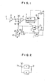
- a current setting signal indicative of a given setting of current to be supplied to a cuvette 9 is applied to an input terminal 1.
- This current setting signal is applied through the input terminal 1 to an input amplifier 2, and the output signal from the input amplifier 2 is applied through a resistor 3 to one of the input terminals of an adder 30.
- a current signal indicative of the value of current being actually supplied to the cuvette 9 is applied to the other input terminal of the adder 30, as described later.
- the output signal from the adder 30 is thus indicative of the difference between the two inputs and is applied to a differential amplifier 4.
- the output terminal of the differential amplifier 4 is connected through a pulse generator 7 to the gate of a thyristor 8 to control the turn-on phase angle of the thyristor 8.
- this thyristor 8 may be either a unilateral one or a bilateral one, the thyristor 8 employed in this embodiment is of the bilateral type, for example, a triac.
- the pulse generator 7 In response to the application of the output signal from the differential amplifier 4, the pulse generator 7 generates one pulse in each of the positive and negative half cycles of an AC voltage from an AC power source 6 at the phase angle corresponding to the level of the output signal from the differential amplifier 4.
- the thyristor 8 is turned on, and the power source 6 supplies current to the cuvette 9 through the turned-on thyristor 8.
- the AC current supplied to the cuvette 9 is detected by a current detector 10, for example, a current transformer and is converted into a DC current by a current rectifier 11.
- the current signal indicative of the current being supplied to the cuvette 9 is applied to the other input terminal of the adder 30 through a variable resistor 16 and the resistor 5.
- the difference signal appearing from the adder 30 is applied to the pulse generator 7 after being amplified by the differential amplifier 4.
- the phase of the pulse signal generated from the pulse generator 7 is delayed to delay the turn-on phase angle of the thyristor 8, with the result that the value of the current supplied to the cuvette 9 decreases until it becomes equal to the setting.
- the structure above described is generally similar to that of the prior art power supply device including the known constant current control circuit.
- the present invention is featured by the fact that it further comprises means for monitoring the power supplied to the cuvette 9.
- This monitoring means includes a voltage rectifier 13 converting the AC voltage applied across the cuvette 9 into a DC voltage for producing a voltage signal V indicative of the AC voltage applied across the cuvette 9, a multiplier 14 multiplying the current signal I, which is indicative of the cuvette current detected by the current detector 10 and rectified by the rectifier 11, by the voltage signal V applied from the rectifier 13, and an indicator or meter 12 indicating the output signal from the multiplier 14.
- the meter 12 is preferably of the dual scale type so that both of the output from the multiplier 14 and the output from the current rectifier 11 can be monitored.
- a change-over switch 15 is provided so that the output from the current rectifier 11 can be read on one of the scales of the meter 12 in the position in which the switch 15 connects its terminal A to the input terminal C of the meter 12, and the output from the multiplier 14 can be read on the other scale in the position in which its terminal B is connected to the input terminal C of the meter 12.
- the switch 15 is connected at its terminal A to the input terminal C of the meter 12, and the current supplied to the cuvette 9 is controlled to be maintained constant while monitoring the cuvette current by the reading on the meter 12.
- the cuvette 9 heated up to a very high temperature in the atomizing stage is consumed progressively after a long time of use, and its resistance value varies to vary the amount of power to be supplied thereto. It is therefore desirable to carry out necessary adjustment before a series of measurement steps are started so that the power of predetermined regulated level can always be supplied to the cuvette 9. This regulation is done in this embodiment in a manner as will be described presently.
- the switch 15 is connected at its terminal B to the input terminal C of the meter 12 so as to indicate the output from the multiplier 14 on the meter 12.
- a current is supplied to the cuvette 9 as usual.
- the output signal from the multiplier 14 represents the product VI of the voltage signal V indicative of the voltage applied across the cuvette 9 and the current signal I indicative of the cuvette current, and this product VI corresponds to the power supplied to the cuvette 9. Therefore, the variable resistor 16 is suitably adjusted until the meter 12 indicates the predetermined power value.
- the current regulator circuit shown in FIG. 1 is equivalently expressed by a circuit as shown in FIG. 2.
- the symbols I , I , G and a represent the current setting signal applied to the input terminal 1 in FIG. 1, the cuvette current, the gain of the circuit, and the feedback factor of the negative feedback circuit, respectively, and the following relation holds:
- Power consumption W of the cuvette 9 is given by I c 2 R, where R is the resistance of the cuvette 9.
- R is the resistance of the cuvette 9.
- the switch 15 is changed over to the position connected at its terminal B to the input terminal C of the meter 12 prior to or during the process of measurement of a sample, and, while reading the value of power supplied to the cuvette 9 on the meter 12, the variable resistor 16 is suitably adjusted until the power of predetermined regulated level is supplied to the cuvette 9.
- the increment of power supplied to the cuvette 9 (the temperature increment) due to the variation of the resistance value of the cuvette 9 resulting from the consumption of the cuvette 9 can be compensated so as to maintain constant the level of power supplied to the cuvette 9.
- This emboidment is therefore advantageous in that the accuracy of measurement of a sample can be improved, and wasteful power consumption of the cuvette 9 can be saved to extend the useful service life of the cuvette 9.
- the increment of power is compensated prior to or during the process of sample measurement by adjusting the variable resistor 16 for compensating the variation of the resistance value of the cuvette 9.
- This embodiment is therefore also advantageous in that the accuracy of the resistance value of the cuvette 9 need not be strictly specified, thereby simplifying the process control of the cuvette 9 and reducing the cost of manufacture of the cuvette 9.
- the adjusting range of the variable resistor 16 is correspondingly widened.
- the variable resistor 16 is not adjusted any more and the cuvette 9 is replaced by a new one when the adjusting range of the variable resistor 16 reaches a limit provided by a stopper.
- This embodiment is therefore also advantageous in that the maintenance and inspection of the cuvette 9 is facilitated because the time of replacement of the cuvette 9 can be clearly indicated.
- variable resistor 16 in the feedback circuit is utilized as means for compensating the increment of current supplied to the cuvette 9
- the effect similar to that described above can be achieved by making variable the resistor 3 connected to the input amplifier 2 amplifying the current setting signal I or by making variable the gain of the input amplifier 2 (corresponding to regulation of I in the equation (1)).
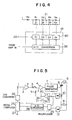
- FIG. 3 is a circuit diagram of another embodiment of the power supply device according to the present invention.
- the same reference numerals are used to designate the same or equivalent parts appearing in FIG. 1.
- variable resistor 16 in the first embodiment shown in FIG. 1 is arranged to be automatically adjusted so as to automatically regulate the power value indicated on the meter 12.
- the variable resistor 16 shown in FIG. 1 is replaced by a current compensation circuit 17 enclosed by dotted lines.
- This current compensation circuit 17 includes a differential amplifier 18, an A/D converter 19 and a variable-gain amplifier 36.
- the difference signal indicative of the difference between the current setting signal applied to the input terminal 1 and the output signal from the multiplier 14 is applied through an adder 42 to one of the input terminals of the differential amplifier 18 which is grounded at the other input terminal and connected at its output terminal to the A/D converter 19.
- the variable-gain amplifier 36 includes a fixed-gain amplifier 20 and a gain-regurating variable resistor 21 and is thus of the known type in which the gain of the amplifier 36 can be varied by varying the resistance value of the variable resistor 21.
- the differential amplifier 18 amplifies the difference signal which is indicative of the difference between the current setting signal applied to the input terminal 1 and the output signal from the multiplier 14 and which is regulated as described later, and its analog output signal is converted into a digital signal by the A/D converter 19.
- the A/D converter 19 includes an A/D conversion circuit 38 and a latch circuit 40.
- the latch circuit 40 latches and holds the digital signal generated and applied from the A/D conversion circuit 38 at that time. The contents of the latch circuit 40 remain unchanged until the next actuating signal is applied to its input terminal 22.
- the variable resistor 21 includes a plurality of resistor elements R 0 , R 1 , R 2 , R 3 and R 4 connected in series, and a plurality of normally-closed switches S 1 , S 2 , S 3 and S 4 are connected in parallel with the resistor elements R 1 , R 2 , R 3 and R 4 respectively.
- the resistor elements R 1 , R 2 , R 3 and R 4 are provided to correspond to the individual digits D 1 , D 2 , D 3 and D 4 respectively constituting a binary digital signal latched by the latch circuit 40 in the A/D converter 19.
- the corresponding one of the switches S connected in parallel therewith is opened from the closed position.
- the binary ditital signal latched by the latch circuit 40 is reprsented by four bits "1001"
- the switches S 1 and S 4 are opened whereas the switches S 2 and S 3 remain closed. Consequently, the resistance value of the variable resistor 21 is given by R + R 2 + R 3 in such a case.
- the input terminal of the differential amplifier 18 is connected to the output terminal of the adder 42 which generates the difference signal indicative of the difference between the current setting signal applied to the input terminal 1 and the output signal of the multiplier 14 indicative of the power consumption of the cuvette 9.
- the level of the output signal from the multiplier 14 and the resistance values of resistors 32 and 34 in the differential amplifier 18 are so regulated that the output signal from the adder 42 is substantially null.
- the level of the output signal from the multiplier 14 and the resistance values of the resistors 32 and 34 are initially so regulated.
- the differential amplifier 18 when the resistance of the cuvette 9 increases to vary its power consumption progressively due to progressive consumption of the cuvette 9, the differential amplifier 18 generates its output signal indicative of the increment of power consumption, and the A/D converter 19 converts such an analog signal into the corresponding digital signal.
- One or more of the switches S selected depending on the digital value are opened to increase the resistance value of the variable resistor 21 thereby increasing the gain of the variable-gain amplifier 36. This means that, the value of a in the equation (1) increases to decrease the value of I , so that the power consumption is regulated to be equal to the predetermined setting.
- the resistance value of the variable resistor 21 is R when all of the switches S 1 , S 2 , S 3 and S 4 are in their closed position.
- This value R determines the minimum gain of the variable-gain amplifier 36.
- the resistance value of the variable resistor 21 is R o + R 1 + R 2 + R 3 + R 4 when all of the switches S 1 , S 2 , S 3 and S 4 are in their open position.
- This value Ro + R 1 + R 2 + R 3 + R 4 defines the maximum resistance of the variable resistor 21, hence, the maximum gain of the variable-gain amplifier 36. Therefore, the resistance values of the individual resistor elements R 0 , R 1 , R 2 , R 3 and R 4 are selected depending on the required regulating range of the cuvette current I relative to the same current setting signal.
- the differential amplifier 18 is designed so as to generate an analog output signal of positive polarity by inverting the polarity of the output signal from the adder 42.
- a current setting signal corresponding to a sample subjected to measurement is first applied to the input terminal 1. While supplying current to the cuvette 9 under constant current control, a required current compensation instruction signal is manually applied by suitable means (not shown) to the input terminal 22 of the latch circut 40. Depending on the level of the difference signal indicative of the difference between the current setting signal and the output signal appearing from the multiplier 14 at that time, the gain of the variable-gain amplifier 36 is automatically varied, thereby regulating the cuvette current so that the cuvette 9 consumes the power-of predetermined regulated value in response to the same current setting signal.
- the contents of the latch circuit 40 in the A/D converter 19 remain unchanged until the next actuating'signal is applied to its input terminal 22. Therefore, the gain of the variable-gain amplifier 36 is also maintained at the regulated value, and the process of sample measurement is started under such a condition.
- This second embodiment is also as advantageous as the first embodiment.
- the second embodiment is especially advantageous in that the sample can be measured with improved efficiency since the increment of power supplied to the cuvette 9 due to the increase in the resistance of the cuvette 9 can be automatically compensated so that the power of predetermined setting can be supplied to the cuvette 9.
- the feedback rate of the current signal is varied to control the value of current supplied to the cuvette 9 in this second embodiment, the gain of the input amplifier 2 amplifying the current settijng signal may be varied in a similar manner so as to achieve the same effect.
- FIG. 5 is a circuit diagram of still another embodiment of the power supply device accoding to the present invention.
- the same reference numerals are used to designate the same or equivalent parts appearing in FIG. 3.
- the current rectifier 11 and voltage rectifier 13 are connected at their output terminals to the corresponding input terminals respectively of a multiplexer 23 which is connected at its output terminal to a microcomputer 25 through an A/D converter 24.
- This microcomputer 25 is connected at one of its output terminals to an amplifier 36 similar to the variable-gain amplifier shown in FIG. 3 and at the other output terminal to the input terminal 1 of the device through a D/A converter 26.
- the numeral 27 designates an input terminal for applying a current compensation instruction signal to the microcomputer 25.
- a current setting signal I is applied through the D/A converter 26 to the input terminal 1 for a period of time required for executing the current compensating operation described below.
- This current setting signal I 0 may be previously stored in an ROM provided in the microcomputer 25 to be read out in response to the application of the current compensation instruction signal to the input terminal 27.
- various different current setting signals may be previsouly stored in the ROM so that one of them can be selected depending on the sample to be subjected to measurement, and the selected current setting signal may be read out from the ROM in response to the application of the current compensation instruction signal.
- the power supply device operates under constant current control in response to the current setting analog signal applied to the input terminal 1, and the regulated current corresponding to the resistance value of the cuvette 9 at that time is supplied to the cuvette 9. Then, the computer 25 applies a command signal to the multiplexer 23 so that the output signal from the current detector 10 and the output signal from the voltage detector 13 are sequentially sampled.
- the individual sampled output signals from the multiplexer 23 are converted into digital signals by the A/D converter 24 and then stored in the computer 25.
- the multiplexer 23 may sample one output signal from each of the current detector 10 and voltage detector 13 sequentially or may alternately sample a plurality of output signals. In the latter case, each of digital values obtained by sampling a plurality of output signals from each of the current detector 10 and voltage detector 13 is stored in the microcomputer 25. Then, the digital values of the two output signals stored in the microcomputer 25 or the mean digital values stored in the microcomputer 25 are multiplied.
- the result of multiplication is naturally indicative of the power consumed by the cuvette 9, and this power value is compared with the predetermined power setting corresponding to the current setting signal 10 applied to the input terminal 1, thereby producing a digital signal indicative of the difference therebetween and holding such a signal.
- This digital signal corresponds to the digital output signal from the A/D converter 19 in the second embodiment shown in FIG. 3 and is registered in a register (corresponding to the latch circuit 40 shown in FIG. 4) in the microcomputer 25 until the next current compensation instruction signal is applied to the input terminal 27.
- the gain of the variable-gain amplifier 36 is defined on the basis of the digital value, as in the case of the second embodiment shown in FIG. 3. This gain regulation completes the current compensating operation.
- the variable-gain amplifier 36 may be replaced by a fixed-gain amplifier or a fixed resistor so as to maintain constant the gain of current signal feedback in the current regulator circuit, thereby correcting the current setting provided by the current setting signal applied to the input terminal 1 of the power supply device.
- the ratio between the result of multiplication described above and the power setting is calculated to find the value corresponding to the value of K in the equation (2), thereby producing a corrected current setting signal KI , and the microcomputer 25 is so programmed as to store such a signal.
- This signal KI 0 is applied from the microcomputer 25 to the input terminal 1 after being converted into an analog signal by the D/A converter 26.
- the present invention provides a power supply device for an atomizer used in an atomic absorptiometer, in which the current supplied to a cuvette is compensated to correspond to a variation of the resistance value of the cuvette so that the power of predetermined regulated level can be always supplied to the cuvette regardless of variations of the resistance value of the cuvette.
Landscapes
- Engineering & Computer Science (AREA)
- General Physics & Mathematics (AREA)
- Physics & Mathematics (AREA)
- Life Sciences & Earth Sciences (AREA)
- Automation & Control Theory (AREA)
- Health & Medical Sciences (AREA)
- Geology (AREA)
- Chemical & Material Sciences (AREA)
- Environmental & Geological Engineering (AREA)
- General Life Sciences & Earth Sciences (AREA)
- Electromagnetism (AREA)
- Power Engineering (AREA)
- Nuclear Medicine, Radiotherapy & Molecular Imaging (AREA)
- Radar, Positioning & Navigation (AREA)
- Analytical Chemistry (AREA)
- Biochemistry (AREA)
- General Health & Medical Sciences (AREA)
- Immunology (AREA)
- Pathology (AREA)
- Investigating Or Analysing Materials By Optical Means (AREA)
- Investigating, Analyzing Materials By Fluorescence Or Luminescence (AREA)
Applications Claiming Priority (2)
| Application Number | Priority Date | Filing Date | Title |
|---|---|---|---|
| JP8963681A JPS57204439A (en) | 1981-06-12 | 1981-06-12 | Electric power supplying device |
| JP89636/81 | 1981-06-12 |
Publications (2)
| Publication Number | Publication Date |
|---|---|
| EP0067686A2 true EP0067686A2 (de) | 1982-12-22 |
| EP0067686A3 EP0067686A3 (de) | 1984-05-16 |
Family
ID=13976248
Family Applications (1)
| Application Number | Title | Priority Date | Filing Date |
|---|---|---|---|
| EP82303039A Withdrawn EP0067686A3 (de) | 1981-06-12 | 1982-06-11 | Energieversorgungseinrichtung für einen Zerstäuber in einem Atomabsorptionsmesser |
Country Status (2)
| Country | Link |
|---|---|
| EP (1) | EP0067686A3 (de) |
| JP (1) | JPS57204439A (de) |
Cited By (2)
| Publication number | Priority date | Publication date | Assignee | Title |
|---|---|---|---|---|
| US4703178A (en) * | 1984-04-19 | 1987-10-27 | Kabushiki Kaisha Toshiba | Noise erasing apparatus for stimulable phosphor sheet |
| EP0244268A3 (de) * | 1986-05-01 | 1989-09-06 | E.I. Du Pont De Nemours And Company | Leistungssteuervorrichtung zur Temperatursteuerung |
Families Citing this family (1)
| Publication number | Priority date | Publication date | Assignee | Title |
|---|---|---|---|---|
| JPS60253850A (ja) * | 1984-05-30 | 1985-12-14 | Shimadzu Corp | 原子吸光分析装置 |
Family Cites Families (3)
| Publication number | Priority date | Publication date | Assignee | Title |
|---|---|---|---|---|
| GB966870A (en) * | 1960-02-23 | 1964-08-19 | Bell Aerospace Corp | Improvements in or relating to the control of resistive heaters |
| GB1570078A (en) * | 1975-12-18 | 1980-06-25 | Varian Techtron Pty Ltd | Flameless atomization |
| US4162379A (en) * | 1977-02-25 | 1979-07-24 | The Perkin-Elmer Corporation | Apparatus for deriving a feedback control signal in a thermal system |
-
1981
- 1981-06-12 JP JP8963681A patent/JPS57204439A/ja active Pending
-
1982
- 1982-06-11 EP EP82303039A patent/EP0067686A3/de not_active Withdrawn
Cited By (2)
| Publication number | Priority date | Publication date | Assignee | Title |
|---|---|---|---|---|
| US4703178A (en) * | 1984-04-19 | 1987-10-27 | Kabushiki Kaisha Toshiba | Noise erasing apparatus for stimulable phosphor sheet |
| EP0244268A3 (de) * | 1986-05-01 | 1989-09-06 | E.I. Du Pont De Nemours And Company | Leistungssteuervorrichtung zur Temperatursteuerung |
Also Published As
| Publication number | Publication date |
|---|---|
| JPS57204439A (en) | 1982-12-15 |
| EP0067686A3 (de) | 1984-05-16 |
Similar Documents
| Publication | Publication Date | Title |
|---|---|---|
| US4570054A (en) | Open loop control for spectrophotometer atomizer furnace | |
| US4241750A (en) | Pressure setting device | |
| US3714441A (en) | Photomultiplier gain control circuit | |
| EP0067686A2 (de) | Energieversorgungseinrichtung für einen Zerstäuber in einem Atomabsorptionsmesser | |
| US3454880A (en) | Plural servo measuring device including "zero" and "range" calibration | |
| US3902813A (en) | Automatic gain adjustment for scanning densitometer output device | |
| US5170166A (en) | Range switching device for analog to digital conversion | |
| US2874298A (en) | Analyzer | |
| US3848125A (en) | Coating thickness gauge | |
| US3298275A (en) | Comparison signal circuit for measuring intensity of spectral lines | |
| US4169678A (en) | Spectrophotometer | |
| JPS6026272B2 (ja) | 連続加熱設備の加熱電力制御装置 | |
| GB2054164A (en) | Automatic Titration Apparatus | |
| JPH09184759A (ja) | 赤外分光光度計 | |
| RU2156997C1 (ru) | Способ контроля режима насыщения транзисторного ключа | |
| SU1341730A1 (ru) | Рентгеновский аппарат | |
| SU798757A1 (ru) | Устройство дл регулировани температурыТЕРМОэМиССиОННОгО пРЕОбРАзОВАТЕл | |
| EP0103152A3 (de) | Elektromechanische Waage und Auswerteeinrichtung hierfür | |
| SU1134917A1 (ru) | Устройство дл измерени мощности СВЧ | |
| SU752221A1 (ru) | Система автоматического регулировани | |
| SU1053010A1 (ru) | Устройство питани первичного преобразовател | |
| Herringshaw et al. | A potentiostat for electro-gravimetric analysis | |
| RU2016405C1 (ru) | Устройство для вихретокового контроля | |
| SU1597964A1 (ru) | Источник ионов с поверхностной ионизацией | |
| SU1200262A1 (ru) | Устройство дл регулировани температуры |
Legal Events
| Date | Code | Title | Description |
|---|---|---|---|
| PUAI | Public reference made under article 153(3) epc to a published international application that has entered the european phase |
Free format text: ORIGINAL CODE: 0009012 |
|
| AK | Designated contracting states |
Designated state(s): CH DE FR GB IT LI NL SE |
|
| 17P | Request for examination filed |
Effective date: 19830304 |
|
| PUAL | Search report despatched |
Free format text: ORIGINAL CODE: 0009013 |
|
| AK | Designated contracting states |
Designated state(s): CH DE FR GB IT LI NL SE |
|
| STAA | Information on the status of an ep patent application or granted ep patent |
Free format text: STATUS: THE APPLICATION IS DEEMED TO BE WITHDRAWN |
|
| 18D | Application deemed to be withdrawn |
Effective date: 19841117 |
|
| RIN1 | Information on inventor provided before grant (corrected) |
Inventor name: OGAWA, TSUTOMU Inventor name: HARADA, KATSUHITO Inventor name: KOIZUMI, HIGEAKI |