EP0067738A2 - Procédé pour réduire les régions débordantes pour dispositif semiconducteur - Google Patents
Procédé pour réduire les régions débordantes pour dispositif semiconducteur Download PDFInfo
- Publication number
- EP0067738A2 EP0067738A2 EP82400922A EP82400922A EP0067738A2 EP 0067738 A2 EP0067738 A2 EP 0067738A2 EP 82400922 A EP82400922 A EP 82400922A EP 82400922 A EP82400922 A EP 82400922A EP 0067738 A2 EP0067738 A2 EP 0067738A2
- Authority
- EP
- European Patent Office
- Prior art keywords
- oxide
- layer
- nitride
- semiconductor device
- field oxide
- Prior art date
- Legal status (The legal status is an assumption and is not a legal conclusion. Google has not performed a legal analysis and makes no representation as to the accuracy of the status listed.)
- Withdrawn
Links
Images
Classifications
-
- H—ELECTRICITY
- H10—SEMICONDUCTOR DEVICES; ELECTRIC SOLID-STATE DEVICES NOT OTHERWISE PROVIDED FOR
- H10W—GENERIC PACKAGES, INTERCONNECTIONS, CONNECTORS OR OTHER CONSTRUCTIONAL DETAILS OF DEVICES COVERED BY CLASS H10
- H10W10/00—Isolation regions in semiconductor bodies between components of integrated devices
- H10W10/01—Manufacture or treatment
- H10W10/011—Manufacture or treatment of isolation regions comprising dielectric materials
- H10W10/012—Manufacture or treatment of isolation regions comprising dielectric materials using local oxidation of silicon [LOCOS]
-
- H—ELECTRICITY
- H10—SEMICONDUCTOR DEVICES; ELECTRIC SOLID-STATE DEVICES NOT OTHERWISE PROVIDED FOR
- H10P—GENERIC PROCESSES OR APPARATUS FOR THE MANUFACTURE OR TREATMENT OF DEVICES COVERED BY CLASS H10
- H10P95/00—Generic processes or apparatus for manufacture or treatments not covered by the other groups of this subclass
-
- H—ELECTRICITY
- H10—SEMICONDUCTOR DEVICES; ELECTRIC SOLID-STATE DEVICES NOT OTHERWISE PROVIDED FOR
- H10W—GENERIC PACKAGES, INTERCONNECTIONS, CONNECTORS OR OTHER CONSTRUCTIONAL DETAILS OF DEVICES COVERED BY CLASS H10
- H10W10/00—Isolation regions in semiconductor bodies between components of integrated devices
- H10W10/10—Isolation regions comprising dielectric materials
- H10W10/13—Isolation regions comprising dielectric materials formed using local oxidation of silicon [LOCOS], e.g. sealed interface localised oxidation [SILO] or side-wall mask isolation [SWAMI]
Definitions
- This invention relates to semiconductors, and more particularly, to a method of forming a field oxide in a semiconductor device.
- Patent No. 3,913,211 to Seeds et al, dated October 21, 1975 and assigned to the assignee of this invention discloses a method of manufacturing an MOS transistor.
- a silicon nitride layer disposed on a thin oxide layer in turn disposed on a semiconductor substrate
- an insulating region in the form of a field oxide is grown, the positioning and sizing of such field oxide being determined by the configuration of the nitride layer after etching.
- the oxide tapers gradually from the full thickness of the field oxide to the thickness of the (relatively thin) gate oxide.
- Such taper provides the advantage that it makes possible the subsequent contacting of source and drain regions by leads crossing the field oxide and then dropping gradually to the elevation of the gate oxide without the high probability of open circuits due to steps in the oxide.
- the invention comprises a method of forming an insulating region for a semiconductor device comprising providing a substrate of semiconductor material, providing a layer of oxide over the substrate, forming a nitride mask over the oxide which defines an opening exposing a portion of the oxide, providing a layer of polysilicon over the resulting structure, and oxidizing the resulting structure to grow an insulating region.
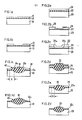
- a substrate 10 of semiconductor material i.e., for example silicon
- oxide layer 12 is formed by thermal oxidation of the substrate 10.
- a layer of silicon nitride 14 is formed over the oxide 12.
- Selective nitride etching is then undertaken to expose a portion of the oxide 12 (Fig. lb), such etching taking place, for example, in accordance with U.S. Patent No. 3,913,211.
- the resulting structure is then placed in an oxidizing environment at an elevated temperature.
- the oxygen in the environment combines with the silicon from silicon substrate 10 to form a thick region of oxidized semiconductor material i.e., insulation region or field oxide 16 (Fig. lc).
- the nitride 14 is then etched, resulting in the structure shown in Fig. ld. Remaining steps as shown in U.S. Patent No. 3,913,211 can be undertaken to complete the semiconductor device.
- the thick field oxide 16 gradually tapers down into the oxide portion 12a. While this provides certain advantages, it will be understood that in certain applications, it is desirable to retain appropriate field oxide characteristics while increasing such taper so that active areas of adjacent semiconductor devices can be positioned more closely together.
- a silicon substrate 20 is provided with a thin layer of oxide 22 thereon, with a layer of silicon nitride 24 on the thin layer of oxide 22 (Fig. 2a).
- the nitride 24 is etched as previously described to act as a mask over the oxide 22, defining an opening exposing a portion of the oxide 22.
- a thin layer of polysilicon 28 is deposited over the structure (Fig. 2b).
- the resulting structure is then oxidized to grow the insulation region 30 (Figs. 2c and 2d).
- the oxide is then etched to provide the structure of Fig. 2e, and the nitride 24 is subsequently etched to provide the structure as shown in Fig. 2f.
- the prior art method also has the problem that, upon growth of the field oxide 16 (Fig. lc), oxinitride can under certain conditions form in the area 40, due to oxygen interacting with not only the substrate 10 but also with the nitride 14. As is well known, this oxinitride remains in place upon etching of the nitride layer 14, causing the gate oxide subsequently grown in the area 40 to grow at a less rapid rate than adjacent thereto. The present method avoids this problem since the nitride 24 is not exposed directly to oxygen during field oxide growth, as in the previous method.
Landscapes
- Internal Circuitry In Semiconductor Integrated Circuit Devices (AREA)
- Local Oxidation Of Silicon (AREA)
- Element Separation (AREA)
- Formation Of Insulating Films (AREA)
Applications Claiming Priority (2)
| Application Number | Priority Date | Filing Date | Title |
|---|---|---|---|
| US26676781A | 1981-05-26 | 1981-05-26 | |
| US266767 | 1988-11-03 |
Publications (2)
| Publication Number | Publication Date |
|---|---|
| EP0067738A2 true EP0067738A2 (fr) | 1982-12-22 |
| EP0067738A3 EP0067738A3 (fr) | 1986-06-11 |
Family
ID=23015923
Family Applications (1)
| Application Number | Title | Priority Date | Filing Date |
|---|---|---|---|
| EP82400922A Withdrawn EP0067738A3 (fr) | 1981-05-26 | 1982-05-18 | Procédé pour réduire les régions débordantes pour dispositif semiconducteur |
Country Status (2)
| Country | Link |
|---|---|
| EP (1) | EP0067738A3 (fr) |
| JP (1) | JPS589343A (fr) |
Cited By (4)
| Publication number | Priority date | Publication date | Assignee | Title |
|---|---|---|---|---|
| GB2198882A (en) * | 1986-12-17 | 1988-06-22 | Samsung Semiconductor Tele | A method of semiconductor device isolation by lateral separation |
| US4818235A (en) * | 1987-02-10 | 1989-04-04 | Industry Technology Research Institute | Isolation structures for integrated circuits |
| GB2252201A (en) * | 1991-01-22 | 1992-07-29 | Samsung Electronics Co Ltd | Method of forming an insulating region in a semiconductor device |
| CN116313789A (zh) * | 2023-02-21 | 2023-06-23 | 上海华虹宏力半导体制造有限公司 | 绝缘栅双极晶体管的形成方法 |
Family Cites Families (3)
| Publication number | Priority date | Publication date | Assignee | Title |
|---|---|---|---|---|
| US3911168A (en) * | 1973-06-01 | 1975-10-07 | Fairchild Camera Instr Co | Method for forming a continuous layer of silicon dioxide over a substrate |
| JPS5197385A (en) * | 1975-02-21 | 1976-08-26 | Handotaisochino seizohoho | |
| JPS55153342A (en) * | 1979-05-18 | 1980-11-29 | Fujitsu Ltd | Semiconductor device and its manufacture |
-
1982
- 1982-05-18 EP EP82400922A patent/EP0067738A3/fr not_active Withdrawn
- 1982-05-26 JP JP57088137A patent/JPS589343A/ja active Pending
Cited By (6)
| Publication number | Priority date | Publication date | Assignee | Title |
|---|---|---|---|---|
| GB2198882A (en) * | 1986-12-17 | 1988-06-22 | Samsung Semiconductor Tele | A method of semiconductor device isolation by lateral separation |
| US4818235A (en) * | 1987-02-10 | 1989-04-04 | Industry Technology Research Institute | Isolation structures for integrated circuits |
| GB2252201A (en) * | 1991-01-22 | 1992-07-29 | Samsung Electronics Co Ltd | Method of forming an insulating region in a semiconductor device |
| DE4129665A1 (de) * | 1991-01-22 | 1992-07-30 | Samsung Electronics Co Ltd | Verfahren zur herstellung eines bauteilisolationsbereiches in einem halbleiterbauelement |
| CN116313789A (zh) * | 2023-02-21 | 2023-06-23 | 上海华虹宏力半导体制造有限公司 | 绝缘栅双极晶体管的形成方法 |
| CN116313789B (zh) * | 2023-02-21 | 2025-10-17 | 上海华虹宏力半导体制造有限公司 | 绝缘栅双极晶体管的形成方法 |
Also Published As
| Publication number | Publication date |
|---|---|
| EP0067738A3 (fr) | 1986-06-11 |
| JPS589343A (ja) | 1983-01-19 |
Similar Documents
| Publication | Publication Date | Title |
|---|---|---|
| US4551910A (en) | MOS Isolation processing | |
| US3913211A (en) | Method of MOS transistor manufacture | |
| KR950001151B1 (ko) | 반도체 장치 제조방법 | |
| US5326715A (en) | Method for forming a field oxide film of a semiconductor device | |
| GB1175603A (en) | Semiconductor Device and Method of Making the Same | |
| JPH0521450A (ja) | 半導体装置及びその製造方法 | |
| US5972777A (en) | Method of forming isolation by nitrogen implant to reduce bird's beak | |
| EP0067738A2 (fr) | Procédé pour réduire les régions débordantes pour dispositif semiconducteur | |
| US5115296A (en) | Preferential oxidization self-aligned contact technology | |
| US4722912A (en) | Method of forming a semiconductor structure | |
| US4766093A (en) | Chemically formed self-aligned structure and wave guide | |
| EP0120614B1 (fr) | Procédé pour la fabrication d'un dispositif semi-conducteur comportant des régions d'isolation | |
| EP0293979A2 (fr) | Structure d'oxyde isolant sans bird-beak pour circuits intégrés | |
| EP0233791A2 (fr) | Transistor à effet de champ à porte isolée et sa méthode de fabrication | |
| JPS59189677A (ja) | 半導体装置の製造方法 | |
| US5506440A (en) | Poly-buffered LOCOS process | |
| US5215935A (en) | Method of forming isolation region in semiconductor device | |
| JPS6310896B2 (fr) | ||
| KR960000373B1 (ko) | 반도체 표면의 단차 형성방법 | |
| JPS6161268B2 (fr) | ||
| KR940001254B1 (ko) | 폴리실리콘을 이용한 반도체 소자의 분리(isolation) 방법 | |
| JP2533141B2 (ja) | 半導体装置の製造方法 | |
| JPH0290569A (ja) | 半導体装置の製造方法 | |
| KR0139890B1 (ko) | 반도체 소자의 필드 산화막 제조방법 | |
| JPS61219148A (ja) | 半導体装置の製造方法 |
Legal Events
| Date | Code | Title | Description |
|---|---|---|---|
| PUAI | Public reference made under article 153(3) epc to a published international application that has entered the european phase |
Free format text: ORIGINAL CODE: 0009012 |
|
| AK | Designated contracting states |
Designated state(s): DE FR GB IT NL |
|
| PUAL | Search report despatched |
Free format text: ORIGINAL CODE: 0009013 |
|
| AK | Designated contracting states |
Kind code of ref document: A3 Designated state(s): DE FR GB IT NL |
|
| STAA | Information on the status of an ep patent application or granted ep patent |
Free format text: STATUS: THE APPLICATION IS DEEMED TO BE WITHDRAWN |
|
| 18D | Application deemed to be withdrawn |
Effective date: 19861212 |
|
| RIN1 | Information on inventor provided before grant (corrected) |
Inventor name: PADMANABHAN, G. R. |