EP0068154A2 - Circuit intégré comportant un substrat semiconducteur ayant des régions d'isolation et des régions électriquement conductrices - Google Patents
Circuit intégré comportant un substrat semiconducteur ayant des régions d'isolation et des régions électriquement conductrices Download PDFInfo
- Publication number
- EP0068154A2 EP0068154A2 EP82104709A EP82104709A EP0068154A2 EP 0068154 A2 EP0068154 A2 EP 0068154A2 EP 82104709 A EP82104709 A EP 82104709A EP 82104709 A EP82104709 A EP 82104709A EP 0068154 A2 EP0068154 A2 EP 0068154A2
- Authority
- EP
- European Patent Office
- Prior art keywords
- layer
- process according
- substrate
- metal
- silicon
- Prior art date
- Legal status (The legal status is an assumption and is not a legal conclusion. Google has not performed a legal analysis and makes no representation as to the accuracy of the status listed.)
- Granted
Links
Images

Classifications
-
- H—ELECTRICITY
- H10—SEMICONDUCTOR DEVICES; ELECTRIC SOLID-STATE DEVICES NOT OTHERWISE PROVIDED FOR
- H10D—INORGANIC ELECTRIC SEMICONDUCTOR DEVICES
- H10D62/00—Semiconductor bodies, or regions thereof, of devices having potential barriers
- H10D62/10—Shapes, relative sizes or dispositions of the regions of the semiconductor bodies; Shapes of the semiconductor bodies
- H10D62/102—Constructional design considerations for preventing surface leakage or controlling electric field concentration
- H10D62/112—Constructional design considerations for preventing surface leakage or controlling electric field concentration for preventing surface leakage due to surface inversion layers, e.g. by using channel stoppers
-
- H—ELECTRICITY
- H10—SEMICONDUCTOR DEVICES; ELECTRIC SOLID-STATE DEVICES NOT OTHERWISE PROVIDED FOR
- H10W—GENERIC PACKAGES, INTERCONNECTIONS, CONNECTORS OR OTHER CONSTRUCTIONAL DETAILS OF DEVICES COVERED BY CLASS H10
- H10W10/00—Isolation regions in semiconductor bodies between components of integrated devices
- H10W10/01—Manufacture or treatment
- H10W10/011—Manufacture or treatment of isolation regions comprising dielectric materials
- H10W10/012—Manufacture or treatment of isolation regions comprising dielectric materials using local oxidation of silicon [LOCOS]
-
- H—ELECTRICITY
- H10—SEMICONDUCTOR DEVICES; ELECTRIC SOLID-STATE DEVICES NOT OTHERWISE PROVIDED FOR
- H10W—GENERIC PACKAGES, INTERCONNECTIONS, CONNECTORS OR OTHER CONSTRUCTIONAL DETAILS OF DEVICES COVERED BY CLASS H10
- H10W10/00—Isolation regions in semiconductor bodies between components of integrated devices
- H10W10/01—Manufacture or treatment
- H10W10/011—Manufacture or treatment of isolation regions comprising dielectric materials
- H10W10/014—Manufacture or treatment of isolation regions comprising dielectric materials using trench refilling with dielectric materials, e.g. shallow trench isolations
- H10W10/0148—Manufacture or treatment of isolation regions comprising dielectric materials using trench refilling with dielectric materials, e.g. shallow trench isolations comprising introducing impurities in side walls or bottom walls of trenches, e.g. for forming channel stoppers
-
- H—ELECTRICITY
- H10—SEMICONDUCTOR DEVICES; ELECTRIC SOLID-STATE DEVICES NOT OTHERWISE PROVIDED FOR
- H10W—GENERIC PACKAGES, INTERCONNECTIONS, CONNECTORS OR OTHER CONSTRUCTIONAL DETAILS OF DEVICES COVERED BY CLASS H10
- H10W10/00—Isolation regions in semiconductor bodies between components of integrated devices
- H10W10/10—Isolation regions comprising dielectric materials
- H10W10/13—Isolation regions comprising dielectric materials formed using local oxidation of silicon [LOCOS], e.g. sealed interface localised oxidation [SILO] or side-wall mask isolation [SWAMI]
-
- H—ELECTRICITY
- H10—SEMICONDUCTOR DEVICES; ELECTRIC SOLID-STATE DEVICES NOT OTHERWISE PROVIDED FOR
- H10W—GENERIC PACKAGES, INTERCONNECTIONS, CONNECTORS OR OTHER CONSTRUCTIONAL DETAILS OF DEVICES COVERED BY CLASS H10
- H10W10/00—Isolation regions in semiconductor bodies between components of integrated devices
- H10W10/10—Isolation regions comprising dielectric materials
- H10W10/17—Isolation regions comprising dielectric materials formed using trench refilling with dielectric materials, e.g. shallow trench isolations
-
- H—ELECTRICITY
- H10—SEMICONDUCTOR DEVICES; ELECTRIC SOLID-STATE DEVICES NOT OTHERWISE PROVIDED FOR
- H10W—GENERIC PACKAGES, INTERCONNECTIONS, CONNECTORS OR OTHER CONSTRUCTIONAL DETAILS OF DEVICES COVERED BY CLASS H10
- H10W20/00—Interconnections in chips, wafers or substrates
- H10W20/01—Manufacture or treatment
- H10W20/021—Manufacture or treatment of interconnections within wafers or substrates
-
- H—ELECTRICITY
- H10—SEMICONDUCTOR DEVICES; ELECTRIC SOLID-STATE DEVICES NOT OTHERWISE PROVIDED FOR
- H10W—GENERIC PACKAGES, INTERCONNECTIONS, CONNECTORS OR OTHER CONSTRUCTIONAL DETAILS OF DEVICES COVERED BY CLASS H10
- H10W20/00—Interconnections in chips, wafers or substrates
- H10W20/20—Interconnections within wafers or substrates, e.g. through-silicon vias [TSV]
Definitions
- the present invention relates to integrated circuits, such as bipolar devices and MOS structures, and to processes for the fabrication thereof.
- Integrated circuits contain a plurality of electrical contacts at preselected locations on the device. Also, a predetermined number of the electrical contacts is in ohmic electrical contact with preselected regions of the substrate in order to provide the semiconductive device.
- the preselected regions include a region which contains ion-implanted or thermally diffused impurities of a second type different from the impurity type of the semiconductor substrate in general.
- the plurality of electrical contacts are the emitter, base, and collector, all of which are in ohmic electrical contact with impurity regions of the device.
- the emitter and collector are in electrical contact with a first type of impurity, while the base is in ohmic electrical contact with a second type of impurity.
- the plurality of electrical contacts include a source, a drain, and a gate, whereby the source and drain are in electrical contact with a region containing a second type of impurity, and whereas the gate is not in ohmic contact with the substrate.
- bipolar devices One particular problem existent in bipolar devices is the resistance in sublayer sheets, such as resistance in the field regions between the emitter and collector contacts.
- the sheet resistance in the sublayers is usually at least about 10 ohm/sq.
- heavily doped buried sublayers, usually called subcollector layers have been used.
- the collector contact is generally located extremely close to the emitter contact. However, this is an important layout constraint in bipolar circuit design.
- the circuits built with them are known to be sensitive to the effect of alpha particles. It is known that if a p-epitaxial substrate on an n type wafer is used instead of a p-type wafer, sensitivity to the effect of alpha particles is greatly reduced, since the n +- type wafer is an effective sink for the electrons generated by the alpha particles.
- the p-epitaxial substrate has to be thin, as compared to the penetration depth of alpha particles, which is about 25 microns. Such a thin and lightly doped (e.g.
- epitaxial layer typically greater than about 10 ohm-cm epitaxial layer has a very high sheet resistance which causes transient local fluctuation of the p-type substrate potential.
- One way to correct for this is to provide a substrate contact to every device or to every few devices. In the conventional contact methods, such a procedure consumes a large amount of the silicon chip area and is, therefore, disadvantageous.
- the present invention provides for significantly reduced sublayer sheet resistance in integrated circuits.
- the present invention also provides for substrate contact to every device in a self-aligned manner without consuming additional substrate chip area. Accordingly, the problem of substrate potential fluctuation discussed hereinabove is overcome by the present invention.
- the present invention makes it possible to remotely locate the collector region with respect to the emitter region and, thereby, improve the layout and wirabilityjof the circuit. For instance, in the case of Integrated Injection Logic, or Merged Transistor Logic arrays in the Weinberger image, the greatly reduced emitter sublayer series resistance will allow proportionately more vertical wiring channels to be used without providing multiple emitter sublayer contact per gate. This, in turn, greatly improves the circuit density and wirability thereof.
- the present invention is concerned with an integrated circuit which contains a semiconductive substrate having field isolation regions and having electrical conductive regions of active impurity dopants.
- the device contains a refractory metallic silicide located beneath the field isolation regions and in electrical contact with electrical conductive regions of active impurity dopants in the substrate.
- the presence of the silicide layer in the required location of the present invention results in greatly reduced sublayer sheet resistance in those regions where it is present. Also, this reduction in the sublayer sheet resistance makes it possible to reduce the dopant concentration in the sublayer. This reduction in sublayer doping concentration, in turn, can result in reduced defect density associated with the sublayer and in a reduction of the sublayer thickness. The reduction of the sublayer thickness would likewise result in a reduction of the depth of the deep isolation trenches in the circuits.
- the process of the present invention is concerned with fabricating the above-defined integrated circuits. Moreover, the preferred process aspects do not require any additional masking steps and yet provide for a self-aligned silicide sublayer.
- the sublayer is self-aligned with respect to the electrical conductive regions to which it is electrically connected.
- the process includes providing a semiconductive substrate of a first conductive type containing active impurities of a first conductive type and then thermally diffusing or ion-implanting active impurities either of the first conductive type or of a second and opposite conductive type into predetermined regions of the semiconductive substrate.
- a refractory metal is deposited at and in electrical connection with these predetermined regions of the semiconductive substrate.
- the metal is then reacted with the substrate beneath the metal in order to form a layer of an electrically conductive refractory compound.
- An insulating layer is then provided above the layer of the electrically conductive refractory compound.
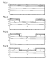
- FIGURE 1.1 to 1.9 are schematic side views of various stages of fabrication of an integrated circuit according to the present invention in the form of a bipolar transistor.
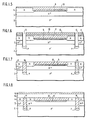
- FIGURE 2.1 and 2.2 are schematic side views of various stages of fabrication of an integrated circuit in the form of a MOSFET or a MOS dynamic RAM DEVICE.
- n-type substrate and p-type diffused or implanted dopant impurities can be employed just as well. It is also to be understood that when the discussion refers to n-type impurities, the process steps are applicable to p-type impurities and vice versa. Also, the present invention is applicable to substrates other than silicon which are known in the art.
- the terms "metallic type interconnection lines" or “high-conductivity interconnection lines” refer to metal lines such as aluminum, as well as to nonmetallic materials (e.g.
- fabrication steps refers to photolithography.
- other lithographic techniques such as electron beam systems, can be employed when desired.
- the discussion which follows employs the preferred material, polycrystalline silicon, as, for instance, a gate material
- other materials can be employed to provide various conductive layers, such as the gates.
- such can be fabricated from a refractory metal or silicide thereof.
- a refractory metal as will be discussed herein, is understood within the context of the present invention to be a metal which can withstand the high temperatures experienced during the fabrication without degrading to an undesired extent. Examples of some refractory metals include tungsten, tantalum, hafnium, molybdenum, vanadium, niobium, rhodium, and cobalt.
- a p-type silicon substrate 2 having any desired crystal orientation which can be prepared by slicing and polishing a p-type silicon boule grown in the presence of a p-type dopant, such as boron, following conventional crystal growth techniques.
- a p-type dopant such as boron
- Other p-dopants for silicon include aluminium gallium, and indium.
- a typical dosage of the p-type dopants is about 1 0 15 atoms/cm 3 .
- n-type impurity sublayer 3 Located on the p-substrate is a n-type impurity sublayer 3 containing an enhanced concentration of n-type dopant impurities, such as phosphorus, arsenic, or antimony usually present in a concentration of about 10 20 atoms/cm 3 .
- n-epitaxially grown silicon layer 4 Located on top of the n + sublayer 3 is a n-epitaxially grown silicon layer 4 containing n-type impurities, such as phosphorus, arsenic, or antimony.
- a typical concentration of the n-type impurities is about 1 0 16 atoms/cm 3 .
- An adherent oxidation barrier layer 6 or a nonoxidizing material, such as silicon nitride, aluminum nitride, boron nitride, alumi.niumoxide, or silicon carbide is then deposited.
- the layer 6 is a nitride such as silicon nitride and is approximately 500 to 0 about 3000 A thick.
- the layer 6 may be deposited by conventional chemical-vapour deposition techniques.
- An additional layer of silicon dioxide 7 is then deposited.
- the silicon dioxide layer 7 is approximately 100 to 0 about 1000 A thick and may be formed by chemical-vapour deposition.
- the oxidation barrier layer material should not oxidize, or at most only oxidize extremely slowly relative to the oxidation rate of silicon and polycrystalline silicon.
- the oxidation barrier layer material is considered to be a nonoxidizing material under the conditions to which it is subjected in the method of the present invention.
- a pattern-determining layer such as a layer of resist material (not shown) of the type employed in known lithographic masking and etching techniques is placed over the surface of the upper oxide layer 7. Any of the well-known photosensitive polymerizable resist materials known in the art may be used.
- the resist material is applied, such as by spinning on or by spraying.
- the layer of photoresist material is dried and then selectively exposed to ultraviolet radiation using a photolithographic mask.
- the mask is of a transparent material having opaque portions in a predetermined pattern.
- the masked wafer is subject to ultraviolet light which polymerizes the portions of the resist material underlying the transparent regions of the mask.
- the wafer is rinsed in a suitable developing solution which washes away the portions of the resist material which were not under the opaque portions of the mask and, thus, exposed to the ultraviolet light.
- the structure is treated to remove the portions of the silicon dioxide layers 5 and 7 and the silicon nitride layer 6 not protected by the resist material
- the portions removed of such layers are regions wherein recessed field oxide is to be subsequently formed.
- the silicon dioxide and silicon nitride layer can be removed by standard wet chemical etching or by reactive ion etching, such as using CF 4 plus hydrogen.
- a portion of the epitaxial silicon is removed by reactive ion etching, such as using CF 4 or CC1 2 CF 2 plus oxygen, in those regions wherein recessed field oxide is subsequently formed. Approxi- ° mately 2000 A to about 1 micron, and most preferably about one-half micron, of the n-epitaxial silicon layer is removed.
- the n-epitaxial silicon layer 4 initially is about 0.5 micron to about 2 microns, and preferably about 1 micron.
- a layer of silicon dioxide 8 is thermally grown 0 (Fig. 1.3). Such is approximately 1000 A to about 1 micron thick, and preferably about 2000 A. It can be grown by thermal oxidation of the assembly at about 1000°C in the presence of dry oxygen. If desired, this oxide layer can be provided by a combination of thermally grown silicon dioxide and chemical vapourdeposited dioxide.
- the silicon dioxide layer is removed by reactive ion etching employing, for instance, a gaseous fluorocarbon, such as CF 4 and H 2 supplying gas in order to provide selective etching of the silicon dioxide as opposed to etching of the silicon beneath the oxide layer.
- a gaseous fluorocarbon such as CF 4 and H 2 supplying gas in order to provide selective etching of the silicon dioxide as opposed to etching of the silicon beneath the oxide layer.
- the reactive ion etching removes all of the exposed silicon dioxide layer except for that silicon dioxide on the side wall on the silicon as shown in Fig. 1.3.
- a discussion on using reactive ion etching to remove silicon dioxide everywhere except on vertical sidewalls can be found in U .S. 4,234,362.
- an n-type dopant is introduced such as by ion-implantation, to provide enhanced doping in the recessed region.
- An example of an n-type dopant is an arsenic implant of about 100 to about 300 keV energy and about 10 15 atoms/cm 2 dose and resulting in a 10 20 atom/cm 3 concentration.
- a refractory metal is then deposited, such as by sputtering or preferably by evaporation.
- suitable refractory metals include tungsten, tantalum, niobium, molybdenum, hafnium, cobalt, and vanadium, and preferably tungsten and tantalum. Mixtures can be employed if desired.
- the electrically conductive compound of the refractory metal 9 is formed by reacting the metal with the substrate (Fig. 1.4). In the case of silicon, the compound formed is a silicide.
- the compound or silicide can be formed by either reacting the metal at elevated temperatures, such as at about 700°C to about 1100°C, or by implanting certain ions through the metal layer, such as inert gas ions, such as argon, krypton, and xenon, or other ions, such as antimony or silicon.
- elevated temperatures such as at about 700°C to about 1100°C
- ions such as inert gas ions, such as argon, krypton, and xenon, or other ions, such as antimony or silicon.
- the silicon nitride layer 6 prevents refractory metal located above it from reacting with any silicon.
- the metal which does not react is then removed by dissolving in a suitable composition.
- tantalum can be removed by employing a KOH solution.
- the thickness of the metal layer is usually about 500 A to about 2000 A.
- Recess oxide 10 (Fig. 1.5) is next formed by thermal oxidation at about 800 to about 1000°C in dry oxygen. During oxidation, silicon diffuses upward through the silicide layer to form the oxide. Next, the oxidation mask, silicon nitride 6, is removed by employing a suitable etchant which does not attack the oxide present or other components of the already formed device. For instance, silicon nitride can be removed by phosphoric acid solution at about 180°C.
- the recessed oxide layer can be formed by depositing, such as by chemical vapour deposition, a layer of silicon oxide and then planarizing the surface with a photoresist and then etching back by use of reactive ion etching, such as in CF 4 or mixture of CF 4 and H 2 as discussed hereinabove.
- deep dielectric or deep trench isolation is next formed.
- One convenient way to do such is to deposit a layer of polysilicon 11 -- (Fig. 1.6).
- the polysilicon layer is approximately 1500 to about 5000 A thick and may be formed by chemical vapour deposition.
- a silicon dioxide layer 12 is formed over the polysilicon layer 11.
- the silicon dioxide layer 12 is ° about 1500 to about 5000 A thick and can be formed by chemical vapourdeposition.
- the polysilicon layer 12 serves as a reactive ion etching stop when silicon dioxide is to be etched.
- a photoresist mask (nQt shown) is applied to the assembly and preselected portions thereof are removed by use of a photolithographic mask. Those portions not protected by the photoresist are removed by reactive ion etching.
- the silicon dioxide is etched by reactive ion etching employing CF 4 and H 2 , as discussed hereinabove.
- the polysilicon and silicon are etched by employing C1 2 plus Ar, CF 4 , or CC1 2 F 2 plus 0 2 .
- the trenches 13 in the silicon are removed by selective reactive ion etching in Cl 2 plus Ar or CCl 2 F 2 plus 0 2 .
- channel stops are formed in the bottoms of the trench by ion implantation of a p-type dopant.
- a thin layer of silicon dioxide (not shown) of about 0 200 to about 1000 A thick is grown on the exposed silicon surface.
- silicon dioxide 14 (Fig. 1.7) is chemically vapour deposited to fill up the trenches.
- the surface is then planarized using a photoresist and etching process. All of the photoresist can be removed by reactive ion etching in CF 4 .
- the silicon oxide on top of the polysilicon is removed by reactive ion etching in CF 4 and hydrogen as discussed hereinabove.
- the polysilicon layer is removed, for instance, by etching in a solution of pyrocatechol.
- the silicon oxide layer is removed from those areas on top of the active device regions.
- the deep trench isolation process is thus complete and the refractory metal silicide layer 9 is in place.
- the usual process steps can be followed to fabricate the desired bipolar device and circuit.
- the following fabrication steps are merely presented as illustrative of the procedure that can be employed to form an npn bipolar transistor having its emitter self-aligned to its polysilicon base contact.
- a discussion of such self-alignment bipolar transistors can be found in U.S. 4,157,269 and EP-0005721 - and in Ning et al, "Self-Aligned NPN Bipolar Transistors", 1980, International Electron Devices Meeting Technical Digest, pp. 823-824.
- a layer 15 of polycrystalline silicon is then deposited (Fig. 1.8).
- the polycrystalline silicon is approxi-0 mately 1500 to 5000 A thick, and may be formed by chemical-vapour deposition.
- Layer 16 of silicon dioxide is then deposited.
- the silicon dioxide layer 16 is 0 approximately 2000 to 5000 A thick and may be formed by chemical vapourdeposition.
- a pattern determining layer (not shown), such as a layer of resist material of the type employed in known lithographic masking and etching techniques, is placed over the entire surface of the upper oxide 16. Any of the well-known polymerizable resist materials known in the art may be used.
- the resist material is applied, such as by spinning on or by spraying.
- the layer of photoresist material is dried and then selectively exposed to ultraviolet radiation using a photolithographic mask.
- the silicon dioxide 16 is reactive ion etched in CF 4 and H 2
- the polysilicon layer 15 is partially reactive ion etched in CF 4 .
- a thin silicon dioxide layer is then formed on the exposed silicon and polysilicon surfaces by thermal oxidation. This 0 layer is approximately 100 to about 1000 A thick. Another layer of silicon dioxide approximately 1000 to 0 about 3000 A thick is then put down by chemical vapour deposition. This combined layer of thermal silicon dioxide and chemical-vapor deposited-silicon dioxide is then reactive ion etched in CF 4 and H 2 , removing it everywhere except on the sidewalls of polysilicon layer 15. Thus, the polysilicon layer is insulated on the top by silicon dioxide 16 and on the vertical sides by silicon dioxide 19 (Fig. 1.9).
- N-type impurities such as arsenic
- P-type impurities such as boron
- the polysilicon layer 15 and the silicon dioxide 19 together act as the mask in the emitter and intrinsic base formation process.
- the emitter region is self-aligned to the polysilicon 15 which contacts the base region.
- any integrated circuit it is necessary to connect high-electrical conductivity lines to the various active elements of the device.
- the electrical connections are fabricated by applying a photoresist layer (not shown) to the assembly.
- the resist is exposed to ultraviolet radiation using a lithographic masking pattern, and the exposed regions of the resist are dissolved away.
- the structure is treated to remove the portions of the silicon dioxide not protected by the resist material. For instance, the wafer is immersed in a solution of buffered hydrofluoric acid to provide contact holes or vias through the oxide layer to allow electrical connection to be made.
- the remaining photoresist above the etched silicon dioxide is then removed by dissolving a suitable solvent.
- the metallic type higher electrical conductivity interconnection line material 20 preferably a metal
- the interconnection pattern is delineated.
- An example of a highly conductive material commonly used for interconnection is aluminium.
- the high-electrical conductivity material, such as aluminium, may be deposited by sputtering or, preferably, by evaporation.
- a photoresist layer (not shown) is applied to the assembly.
- the resist material is exposed with ultraviolet radiation using a predetermined mask pattern.
- the structure is treated to remove portions of the conductive material not protected by the resist.
- the resist material over the pattern conductive material is removed by dissolving in suitable solvent.
- FIG. 2.1 illustrates a partially fabricated MOSFET which is achieved by the same sequence steps as is the structure shown in Fig. 1.5, except that the starting substrate is a p-epitaxially grown silicon substrate 21 on an n silicon wafer 22 and the implantation is p-type whereas the process discussed with respect to Fig. 1 employs n-type.
- a device along the lines of Fig. 2.2 can be prepared by employing conventional or known processing techniques.
- numeral 23 represents n source and/or drain regions
- 24 represents silicon dioxide isolation areas
- 25, 26 and 27 represent polycrystalline silicon gates
- 28 represents metallic interconnections.
- gates 26 and 27 can be formed by self-aligning technique as described in U.S. 4282540 and EP-0002997.
Landscapes
- Bipolar Transistors (AREA)
- Electrodes Of Semiconductors (AREA)
- Element Separation (AREA)
- Internal Circuitry In Semiconductor Integrated Circuit Devices (AREA)
- Semiconductor Memories (AREA)
Applications Claiming Priority (2)
| Application Number | Priority Date | Filing Date | Title |
|---|---|---|---|
| US279119 | 1981-06-30 | ||
| US06/279,119 US4446476A (en) | 1981-06-30 | 1981-06-30 | Integrated circuit having a sublayer electrical contact and fabrication thereof |
Publications (3)
| Publication Number | Publication Date |
|---|---|
| EP0068154A2 true EP0068154A2 (fr) | 1983-01-05 |
| EP0068154A3 EP0068154A3 (en) | 1986-05-07 |
| EP0068154B1 EP0068154B1 (fr) | 1989-03-08 |
Family
ID=23067705
Family Applications (1)
| Application Number | Title | Priority Date | Filing Date |
|---|---|---|---|
| EP82104709A Expired EP0068154B1 (fr) | 1981-06-30 | 1982-05-28 | Circuit intégré comportant un substrat semiconducteur ayant des régions d'isolation et des régions électriquement conductrices |
Country Status (4)
| Country | Link |
|---|---|
| US (1) | US4446476A (fr) |
| EP (1) | EP0068154B1 (fr) |
| JP (1) | JPS587840A (fr) |
| DE (1) | DE3279523D1 (fr) |
Cited By (4)
| Publication number | Priority date | Publication date | Assignee | Title |
|---|---|---|---|---|
| US4450620A (en) * | 1983-02-18 | 1984-05-29 | Bell Telephone Laboratories, Incorporated | Fabrication of MOS integrated circuit devices |
| EP0127142A1 (fr) * | 1983-05-24 | 1984-12-05 | Kabushiki Kaisha Toshiba | Dispositif à semi-conducteurs avec au moins un transistor à effet de champ |
| US4851359A (en) * | 1985-12-27 | 1989-07-25 | Bull S.A. | Method of producing an electrical resistor by implanting a semiconductor material with rare gas |
| EP1794806A4 (fr) * | 2004-09-21 | 2011-06-29 | Ibm | Procede de formation de collecteur dans la technologie bicmos |
Families Citing this family (24)
| Publication number | Priority date | Publication date | Assignee | Title |
|---|---|---|---|---|
| GB2118363A (en) * | 1982-04-08 | 1983-10-26 | Philips Electronic Associated | Hot-electron and hot-hole transistors |
| US4982244A (en) * | 1982-12-20 | 1991-01-01 | National Semiconductor Corporation | Buried Schottky clamped transistor |
| US4688069A (en) * | 1984-03-22 | 1987-08-18 | International Business Machines Corporation | Isolation for high density integrated circuits |
| US4829363A (en) * | 1984-04-13 | 1989-05-09 | Fairchild Camera And Instrument Corp. | Structure for inhibiting dopant out-diffusion |
| US4589193A (en) * | 1984-06-29 | 1986-05-20 | International Business Machines Corporation | Metal silicide channel stoppers for integrated circuits and method for making the same |
| US4597163A (en) * | 1984-12-21 | 1986-07-01 | Zilog, Inc. | Method of improving film adhesion between metallic silicide and polysilicon in thin film integrated circuit structures |
| US4745081A (en) * | 1985-10-31 | 1988-05-17 | International Business Machines Corporation | Method of trench filling |
| US4728626A (en) * | 1985-11-18 | 1988-03-01 | International Business Machines Corporation | Method for making planar 3D heterepitaxial semiconductor structures with buried epitaxial silicides |
| US4711017A (en) * | 1986-03-03 | 1987-12-08 | Trw Inc. | Formation of buried diffusion devices |
| US4933295A (en) * | 1987-05-08 | 1990-06-12 | Raytheon Company | Method of forming a bipolar transistor having closely spaced device regions |
| US4902533A (en) * | 1987-06-19 | 1990-02-20 | Motorola, Inc. | Method for selectively depositing tungsten on a substrate by using a spin-on metal oxide |
| JPH021988A (ja) * | 1987-12-03 | 1990-01-08 | Texas Instr Inc <Ti> | 電気的にプログラム可能なメモリ・セル |
| US5023200A (en) * | 1988-11-22 | 1991-06-11 | The United States Of America As Represented By The United States Department Of Energy | Formation of multiple levels of porous silicon for buried insulators and conductors in silicon device technologies |
| US5097312A (en) * | 1989-02-16 | 1992-03-17 | Texas Instruments Incorporated | Heterojunction bipolar transistor and integration of same with field effect device |
| US5180432A (en) * | 1990-01-08 | 1993-01-19 | Lsi Logic Corporation | Apparatus for conducting a refractory metal deposition process |
| DE69033760T2 (de) * | 1990-01-08 | 2001-10-25 | Lsi Logic Corp | Struktur zum Filtern von Prozessgasen zum Einsatz in einer Kammer für chemische Dampfabscheidung |
| US5027183A (en) * | 1990-04-20 | 1991-06-25 | International Business Machines | Isolated semiconductor macro circuit |
| JP2895166B2 (ja) * | 1990-05-31 | 1999-05-24 | キヤノン株式会社 | 半導体装置の製造方法 |
| US5604159A (en) * | 1994-01-31 | 1997-02-18 | Motorola, Inc. | Method of making a contact structure |
| DE19638438A1 (de) * | 1996-09-19 | 1998-04-02 | Siemens Ag | Durch Feldeffekt steuerbares, vertikales Halbleiterbauelement |
| JP2001352079A (ja) * | 2000-06-07 | 2001-12-21 | Nec Corp | ダイオードおよびその製造方法 |
| US6515488B1 (en) * | 2001-05-07 | 2003-02-04 | Stmicroelectronics, Inc. | Fingerprint detector with scratch resistant surface and embedded ESD protection grid |
| US7911022B2 (en) * | 2005-01-12 | 2011-03-22 | Taiwan Semiconductor Manufacturing Co., Ltd. | Isolation structure in field device |
| US7863709B1 (en) * | 2007-04-16 | 2011-01-04 | Marvell International Ltd. | Low base resistance bipolar junction transistor array |
Family Cites Families (12)
| Publication number | Priority date | Publication date | Assignee | Title |
|---|---|---|---|---|
| NL144775B (nl) * | 1964-09-23 | 1975-01-15 | Philips Nv | Halfgeleiderinrichting met meer dan een halfgeleiderschakelelement in een lichaam. |
| US3381182A (en) * | 1964-10-19 | 1968-04-30 | Philco Ford Corp | Microcircuits having buried conductive layers |
| US3659162A (en) * | 1968-12-27 | 1972-04-25 | Nippon Electric Co | Semiconductor integrated circuit device having improved wiring layer structure |
| US3653120A (en) * | 1970-07-27 | 1972-04-04 | Gen Electric | Method of making low resistance polycrystalline silicon contacts to buried collector regions using refractory metal silicides |
| US3748187A (en) * | 1971-08-03 | 1973-07-24 | Hughes Aircraft Co | Self-registered doped layer for preventing field inversion in mis circuits |
| BE792001A (fr) * | 1971-11-29 | 1973-03-16 | Western Electric Co | Structures a circuits integres a croisements |
| US3908187A (en) * | 1973-01-02 | 1975-09-23 | Gen Electric | High voltage power transistor and method for making |
| US4005452A (en) * | 1974-11-15 | 1977-01-25 | International Telephone And Telegraph Corporation | Method for providing electrical isolating material in selected regions of a semiconductive material and the product produced thereby |
| US4128670A (en) * | 1977-11-11 | 1978-12-05 | International Business Machines Corporation | Fabrication method for integrated circuits with polysilicon lines having low sheet resistance |
| US4157269A (en) * | 1978-06-06 | 1979-06-05 | International Business Machines Corporation | Utilizing polysilicon diffusion sources and special masking techniques |
| US4234362A (en) * | 1978-11-03 | 1980-11-18 | International Business Machines Corporation | Method for forming an insulator between layers of conductive material |
| JPS5669844A (en) * | 1979-11-10 | 1981-06-11 | Toshiba Corp | Manufacture of semiconductor device |
-
1981
- 1981-06-30 US US06/279,119 patent/US4446476A/en not_active Expired - Lifetime
-
1982
- 1982-04-20 JP JP57064848A patent/JPS587840A/ja active Pending
- 1982-05-28 DE DE8282104709T patent/DE3279523D1/de not_active Expired
- 1982-05-28 EP EP82104709A patent/EP0068154B1/fr not_active Expired
Cited By (4)
| Publication number | Priority date | Publication date | Assignee | Title |
|---|---|---|---|---|
| US4450620A (en) * | 1983-02-18 | 1984-05-29 | Bell Telephone Laboratories, Incorporated | Fabrication of MOS integrated circuit devices |
| EP0127142A1 (fr) * | 1983-05-24 | 1984-12-05 | Kabushiki Kaisha Toshiba | Dispositif à semi-conducteurs avec au moins un transistor à effet de champ |
| US4851359A (en) * | 1985-12-27 | 1989-07-25 | Bull S.A. | Method of producing an electrical resistor by implanting a semiconductor material with rare gas |
| EP1794806A4 (fr) * | 2004-09-21 | 2011-06-29 | Ibm | Procede de formation de collecteur dans la technologie bicmos |
Also Published As
| Publication number | Publication date |
|---|---|
| EP0068154B1 (fr) | 1989-03-08 |
| DE3279523D1 (en) | 1989-04-13 |
| US4446476A (en) | 1984-05-01 |
| EP0068154A3 (en) | 1986-05-07 |
| JPS587840A (ja) | 1983-01-17 |
Similar Documents
| Publication | Publication Date | Title |
|---|---|---|
| EP0068154B1 (fr) | Circuit intégré comportant un substrat semiconducteur ayant des régions d'isolation et des régions électriquement conductrices | |
| EP0036082B1 (fr) | Procédé autoaligné pour la réalisation d'un transistor bipolaire à haute performance | |
| US4521952A (en) | Method of making integrated circuits using metal silicide contacts | |
| EP0088922B1 (fr) | Procédé pour fabriquer des électrodes et bandes d'interconnexion sur un dispositif semi-conducteur | |
| EP0083089B1 (fr) | Procédé pour la fabrication d'une configuration métallique par auto-alignement pour dispositifs semi-conducteurs | |
| KR100219332B1 (ko) | 게이트 전극 및 소스와 드레인 영역 사이의 단락을 없애는 얕은 불순물 영역을 구비한 반도체 디바이스 및 이를 제조하는 공정 | |
| EP0137905B1 (fr) | Procédé pour la fabrication de transistors bipolaires latéraux | |
| EP0098374A2 (fr) | Structure d'isolation diélectrique pour circuits intégrés et procédé pour la fabrication de cette structure | |
| EP0442718A2 (fr) | Procédé de fabrication d'un dispositif semi-conducteur | |
| EP0126424A2 (fr) | Procédé pour la fabrication des structures en polyciures | |
| US4661832A (en) | Total dielectric isolation for integrated circuits | |
| US4871684A (en) | Self-aligned polysilicon emitter and contact structure for high performance bipolar transistors | |
| EP0076106B1 (fr) | Procédé de fabrication d'un transistor bipolaire | |
| US4824794A (en) | Method for fabricating a bipolar transistor having self aligned base and emitter | |
| JPH0241170B2 (fr) | ||
| US5670417A (en) | Method for fabricating self-aligned semiconductor component | |
| EP0036499B1 (fr) | Procédé auto-aligné pour transistor bipolaire à base en polysilicium | |
| US6774455B2 (en) | Semiconductor device with a collector contact in a depressed well-region | |
| US4956689A (en) | High speed gallium arsenide transistor and method | |
| US6806159B2 (en) | Method for manufacturing a semiconductor device with sinker contact region | |
| US7101750B2 (en) | Semiconductor device for integrated injection logic cell and process for fabricating the same | |
| US5053346A (en) | Method for making a high speed gallium arsenide transistor | |
| US7164186B2 (en) | Structure of semiconductor device with sinker contact region | |
| KR100258438B1 (ko) | 바이폴라 트랜지스터 제조방법 | |
| EP0600693A2 (fr) | Attaque sélective et structure base-émetteur auto-alignée |
Legal Events
| Date | Code | Title | Description |
|---|---|---|---|
| PUAI | Public reference made under article 153(3) epc to a published international application that has entered the european phase |
Free format text: ORIGINAL CODE: 0009012 |
|
| AK | Designated contracting states |
Designated state(s): DE FR GB |
|
| 17P | Request for examination filed |
Effective date: 19830420 |
|
| PUAL | Search report despatched |
Free format text: ORIGINAL CODE: 0009013 |
|
| AK | Designated contracting states |
Kind code of ref document: A3 Designated state(s): DE FR GB |
|
| 17Q | First examination report despatched |
Effective date: 19870907 |
|
| GRAA | (expected) grant |
Free format text: ORIGINAL CODE: 0009210 |
|
| AK | Designated contracting states |
Kind code of ref document: B1 Designated state(s): DE FR GB |
|
| REF | Corresponds to: |
Ref document number: 3279523 Country of ref document: DE Date of ref document: 19890413 |
|
| ET | Fr: translation filed | ||
| PLBE | No opposition filed within time limit |
Free format text: ORIGINAL CODE: 0009261 |
|
| STAA | Information on the status of an ep patent application or granted ep patent |
Free format text: STATUS: NO OPPOSITION FILED WITHIN TIME LIMIT |
|
| 26N | No opposition filed | ||
| PGFP | Annual fee paid to national office [announced via postgrant information from national office to epo] |
Ref country code: FR Payment date: 19910430 Year of fee payment: 10 |
|
| PGFP | Annual fee paid to national office [announced via postgrant information from national office to epo] |
Ref country code: GB Payment date: 19920409 Year of fee payment: 11 |
|
| PGFP | Annual fee paid to national office [announced via postgrant information from national office to epo] |
Ref country code: DE Payment date: 19920523 Year of fee payment: 11 |
|
| PG25 | Lapsed in a contracting state [announced via postgrant information from national office to epo] |
Ref country code: FR Effective date: 19930129 |
|
| REG | Reference to a national code |
Ref country code: FR Ref legal event code: ST |
|
| PG25 | Lapsed in a contracting state [announced via postgrant information from national office to epo] |
Ref country code: GB Effective date: 19930528 |
|
| GBPC | Gb: european patent ceased through non-payment of renewal fee |
Effective date: 19930528 |
|
| PG25 | Lapsed in a contracting state [announced via postgrant information from national office to epo] |
Ref country code: DE Effective date: 19940201 |