EP0068416A2 - Diode électroluminescente à rendement et fréquence limite de modulation élevés - Google Patents
Diode électroluminescente à rendement et fréquence limite de modulation élevés Download PDFInfo
- Publication number
- EP0068416A2 EP0068416A2 EP82105471A EP82105471A EP0068416A2 EP 0068416 A2 EP0068416 A2 EP 0068416A2 EP 82105471 A EP82105471 A EP 82105471A EP 82105471 A EP82105471 A EP 82105471A EP 0068416 A2 EP0068416 A2 EP 0068416A2
- Authority
- EP
- European Patent Office
- Prior art keywords
- layer
- luminescent diode
- diode
- luminescent
- mixed crystal
- Prior art date
- Legal status (The legal status is an assumption and is not a legal conclusion. Google has not performed a legal analysis and makes no representation as to the accuracy of the status listed.)
- Granted
Links
Images

Classifications
-
- H—ELECTRICITY
- H10—SEMICONDUCTOR DEVICES; ELECTRIC SOLID-STATE DEVICES NOT OTHERWISE PROVIDED FOR
- H10P—GENERIC PROCESSES OR APPARATUS FOR THE MANUFACTURE OR TREATMENT OF DEVICES COVERED BY CLASS H10
- H10P14/00—Formation of materials, e.g. in the shape of layers or pillars
- H10P14/20—Formation of materials, e.g. in the shape of layers or pillars of semiconductor materials
- H10P14/34—Deposited materials, e.g. layers
- H10P14/3402—Deposited materials, e.g. layers characterised by the chemical composition
- H10P14/3414—Deposited materials, e.g. layers characterised by the chemical composition being group IIIA-VIA materials
- H10P14/3421—Arsenides
-
- H—ELECTRICITY
- H10—SEMICONDUCTOR DEVICES; ELECTRIC SOLID-STATE DEVICES NOT OTHERWISE PROVIDED FOR
- H10H—INORGANIC LIGHT-EMITTING SEMICONDUCTOR DEVICES HAVING POTENTIAL BARRIERS
- H10H20/00—Individual inorganic light-emitting semiconductor devices having potential barriers, e.g. light-emitting diodes [LED]
- H10H20/01—Manufacture or treatment
- H10H20/011—Manufacture or treatment of bodies, e.g. forming semiconductor layers
- H10H20/013—Manufacture or treatment of bodies, e.g. forming semiconductor layers having light-emitting regions comprising only Group III-V materials
-
- H—ELECTRICITY
- H10—SEMICONDUCTOR DEVICES; ELECTRIC SOLID-STATE DEVICES NOT OTHERWISE PROVIDED FOR
- H10H—INORGANIC LIGHT-EMITTING SEMICONDUCTOR DEVICES HAVING POTENTIAL BARRIERS
- H10H20/00—Individual inorganic light-emitting semiconductor devices having potential barriers, e.g. light-emitting diodes [LED]
- H10H20/80—Constructional details
- H10H20/81—Bodies
- H10H20/811—Bodies having quantum effect structures or superlattices, e.g. tunnel junctions
-
- H—ELECTRICITY
- H10—SEMICONDUCTOR DEVICES; ELECTRIC SOLID-STATE DEVICES NOT OTHERWISE PROVIDED FOR
- H10H—INORGANIC LIGHT-EMITTING SEMICONDUCTOR DEVICES HAVING POTENTIAL BARRIERS
- H10H20/00—Individual inorganic light-emitting semiconductor devices having potential barriers, e.g. light-emitting diodes [LED]
- H10H20/80—Constructional details
- H10H20/81—Bodies
- H10H20/822—Materials of the light-emitting regions
- H10H20/824—Materials of the light-emitting regions comprising only Group III-V materials, e.g. GaP
-
- H—ELECTRICITY
- H10—SEMICONDUCTOR DEVICES; ELECTRIC SOLID-STATE DEVICES NOT OTHERWISE PROVIDED FOR
- H10P—GENERIC PROCESSES OR APPARATUS FOR THE MANUFACTURE OR TREATMENT OF DEVICES COVERED BY CLASS H10
- H10P14/00—Formation of materials, e.g. in the shape of layers or pillars
- H10P14/20—Formation of materials, e.g. in the shape of layers or pillars of semiconductor materials
- H10P14/26—Formation of materials, e.g. in the shape of layers or pillars of semiconductor materials using liquid deposition
- H10P14/263—Formation of materials, e.g. in the shape of layers or pillars of semiconductor materials using liquid deposition using melted materials
-
- H—ELECTRICITY
- H10—SEMICONDUCTOR DEVICES; ELECTRIC SOLID-STATE DEVICES NOT OTHERWISE PROVIDED FOR
- H10P—GENERIC PROCESSES OR APPARATUS FOR THE MANUFACTURE OR TREATMENT OF DEVICES COVERED BY CLASS H10
- H10P14/00—Formation of materials, e.g. in the shape of layers or pillars
- H10P14/20—Formation of materials, e.g. in the shape of layers or pillars of semiconductor materials
- H10P14/26—Formation of materials, e.g. in the shape of layers or pillars of semiconductor materials using liquid deposition
- H10P14/265—Formation of materials, e.g. in the shape of layers or pillars of semiconductor materials using liquid deposition using solutions
-
- H—ELECTRICITY
- H10—SEMICONDUCTOR DEVICES; ELECTRIC SOLID-STATE DEVICES NOT OTHERWISE PROVIDED FOR
- H10P—GENERIC PROCESSES OR APPARATUS FOR THE MANUFACTURE OR TREATMENT OF DEVICES COVERED BY CLASS H10
- H10P14/00—Formation of materials, e.g. in the shape of layers or pillars
- H10P14/20—Formation of materials, e.g. in the shape of layers or pillars of semiconductor materials
- H10P14/29—Formation of materials, e.g. in the shape of layers or pillars of semiconductor materials characterised by the substrates
- H10P14/2901—Materials
- H10P14/2907—Materials being Group IIIA-VA materials
- H10P14/2911—Arsenides
Definitions
- the present invention relates to a luminescent diode as specified in the preamble of claim 1.
- the silicon has an amphoteric doping character, namely as a function of the deposition temperature.
- Luminescent diodes with "graded-band-gap" have a relatively large half-value width of their emission spectrum.
- Luminescent diodes with a single hetero structure and with a double heterostructure.
- Such diodes are manufactured in such a way that they contain at least two epitaxial layers which are produced in two separate epitaxial steps.
- the object of the present invention is to provide a luminescent diode which is suitable for its respective emis sions (frequency) range, preferably in the infrared range and / or in the visible range, has a high electro-optical efficiency and / or which has a high cut-off frequency, in particular of at least 5 MHz, for its modulation and with little technical and technological effort and small rejects can be produced.
- emis sions frequency
- the object of the present invention is to provide a luminescent diode which is suitable for its respective emis sions (frequency) range, preferably in the infrared range and / or in the visible range, has a high electro-optical efficiency and / or which has a high cut-off frequency, in particular of at least 5 MHz, for its modulation and with little technical and technological effort and small rejects can be produced.
- the idea of the present invention is based on the consideration that luminescent diodes which can be produced inexpensively and with only a small amount of rejects can only be obtained by methods in which only a single epitaxy step is necessary.
- multiple epitaxy, as with heterostructures is not only complex, but also leads to deficiency in contamination because the interface in the gas space is exposed when changing from one epitaxial process to the next epitaxial process.
- the invention is based on the finding that, in order to achieve widespread technical use of a new luminescent diode, the wide stop value range of the long-known, silicon-doped luminescent diode with "graded-band-gap" must be reduced.
- luminescent diodes doped according to the principle of the invention with "graded bend gap” have such a high electro-optical efficiency, particularly in the short-wave infrared range and down to the visible red range of the emission that they not only exceed known luminescent diodes with "graded-band-gap", but also those luminescent diodes that are produced using much more complex manufacturing processes.
- the invention also has the further advantage that luminescent diodes constructed according to the principle of the invention have an upper cut-off frequency for the modulation which is in the MHz range and permits modulation bandwidths up to 5 MHz, ie up to the video bandwidth.
- the portion of the mixed crystal epitaxial layer which must have n-type conduction is doped with sulfur or selenium or preferably with tellurium.
- these elements are already made in the melt used in the epitaxy process for producing the layer contain.
- the layer structure of this n-type doping is continued until a solid crystal composition with an aluminum content is epitaxially deposited, which leads to the bandgap which corresponds to the required emission wavelength maximum of the spectral emission range of the diode.
- zinc is added to the melt, from which the epitaxial layer is continuously deposited.
- This zinc element can be added via the gas phase or as a solid.
- the doping effect of the zinc is such that the n-type doping of the dopant still contained in the melt is overcompensated to such an extent that layer portions with p-type conductors now arise.
- Gallium aluminum arsenide is preferably used as the composition of the mixed crystal epitaxial layer for luminescent diodes.
- the use of liquid phase epitaxy is particularly advantageous.
- the combination of tellurium with zinc is preferred, and it is advantageous to add the zinc from the gas phase.
- FIG. 1 denotes a mixed crystal layer made of, for example, gallium aluminum arsenide and produced by epitaxy, the thickness d of which is exaggeratedly large. Actual layer thicknesses of finished luminescent diodes according to the invention are in the range from 150 to 200 ⁇ m.
- the epitaxial deposition of the mixed crystal layer 1 takes place on a substrate body made of, for example, gallium arsenide and shown in broken lines. This substrate body 2 is removed again in the production process of a luminescence diode according to the invention, since it impedes the radiation emission.
- 6 and 7 refer to electrodes for supplying current through the mixed crystal layer 1. At least the electrode 6 is designed as a point, ring or strip contact, past which the radiation emerges.
- the electroluminescent recombination radiation 8 generated in the pn junction layer 3 can leave this junction 3 without significant absorption through the layer portion 4, since this layer portion 4 has a larger band gap due to the higher aluminum content compared to the layer portion of the pn junction 3.
- the material of the mixed crystal layer 1 is preferably gallium aluminum arsenide.
- the steady decrease in the concentration of the aluminum content in the layer 1, which occurs during the epitaxial growth of the mixed crystal layer 1 on the substrate body 2 is based on the high distribution coefficient of the aluminum in the gallium arsenic melt.
- a diode according to the invention has a half-width of the spectral emission distribution that is at least half as large.
- the narrow-band emission radiation of the diode according to the invention can therefore be distinguished optically from the radiation of such other luminescent diodes of a different type, which are used, for example, in one and the same arrangement together with luminescent diodes according to the invention.
- Multi-channel devices operating on several optical frequencies can be designed in a simple manner with luminescent diodes according to the invention, e.g. for the infrared remote control of televisions with television channel selection, with additional volume control, with additional image brightness and / or contrast control, and so on.
- the high electro-optical efficiency of luminescent diodes according to the invention is particularly important for battery-operated remote control devices.
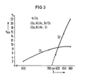
- 3 shows with curve 31 a comparison to the optical efficiency 32 of a known Si-doped diode.
- the wavelength of the emitted radiation is plotted on the abscissa and the efficiency is plotted on the ordinate. What is striking is the high electro-optical efficiency down to the visible red area.
- a gallium aluminum arsenide luminescence diode with tellurium and zinc doping has a modulability with a decay time of the luminescence which is at most 50 ns and preferably 10 to 20 ns.
- Such a diode according to the invention can even be used for video-band signal transmission in connection with devices which are intended for television games.
Landscapes
- Led Devices (AREA)
- Luminescent Compositions (AREA)
Priority Applications (1)
| Application Number | Priority Date | Filing Date | Title |
|---|---|---|---|
| AT82105471T ATE35070T1 (de) | 1981-06-24 | 1982-06-22 | Lumineszenzdiode mit hohem wirkungsgrad und hoher grenzfrequenz der modulierbarkeit. |
Applications Claiming Priority (2)
| Application Number | Priority Date | Filing Date | Title |
|---|---|---|---|
| DE3124817 | 1981-06-24 | ||
| DE19813124817 DE3124817A1 (de) | 1981-06-24 | 1981-06-24 | Lumineszenzdiode mit hohem wirkungsgrad und hoher grenzfrequenz der modulierbarkeit |
Publications (3)
| Publication Number | Publication Date |
|---|---|
| EP0068416A2 true EP0068416A2 (fr) | 1983-01-05 |
| EP0068416A3 EP0068416A3 (en) | 1985-06-26 |
| EP0068416B1 EP0068416B1 (fr) | 1988-06-08 |
Family
ID=6135281
Family Applications (1)
| Application Number | Title | Priority Date | Filing Date |
|---|---|---|---|
| EP82105471A Expired EP0068416B1 (fr) | 1981-06-24 | 1982-06-22 | Diode électroluminescente à rendement et fréquence limite de modulation élevés |
Country Status (6)
| Country | Link |
|---|---|
| US (1) | US4540451A (fr) |
| EP (1) | EP0068416B1 (fr) |
| JP (1) | JPS582081A (fr) |
| AT (1) | ATE35070T1 (fr) |
| CA (1) | CA1200882A (fr) |
| DE (1) | DE3124817A1 (fr) |
Cited By (1)
| Publication number | Priority date | Publication date | Assignee | Title |
|---|---|---|---|---|
| EP0356037A3 (fr) * | 1988-08-26 | 1991-01-09 | Hewlett-Packard Company | Méthode de fabrication d'un dispositif électro-optique avec un substrat transparent inversé |
Families Citing this family (10)
| Publication number | Priority date | Publication date | Assignee | Title |
|---|---|---|---|---|
| DE3339272A1 (de) * | 1983-10-28 | 1985-05-09 | Siemens AG, 1000 Berlin und 8000 München | Verfahren zur herstellung von a(pfeil abwaerts)3(pfeil abwaerts)b(pfeil abwaerts)5(pfeil abwaerts)-lumineszenzdioden |
| JPS60251631A (ja) * | 1984-05-28 | 1985-12-12 | Semiconductor Res Found | 不均一不純物密度分布を有する半導体装置の製造方法 |
| GB2212658B (en) * | 1987-11-13 | 1992-02-12 | Plessey Co Plc | Solid state light source |
| US5185288A (en) * | 1988-08-26 | 1993-02-09 | Hewlett-Packard Company | Epitaxial growth method |
| JPH0712094B2 (ja) * | 1988-10-19 | 1995-02-08 | 信越半導体株式会社 | 発光半導体素子用エピタキシャルウェーハの製造方法 |
| US5034334A (en) * | 1989-10-13 | 1991-07-23 | At&T Bell Laboratories | Method of producing a semiconductor laser adapted for use in an analog optical communications system |
| DE4205324A1 (de) * | 1992-02-21 | 1993-08-26 | Daimler Benz Ag | Optoelektronisches halbleiterbauelement |
| US6818153B2 (en) | 1998-10-13 | 2004-11-16 | Peter Burnell-Jones | Photocurable thermosetting luminescent resins |
| US6207077B1 (en) | 2000-02-18 | 2001-03-27 | Orion 21 A.D. Pty Ltd | Luminescent gel coats and moldable resins |
| US6905634B2 (en) | 1998-10-13 | 2005-06-14 | Peter Burnell-Jones | Heat curable thermosetting luminescent resins |
Family Cites Families (6)
| Publication number | Priority date | Publication date | Assignee | Title |
|---|---|---|---|---|
| US3537029A (en) * | 1968-06-10 | 1970-10-27 | Rca Corp | Semiconductor laser producing light at two wavelengths simultaneously |
| US3689330A (en) * | 1969-04-18 | 1972-09-05 | Sony Corp | Method of making a luminescent diode |
| JPS512393A (fr) * | 1974-06-24 | 1976-01-09 | Hitachi Ltd | |
| DE2527074B2 (de) * | 1975-06-09 | 1978-10-12 | Jury Stepanovitsch Akimov | Herstellungsverfahren für eine Anordnung mehrerer Lumineszenzdioden |
| US4199385A (en) * | 1977-09-21 | 1980-04-22 | International Business Machines Corporation | Method of making an optically isolated monolithic light emitting diode array utilizing epitaxial deposition of graded layers and selective diffusion |
| JPS5596629A (en) * | 1979-01-17 | 1980-07-23 | Matsushita Electric Ind Co Ltd | Method of epitaxially growing in liquid phase |
-
1981
- 1981-06-24 DE DE19813124817 patent/DE3124817A1/de not_active Ceased
-
1982
- 1982-06-21 JP JP57106625A patent/JPS582081A/ja active Pending
- 1982-06-22 AT AT82105471T patent/ATE35070T1/de not_active IP Right Cessation
- 1982-06-22 US US06/390,994 patent/US4540451A/en not_active Expired - Fee Related
- 1982-06-22 EP EP82105471A patent/EP0068416B1/fr not_active Expired
- 1982-06-23 CA CA000405785A patent/CA1200882A/fr not_active Expired
Cited By (1)
| Publication number | Priority date | Publication date | Assignee | Title |
|---|---|---|---|---|
| EP0356037A3 (fr) * | 1988-08-26 | 1991-01-09 | Hewlett-Packard Company | Méthode de fabrication d'un dispositif électro-optique avec un substrat transparent inversé |
Also Published As
| Publication number | Publication date |
|---|---|
| JPS582081A (ja) | 1983-01-07 |
| ATE35070T1 (de) | 1988-06-15 |
| EP0068416A3 (en) | 1985-06-26 |
| DE3124817A1 (de) | 1983-01-20 |
| US4540451A (en) | 1985-09-10 |
| CA1200882A (fr) | 1986-02-18 |
| EP0068416B1 (fr) | 1988-06-08 |
Similar Documents
| Publication | Publication Date | Title |
|---|---|---|
| EP2260516B1 (fr) | Puce semiconductrice optoélectronique et procédé de fabrication associé | |
| DE68918361T2 (de) | Elektrolumineszierende Anordnung von Verbindungshalbleitern. | |
| DE19754042A1 (de) | Epitaxialwafer für lichtemittierende Diode aus AlGaInP und lichtemittierende Diode | |
| DE4116563A1 (de) | Siliciumcarbid-leuchtdiode und verfahren zu ihrer herstellung | |
| DE112015005885B4 (de) | Optoelektronisches Bauelement | |
| EP0068416B1 (fr) | Diode électroluminescente à rendement et fréquence limite de modulation élevés | |
| EP1643554A2 (fr) | Assemblage de diodes électroluminescentes | |
| DE19615179B4 (de) | Verfahren zur Herstellung lichtemittierender Halbleiterbauelemente mit verbesserter Stabilität | |
| DE2915888C2 (fr) | ||
| DE4422220A1 (de) | Optischer Halbleitermodulator | |
| EP0752165A1 (fr) | Structure en couches quantiques | |
| DE2927454C3 (de) | Epitaxiale Scheibe zur Herstellung von Licht emittierenden Dioden | |
| DE3104082A1 (de) | "lichtemittierende hetero-junction-diode" | |
| DE2702935A1 (de) | Licht emittierendes halbleiterelement | |
| EP0584599A1 (fr) | Diode photoémettrice | |
| DE3887790T2 (de) | Lichtemittierende Halbleitervorrichtung. | |
| EP0058231B1 (fr) | Réalisation de diodes électroluminescentes ou de diodes laser ayant une surface d'emission limitée | |
| DE3324220C2 (de) | Gallium-Phosphid-Leuchtdiode | |
| DE19532204C2 (de) | Halbleitermaterial mit einem Heteroübergang | |
| DE3880442T2 (de) | Epitaxiale scheibe. | |
| DE2942508A1 (de) | Lichtemittierende diode und verfahren zu ihrer herstellung | |
| DE102004052245A1 (de) | Strahlungsemittierender Halbleiterchip und strahlungsemittierendes Halbleiterbauelement mit einem derartigen Halbleiterchip | |
| EP1153442B1 (fr) | Composant a semi-conducteur utilise pour la production d'un rayonnement electromagnetique a couleurs melangees | |
| DE2449905A1 (de) | Rotlicht emittierende galliumphosphid-diode | |
| DE10253160A1 (de) | Elektromagnetische Strahlung emittierendes Halbleiterbauelement und Verfahren zu dessen Herstellung |
Legal Events
| Date | Code | Title | Description |
|---|---|---|---|
| PUAI | Public reference made under article 153(3) epc to a published international application that has entered the european phase |
Free format text: ORIGINAL CODE: 0009012 |
|
| AK | Designated contracting states |
Designated state(s): AT BE CH FR GB IT LI NL SE |
|
| PUAL | Search report despatched |
Free format text: ORIGINAL CODE: 0009013 |
|
| AK | Designated contracting states |
Designated state(s): AT BE CH FR GB IT LI NL SE |
|
| 17P | Request for examination filed |
Effective date: 19850725 |
|
| 17Q | First examination report despatched |
Effective date: 19870114 |
|
| GRAA | (expected) grant |
Free format text: ORIGINAL CODE: 0009210 |
|
| AK | Designated contracting states |
Kind code of ref document: B1 Designated state(s): AT BE CH FR GB IT LI NL SE |
|
| PG25 | Lapsed in a contracting state [announced via postgrant information from national office to epo] |
Ref country code: NL Effective date: 19880608 |
|
| REF | Corresponds to: |
Ref document number: 35070 Country of ref document: AT Date of ref document: 19880615 Kind code of ref document: T |
|
| PG25 | Lapsed in a contracting state [announced via postgrant information from national office to epo] |
Ref country code: SE Effective date: 19880630 |
|
| GBT | Gb: translation of ep patent filed (gb section 77(6)(a)/1977) | ||
| ET | Fr: translation filed | ||
| ITF | It: translation for a ep patent filed | ||
| NLV1 | Nl: lapsed or annulled due to failure to fulfill the requirements of art. 29p and 29m of the patents act | ||
| PLBE | No opposition filed within time limit |
Free format text: ORIGINAL CODE: 0009261 |
|
| STAA | Information on the status of an ep patent application or granted ep patent |
Free format text: STATUS: NO OPPOSITION FILED WITHIN TIME LIMIT |
|
| 26N | No opposition filed | ||
| PGFP | Annual fee paid to national office [announced via postgrant information from national office to epo] |
Ref country code: AT Payment date: 19890529 Year of fee payment: 8 |
|
| PGFP | Annual fee paid to national office [announced via postgrant information from national office to epo] |
Ref country code: GB Payment date: 19890531 Year of fee payment: 8 |
|
| PGFP | Annual fee paid to national office [announced via postgrant information from national office to epo] |
Ref country code: FR Payment date: 19890622 Year of fee payment: 8 |
|
| PGFP | Annual fee paid to national office [announced via postgrant information from national office to epo] |
Ref country code: BE Payment date: 19890627 Year of fee payment: 8 |
|
| ITTA | It: last paid annual fee | ||
| PG25 | Lapsed in a contracting state [announced via postgrant information from national office to epo] |
Ref country code: LI Effective date: 19890630 Ref country code: CH Effective date: 19890630 |
|
| REG | Reference to a national code |
Ref country code: CH Ref legal event code: PL |
|
| PG25 | Lapsed in a contracting state [announced via postgrant information from national office to epo] |
Ref country code: GB Effective date: 19900622 Ref country code: AT Effective date: 19900622 |
|
| PG25 | Lapsed in a contracting state [announced via postgrant information from national office to epo] |
Ref country code: BE Effective date: 19900630 |
|
| BERE | Be: lapsed |
Owner name: SIEMENS A.G. BERLIN UND MUNCHEN Effective date: 19900630 |
|
| GBPC | Gb: european patent ceased through non-payment of renewal fee | ||
| PG25 | Lapsed in a contracting state [announced via postgrant information from national office to epo] |
Ref country code: FR Effective date: 19910228 |
|
| REG | Reference to a national code |
Ref country code: FR Ref legal event code: ST |