EP0068832A2 - Circuits logiques du type transistor-transistor - Google Patents
Circuits logiques du type transistor-transistor Download PDFInfo
- Publication number
- EP0068832A2 EP0068832A2 EP82303309A EP82303309A EP0068832A2 EP 0068832 A2 EP0068832 A2 EP 0068832A2 EP 82303309 A EP82303309 A EP 82303309A EP 82303309 A EP82303309 A EP 82303309A EP 0068832 A2 EP0068832 A2 EP 0068832A2
- Authority
- EP
- European Patent Office
- Prior art keywords
- transistor
- circuit
- collector
- whose
- type
- Prior art date
- Legal status (The legal status is an assumption and is not a legal conclusion. Google has not performed a legal analysis and makes no representation as to the accuracy of the status listed.)
- Granted
Links
Images


Classifications
-
- H—ELECTRICITY
- H03—ELECTRONIC CIRCUITRY
- H03K—PULSE TECHNIQUE
- H03K19/00—Logic circuits, i.e. having at least two inputs acting on one output; Inverting circuits
- H03K19/02—Logic circuits, i.e. having at least two inputs acting on one output; Inverting circuits using specified components
- H03K19/08—Logic circuits, i.e. having at least two inputs acting on one output; Inverting circuits using specified components using semiconductor devices
- H03K19/082—Logic circuits, i.e. having at least two inputs acting on one output; Inverting circuits using specified components using semiconductor devices using bipolar transistors
- H03K19/088—Transistor-transistor logic
Definitions
- the present invention relates to transistor-transistor logic (TTL) circuits.
- TTL transistor-transistor logic
- a fundamental TTL logic circuit can be used,in a large scale integrated circuit.
- an inverter circuit which comprises a combination of an input npn transistor and an output npn transistor and which is used as a fundamental TTL gate circuit in a large scale integrated circuit (hereinafter referred to as an LSI).
- the signal amplitude i.e., the potential difference between a high level logic signal and a low level logic signal of this inverter circuit, is very large as will be explained later, so that the propagation delay thereof is large.
- the clamp circuit is added to each of such fundamental logic circuit, the degree of integration of the LSI including such fundamental logic circuits is greatly reduced. Moreover, in such fundamental logic circuits, the potential level of the high level output signal becomes too low due to the insertion of the clamp circuit, and the noise immunity of the logic circuit deteriorates.
- a TTL fundamental logic circuit having an npn-type input transistor whose emitter is connected to an input terminal and an npn-type output transistor whose base is connected to the collector of the npn-type input transistor, whose collector is connected to a power supply voltage through a load circuit and whose emitter is connected to the ground side, the collector of the npn-type output transistor being connected to an output terminal, characterised in that the TTL fundamental logic circuit further comprises a pnp-type output transistor whose emitter is connected to the collector of the npn-type output transistor, whose base is connected to the base of the npn-type output transistor and whose collector is connected to the ground side.
- An embodiment of the present invention can decrease the signal amplitude of a fundamental logic circuit in order to reduce the propagation delay thereof.
- An embodiment of the present invention can decrease the signal amplitude of a fundamental logic circuit without greatly reducing the degree of integration of an integrated circuit including the fundamental logic circuit.
- Another embodiment of the present invention can decrease the signal amplitude of a fundamental logic circuit without unacceptably deteriorating the noise immunity thereof.
- FIG. 1 is a circuit diagram illustrating a conventional TTL fundamental logic circuit.
- the logic circuit of Fig. 1 comprises an input npn-type multi-emitter transistor Ql and an output npn-type transistor Q2 having a S chottky barrier diode, which transistor Q2 is represented in Fig. 1 by a special symbol.
- the Schottky diode is, as is known well, connected between the base and the collector electrodes in order to increase the switching speed thereof.
- Two emitter electrodes of the transistor Ql are respectively connected to the input terminals IN1 and IN2.
- the base and the collector of the transistor Q l are connected to a power supply voltage V CC through the first resistor Rl and the second resistor R2, respectively.
- the base of the transistor Q2 is connected to the collector of the transistor Ql, and the collector of the transistor Q2 is connected to the power supply voltage V CC through the third resistor R3 and to an output terminal OUT.
- the emitter of the transistor Q2 is grounded
- Fig. 2 is a waveform diagram illustrating the signals of the nodes of the circuit of Fig. 1.
- the curve Kl shows the signal at the input terminal INI
- the curve K2 of the chain line shows the ideal signal at the output terminal OUT
- the curve K3 shows the actual signal at the output terminal OUT.
- the potential of the output signal at the output terminal OUT is low, i.e., it is nearly equal to 0.3 volt.
- the transistor Q2 does not turn off until the potential of the input terminal INl falls to the threshold potential, at which time the transistor Ql is turned on.
- the threshold potential at which the transistor Ql is turned on is equal to V BE (Q2) + V BC (Q l ) - V BE (Q l ).
- V BE (Q2) and V BE (Ql) are nearly equal to each.other, the threshold potential is nearly equal to V BC (Ql).
- V BE (Q2) is the base-emitter voltage of the transistor Q2
- V BC (Ql) is the base-collector voltage of the transistor Ql
- V BE (Ql) is the base-emitter voltage of the transistor Ql. Since V BC (Ql) is approximately 0.7 V, the potential of the output terminal OUT shown by the curve K3 starts to rise at the time t 1 when the potential of the input terminal IN1 shown by the curve Kl falls approximately from 5 V to 0.7 V.
- the time difference between the ideal curve K2 and the curve K3, i.e., the propagation delay t PLH becomes very large.
- the potential of the input terminal INl rises at the time t 2 and reaches the threshold potential turning off the transistor Q1 at the time t 3 , the potential of the output terminal OUT starts to fall.
- the propagation delay t PHL at the rising edge of the input signal is smaller than the aforementioned propagation delay t PLH .
- the output signal of the output terminal OUT is supplied to a TTL fundamental logic circuit of the next stage, which has the same circuit structure as that shown in Fig. 1, as an input signal thereto, the propagation delay tp LH of the next stage is large.
- the total propagation delay of an integrated circuit including the above-mentioned TTL fundamental logic circuit becomes very large.
- the potential of the high level signal of the logic circuit of Fig. 1 is approximately equal to V CC , i.e., 5 V, the signal amplitude thereof becomes too large, so that the propagation delay is very large.
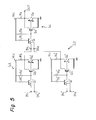
- Figure 3 is a circuit diagram illustrating another conventional TTL fundamental logic circuit whose signal amplitude is rendered to be small.
- the circuit of Fig. 3 differs from that of Fig. 1 in that it comprises a clamp circuit which is connected between the collector and the emitter of the output transistor Q2 and in which a diode D and a resistor R are connected in series.
- a current flows from the power supply voltage V cc through the resistor R3, the diode D and the resistor R to the ground. Therefore, the maximum potential of the output terminal OUT becomes approximately 0.9 through 1.0 V, and the propagation delay is greatly reduced.
- the fundamental logic circuit of Fig. 3 comprises a clamp circuit consisting of a diode and a resistor, the area occupied by each of the fundamental logic circuits in an integrated circuit device becomes large, so that the degree of integration of the integrated circuit device decreases. Moreover, since the potential of the high level signal at the output terminal OUT is approximately 0.9 through 1.0 V, the potential difference between the high level signal and the threshold potential of 0.7 V is too small and the noise immunity of the logic circuit becomes very small. Therefore, the fundamental logic circuit of Fig. 3 often operates erroneously. The objects of the present invention are to solve these problems of the conventional fundamental logic circuits. An embodiment of the present invention will be explained with reference to the attached drawings.
- Figure 4 is a circuit diagram illustrating a complementary coupled TTL fundamental logic circuit as an embodiment of the present invention.
- the logic circuit of Fig. 4 is the same as that of Fig. 1 except that the logic circuit of Fig. 4 comprises'an additional pnp transistor Q3.
- the base of the pnp transistor Q3 is connected to the base of the output npn transistor Q2 and to the collector of the input npn transistor Ql.
- the emitter of the pnp transistor Q3 is connected to the collector of the output npn transistor Q2 and the collector of the pnp transistor Q3 is grounded.
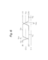
- Figure 5 illustrates a circuit in which two pre-stage fundamental logic circuits L2 and L3 are connected to the input terminal IN1 and IN2 of a fundamental logic circuit Ll, respectively.
- Each of the logic circuits Ll, L2 and L3 has the same circuit structure as that of the logic circuit of Fig. 4.
- the transistor Ql Since the input npn transistor Ql is not a transistor having.a Schottky barrier diode, the transistor Ql is completely saturated and the collector-emitter voltage thereof is approximately 0.1 V. In this condition, a current flows from the voltage source V cc through the resistor R2, the transistor Ql of the logic circuit Ll, and the transistor Q2' of the pre-stage logic circuit L2 to the ground so that the potential of the base of the pnp transistor Q3 is low and the pnp transistor Q3 is turned on. Therefore, no current is supplied to the base of the output npn transistor Q2 and the transistor Q2 is in a turned off condition.
- the potential of the output terminal OUT is in a logical high level but is much lower than the potential of the voltage source V CC .
- V OH V BE (Q 3 ) + V CE (Q l ) + V CE (Q2') is equal to 1.1 V.
- the output terminal of the pre-stage logic circuit L2 i.e., the collector of the output npn transistor Q2'
- the collector-emitter voltage V CE (Q2') rises to approximately 0.35 V
- the potential V OH of the output terminal OUT of. the logic circuit is larger than or equal to 1.1 V.
- the pnp transistor Q3 operates in a complementary manner in relation to the output npn transistor Q2, and, as illustrated in Fig. 6, the logical signal amplitude V OH - V OL at the output terminal OUT becomes a small value which is virtually equal to 0.8 V.
- the noise immunity of a fundamental logic circuit embodying the present invention can be greater than that of the conventional logic circuit of Fig. 3.
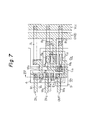
- Figure 7 is a plan view illustrating a circuit pattern of the fundamental logic circuit of Fig. 4 formed in an integrated circuit device.
- the hatched portions are metal conductor layers.
- An input terminal IN1 is connected to the first emitter electrode Ell of an input transistor Ql through a metal conducting layer M1.
- Another input terminal IN2 is connected to the second emitter electrode E12 of the transistor Ql through a metal conducting layer M2.
- the base electrode Bl of the transistor Ql is connected to a terminal of the first resistor region R1 through the metal conductor layer M3, and another terminal of the first resistor region Rl is connected to a power supply line V CC .
- the collector electrode Cl of the transistor Ql is commonly formed with the base electrode B3 of a pnp transistor Q3 and is connected to the base electrode B2 of an output transistor Q2 and to a terminal of the second resistor region R2 through a metal conducting layer M4. Another terminal of the resistor region R2 is connected to the power supply line V CC , and an output terminal OUT is connected to the emitter electrode E3 of the pnp transistor Q3 through a metal conducting layer M5.
- the emitter electrode E3 of the pnp transistor Q3 is connected to the collector electrode C2 of the output transistor Q2 and to a terminal of the third resistor region R3 through a metal conducting layer M6. Another terminal of the third resistor region R3 is connected to the power supply line V CC .
- the collector electrode C3 of the pnp transistor Q3 and the emitter electrode E2 of the output transistor Q2 are connected to a ground line GND through a metal conducting layer M7.
- Figure 8 is a cross-sectional view of the device of Fig. 7 taken along the line IIV-IIV of Fig. 7.
- 1 designates a p -type semiconductor substrate and 2 designates n -type epitaxial layers which are formed on the substrate 1 and which are separated from each other by p + -type isolation regions 3.
- a p + -type base region 4 of an input transistor Ql is formed in the n -type epitaxial layer 2 and n +- type emitter regions 5 are formed in the p +- type base region 4.
- An n +- type region 6 which operates as the collector Cl of the transistor Ql and a base B3 of a pnp transistor Q3 are formed in the n -type epitaxial region 2.
- an n -type buried layer 7 is formed between the substrate 1 and the epitaxial layer 2.
- a p +- type region 8 formed in the epitaxial layer 2 constitutes the emitter E3 of the pnp transistor Q3
- another p +- type region 9 formed in the p + -type isolation region 3 constitutes the collector C3 of the pnp transistor Q3.
- the pnp transistor Q3 is constituted of a combination of a lateral pnp structure formed by the p + -type emitter region 8, the n -type epitaxial layer 2, and the p +- type collector region 9 and a vertical pnp structure formed by the p +- type emitter region 8, the n -type epitaxial layer 2, and the p -type substrate 1.
- the p -type collector region 9 has a C-shape and is formed so as to surround the p +- type emitter region 8. Even when the thickness of the n -type epitaxial layer 2 existing between the p +- type emitter region 8 and the substrate 1 is not small enough, the pnp transistor Q3 can operate normally.
- the additional pnp transistor Q3 comprises the base region B3, the collector region C3, and the emitter region E3.
- the base region B3 is common to the collector region Cl of the input transistor Ql and the collector region C3 is common to the p-type substrate 1 and the isolation region 3 on the substrate 1.
- an inverter--type fundamental logic circuit comprises an input npn transistor and an output npn transistor, and a pnp-type transistor additionally connected parallel to the output npn transistor.
- the output npn transistor Q2 can be replaced by a usual npn transistor which does not have a Schottky barrier diode.
- the input npn transistor Ql having two emitters can be replaced by an npn transistor having any number of emitters.
Landscapes
- Engineering & Computer Science (AREA)
- Power Engineering (AREA)
- Physics & Mathematics (AREA)
- Computer Hardware Design (AREA)
- Computing Systems (AREA)
- General Engineering & Computer Science (AREA)
- Mathematical Physics (AREA)
- Logic Circuits (AREA)
Applications Claiming Priority (2)
| Application Number | Priority Date | Filing Date | Title |
|---|---|---|---|
| JP98379/81 | 1981-06-26 | ||
| JP56098379A JPS581330A (ja) | 1981-06-26 | 1981-06-26 | Ttl論理回路 |
Publications (3)
| Publication Number | Publication Date |
|---|---|
| EP0068832A2 true EP0068832A2 (fr) | 1983-01-05 |
| EP0068832A3 EP0068832A3 (en) | 1984-05-23 |
| EP0068832B1 EP0068832B1 (fr) | 1986-10-22 |
Family
ID=14218235
Family Applications (1)
| Application Number | Title | Priority Date | Filing Date |
|---|---|---|---|
| EP82303309A Expired EP0068832B1 (fr) | 1981-06-26 | 1982-06-24 | Circuits logiques du type transistor-transistor |
Country Status (4)
| Country | Link |
|---|---|
| US (1) | US4471239A (fr) |
| EP (1) | EP0068832B1 (fr) |
| JP (1) | JPS581330A (fr) |
| DE (1) | DE3273934D1 (fr) |
Cited By (1)
| Publication number | Priority date | Publication date | Assignee | Title |
|---|---|---|---|---|
| US4507575A (en) * | 1981-05-15 | 1985-03-26 | Nippon Electric Co., Ltd. | NAND Logic gate circuit having improved response time |
Families Citing this family (4)
| Publication number | Priority date | Publication date | Assignee | Title |
|---|---|---|---|---|
| US4697102A (en) * | 1984-05-28 | 1987-09-29 | Hitachi Microcomputer Engineering Co., Ltd. | Bipolar logic circuit having two multi-emitter transistors with an emitter of one connected to the collector of the other to prevent saturation |
| US4939391A (en) * | 1986-05-30 | 1990-07-03 | Advanced Micro Devices, Inc. | Programmable logic device with observability and preload circuitry for buried state registers |
| JPH03156967A (ja) * | 1989-11-15 | 1991-07-04 | Toshiba Micro Electron Kk | 出力回路 |
| JP2005117887A (ja) * | 2003-09-19 | 2005-04-28 | Auto Network Gijutsu Kenkyusho:Kk | 車載用回路ユニットの取付構造及び車載用回路ユニット |
Family Cites Families (9)
| Publication number | Priority date | Publication date | Assignee | Title |
|---|---|---|---|---|
| US3379940A (en) * | 1964-02-11 | 1968-04-23 | Nippon Electric Co | Integrated symmetrical conduction device |
| US3769530A (en) * | 1969-07-11 | 1973-10-30 | Nat Semiconductor Corp | Multiple emitter transistor apparatus |
| US3631309A (en) * | 1970-07-23 | 1971-12-28 | Semiconductor Elect Memories | Integrated circuit bipolar memory cell |
| US3742250A (en) * | 1971-04-07 | 1973-06-26 | Signetics Corp | Active region logic circuit |
| US3676713A (en) * | 1971-04-23 | 1972-07-11 | Ibm | Saturation control scheme for ttl circuit |
| US3699362A (en) * | 1971-05-27 | 1972-10-17 | Ibm | Transistor logic circuit |
| US4001868A (en) * | 1974-11-14 | 1977-01-04 | International Business Machines Corporation | Latching driver circuit and structure for a gas panel display |
| US4194132A (en) * | 1978-05-30 | 1980-03-18 | National Semiconductor Corporation | Tristate logic buffer circuit with reduced power consumption |
| JPS55113363A (en) * | 1979-02-23 | 1980-09-01 | Hitachi Ltd | Semiconductor integrated device |
-
1981
- 1981-06-26 JP JP56098379A patent/JPS581330A/ja active Pending
-
1982
- 1982-06-16 US US06/388,942 patent/US4471239A/en not_active Expired - Lifetime
- 1982-06-24 EP EP82303309A patent/EP0068832B1/fr not_active Expired
- 1982-06-24 DE DE8282303309T patent/DE3273934D1/de not_active Expired
Cited By (1)
| Publication number | Priority date | Publication date | Assignee | Title |
|---|---|---|---|---|
| US4507575A (en) * | 1981-05-15 | 1985-03-26 | Nippon Electric Co., Ltd. | NAND Logic gate circuit having improved response time |
Also Published As
| Publication number | Publication date |
|---|---|
| DE3273934D1 (en) | 1986-11-27 |
| EP0068832B1 (fr) | 1986-10-22 |
| EP0068832A3 (en) | 1984-05-23 |
| JPS581330A (ja) | 1983-01-06 |
| US4471239A (en) | 1984-09-11 |
Similar Documents
| Publication | Publication Date | Title |
|---|---|---|
| US4845386A (en) | Bi-MOS logic circuit having a totem pole type output buffer section | |
| US3868517A (en) | Low hysteresis threshold detector having controlled output slew rate | |
| US4985645A (en) | BiCMOS logic circuit having a rapid output voltage falling-down property | |
| EP0068832B1 (fr) | Circuits logiques du type transistor-transistor | |
| US3564281A (en) | High speed logic circuits and method of constructing the same | |
| US3787737A (en) | High speed/logic circuit | |
| JPH0249575B2 (fr) | ||
| US3571616A (en) | Logic circuit | |
| EP0041363B1 (fr) | Circuit trigger de Schmitt avec caractéristique d'hystérésis | |
| EP0132523A1 (fr) | Circuit logique à basse tension d'alimentation et haute vitesse de commutation | |
| US4771190A (en) | Emitter coupled logic circuit provided with pull-down resistors at respective bases of input transistors | |
| US4689502A (en) | Gate array LSI device using PNP input transistors to increase the switching speed of TTL buffers | |
| US4749885A (en) | Nonsaturating bipolar logic gate having a low number of components and low power dissipation | |
| US4239981A (en) | Fast semiconductor digital logic inverter gate | |
| US5057714A (en) | BiCMOS integrated circuit device utilizing Schottky diodes | |
| US3452216A (en) | Logic circuit | |
| EP0439894B1 (fr) | Circuit logique à semi-conducteur | |
| US4774620A (en) | Logic circuit | |
| US3437831A (en) | Logic circuit | |
| US4641047A (en) | Complex direct coupled transistor logic | |
| EP0073608B1 (fr) | Dispositif de circuit intégré du type à tranche maîtresse et son procédé de fabrication | |
| JP2551578B2 (ja) | 単一トランジスタ論理バツフア回路 | |
| EP0226722B1 (fr) | Circuit de commutation ayant un rapport vitesse/puissance élevé | |
| EP0130339B1 (fr) | Circuit logique à grande vitesse et faible consommation | |
| JPS62169464A (ja) | 半導体集積回路装置 |
Legal Events
| Date | Code | Title | Description |
|---|---|---|---|
| PUAI | Public reference made under article 153(3) epc to a published international application that has entered the european phase |
Free format text: ORIGINAL CODE: 0009012 |
|
| AK | Designated contracting states |
Designated state(s): DE FR GB |
|
| PUAL | Search report despatched |
Free format text: ORIGINAL CODE: 0009013 |
|
| RHK1 | Main classification (correction) |
Ipc: H03K 19/013 |
|
| AK | Designated contracting states |
Designated state(s): DE FR GB |
|
| 17P | Request for examination filed |
Effective date: 19840731 |
|
| GRAA | (expected) grant |
Free format text: ORIGINAL CODE: 0009210 |
|
| AK | Designated contracting states |
Kind code of ref document: B1 Designated state(s): DE FR GB |
|
| ET | Fr: translation filed | ||
| REF | Corresponds to: |
Ref document number: 3273934 Country of ref document: DE Date of ref document: 19861127 |
|
| PLBE | No opposition filed within time limit |
Free format text: ORIGINAL CODE: 0009261 |
|
| STAA | Information on the status of an ep patent application or granted ep patent |
Free format text: STATUS: NO OPPOSITION FILED WITHIN TIME LIMIT |
|
| 26N | No opposition filed | ||
| PG25 | Lapsed in a contracting state [announced via postgrant information from national office to epo] |
Ref country code: GB Effective date: 19890624 |
|
| GBPC | Gb: european patent ceased through non-payment of renewal fee | ||
| PG25 | Lapsed in a contracting state [announced via postgrant information from national office to epo] |
Ref country code: FR Free format text: LAPSE BECAUSE OF NON-PAYMENT OF DUE FEES Effective date: 19900228 |
|
| PG25 | Lapsed in a contracting state [announced via postgrant information from national office to epo] |
Ref country code: DE Effective date: 19900301 |
|
| REG | Reference to a national code |
Ref country code: FR Ref legal event code: ST |