EP0069190A2 - Kapazitiver Schalter - Google Patents
Kapazitiver Schalter Download PDFInfo
- Publication number
- EP0069190A2 EP0069190A2 EP82100735A EP82100735A EP0069190A2 EP 0069190 A2 EP0069190 A2 EP 0069190A2 EP 82100735 A EP82100735 A EP 82100735A EP 82100735 A EP82100735 A EP 82100735A EP 0069190 A2 EP0069190 A2 EP 0069190A2
- Authority
- EP
- European Patent Office
- Prior art keywords
- capacitance
- switch
- conductive
- contact
- spacing element
- Prior art date
- Legal status (The legal status is an assumption and is not a legal conclusion. Google has not performed a legal analysis and makes no representation as to the accuracy of the status listed.)
- Withdrawn
Links
- 239000012528 membrane Substances 0.000 claims abstract description 16
- 239000004020 conductor Substances 0.000 claims description 26
- 239000000758 substrate Substances 0.000 claims description 20
- 239000003990 capacitor Substances 0.000 claims description 19
- 229920000728 polyester Polymers 0.000 claims description 18
- 125000006850 spacer group Chemical group 0.000 claims description 17
- 229910052782 aluminium Inorganic materials 0.000 claims description 5
- XAGFODPZIPBFFR-UHFFFAOYSA-N aluminium Chemical compound [Al] XAGFODPZIPBFFR-UHFFFAOYSA-N 0.000 claims description 5
- 239000011159 matrix material Substances 0.000 claims description 5
- 239000000853 adhesive Substances 0.000 claims description 3
- 230000001070 adhesive effect Effects 0.000 claims description 3
- 229910052751 metal Inorganic materials 0.000 claims description 3
- 239000002184 metal Substances 0.000 claims description 3
- 239000004033 plastic Substances 0.000 claims description 3
- 239000000463 material Substances 0.000 claims 1
- 239000000428 dust Substances 0.000 abstract description 2
- 239000012530 fluid Substances 0.000 abstract 1
- 239000010410 layer Substances 0.000 description 39
- 239000004593 Epoxy Substances 0.000 description 11
- 239000012790 adhesive layer Substances 0.000 description 6
- 238000001514 detection method Methods 0.000 description 6
- 238000004519 manufacturing process Methods 0.000 description 5
- 239000004606 Fillers/Extenders Substances 0.000 description 4
- RHZWSUVWRRXEJF-UHFFFAOYSA-N indium tin Chemical compound [In].[Sn] RHZWSUVWRRXEJF-UHFFFAOYSA-N 0.000 description 4
- RYGMFSIKBFXOCR-UHFFFAOYSA-N Copper Chemical compound [Cu] RYGMFSIKBFXOCR-UHFFFAOYSA-N 0.000 description 3
- 230000005540 biological transmission Effects 0.000 description 3
- 238000010276 construction Methods 0.000 description 3
- 229910052802 copper Inorganic materials 0.000 description 3
- 239000010949 copper Substances 0.000 description 3
- 229910045601 alloy Inorganic materials 0.000 description 2
- 239000000956 alloy Substances 0.000 description 2
- 230000000881 depressing effect Effects 0.000 description 2
- 230000000694 effects Effects 0.000 description 2
- 239000004820 Pressure-sensitive adhesive Substances 0.000 description 1
- BQCADISMDOOEFD-UHFFFAOYSA-N Silver Chemical compound [Ag] BQCADISMDOOEFD-UHFFFAOYSA-N 0.000 description 1
- 229910001128 Sn alloy Inorganic materials 0.000 description 1
- NIXOWILDQLNWCW-UHFFFAOYSA-N acrylic acid group Chemical group C(C=C)(=O)O NIXOWILDQLNWCW-UHFFFAOYSA-N 0.000 description 1
- 239000003522 acrylic cement Substances 0.000 description 1
- 230000000994 depressogenic effect Effects 0.000 description 1
- 238000010586 diagram Methods 0.000 description 1
- 239000003822 epoxy resin Substances 0.000 description 1
- 238000005530 etching Methods 0.000 description 1
- 230000004927 fusion Effects 0.000 description 1
- 229910052738 indium Inorganic materials 0.000 description 1
- APFVFJFRJDLVQX-UHFFFAOYSA-N indium atom Chemical compound [In] APFVFJFRJDLVQX-UHFFFAOYSA-N 0.000 description 1
- 238000012423 maintenance Methods 0.000 description 1
- 238000000034 method Methods 0.000 description 1
- BPUBBGLMJRNUCC-UHFFFAOYSA-N oxygen(2-);tantalum(5+) Chemical compound [O-2].[O-2].[O-2].[O-2].[O-2].[Ta+5].[Ta+5] BPUBBGLMJRNUCC-UHFFFAOYSA-N 0.000 description 1
- 229920000647 polyepoxide Polymers 0.000 description 1
- 229920006267 polyester film Polymers 0.000 description 1
- 239000010970 precious metal Substances 0.000 description 1
- 238000003825 pressing Methods 0.000 description 1
- 238000001552 radio frequency sputter deposition Methods 0.000 description 1
- 230000001105 regulatory effect Effects 0.000 description 1
- 229910052709 silver Inorganic materials 0.000 description 1
- 239000004332 silver Substances 0.000 description 1
- 229910000679 solder Inorganic materials 0.000 description 1
- 238000005476 soldering Methods 0.000 description 1
- 239000013589 supplement Substances 0.000 description 1
- PBCFLUZVCVVTBY-UHFFFAOYSA-N tantalum pentoxide Inorganic materials O=[Ta](=O)O[Ta](=O)=O PBCFLUZVCVVTBY-UHFFFAOYSA-N 0.000 description 1
Images


Classifications
-
- H—ELECTRICITY
- H03—ELECTRONIC CIRCUITRY
- H03K—PULSE TECHNIQUE
- H03K17/00—Electronic switching or gating, i.e. not by contact-making and –breaking
- H03K17/94—Electronic switching or gating, i.e. not by contact-making and –breaking characterised by the way in which the control signals are generated
- H03K17/965—Switches controlled by moving an element forming part of the switch
- H03K17/975—Switches controlled by moving an element forming part of the switch using a capacitive movable element
-
- H—ELECTRICITY
- H01—ELECTRIC ELEMENTS
- H01H—ELECTRIC SWITCHES; RELAYS; SELECTORS; EMERGENCY PROTECTIVE DEVICES
- H01H13/00—Switches having rectilinearly-movable operating part or parts adapted for pushing or pulling in one direction only, e.g. push-button switch
- H01H13/70—Switches having rectilinearly-movable operating part or parts adapted for pushing or pulling in one direction only, e.g. push-button switch having a plurality of operating members associated with different sets of contacts, e.g. keyboard
- H01H13/702—Switches having rectilinearly-movable operating part or parts adapted for pushing or pulling in one direction only, e.g. push-button switch having a plurality of operating members associated with different sets of contacts, e.g. keyboard with contacts carried by or formed from layers in a multilayer structure, e.g. membrane switches
-
- H—ELECTRICITY
- H01—ELECTRIC ELEMENTS
- H01H—ELECTRIC SWITCHES; RELAYS; SELECTORS; EMERGENCY PROTECTIVE DEVICES
- H01H2239/00—Miscellaneous
- H01H2239/006—Containing a capacitive switch or usable as such
-
- H—ELECTRICITY
- H01—ELECTRIC ELEMENTS
- H01H—ELECTRIC SWITCHES; RELAYS; SELECTORS; EMERGENCY PROTECTIVE DEVICES
- H01H2239/00—Miscellaneous
- H01H2239/01—Miscellaneous combined with other elements on the same substrate
Definitions
- This invention relates to capacitance-type switches.
- an improved capacitance-type switch can be provided if an electrically integral capacitance spacing layer is provided over a plurality of switch zones.
- membrane capacitance-type switches may be usably and desirably provided.
- I provide at one end of the capacitance spacer a folded-over portion; I use a screened insulating epoxy resin as a mechanical spacer; and I use a layer comprising indium to facilitate electrical connecting.
- the capacitance spacing element can be located other than directly adjacent the contacts, and switching elements remotely spaced from one another can share a common capacitance spacing element.
- Devices according to my invention have many advantages. Because the area of the capacitance spacer layer is increased, the difference between unactuated and actuated capacitance is greater, for a greater signal-to-noise ratio. Furthermore, in its membrane switch aspect there is provided a sealed capacitance-type switch, protected against dust and vapors. Long life is provided. Because current flows can be made extremely small, not only can much smaller quantities of metal be used for conductors and contacts, but less expensive, non-precious metals may be used for the most part. Other advantages will appear in the following discussion.
- a membrane switch i.e., a switch in which a flexible layer is flexed in order to produce a signal output
- the signal output is produced by a large change in capacitance
- the device may perhaps be most understandably explained by an initial description of how it is made.
- top layer 10 It comprises 5-mil thick transparent polyester layer 10, on the bottom surface of'which has been vacuum deposited thereon through a suitable mask of multiplicity of round pads 12 and conductors 14, of copper, 1500 ⁇ ngstrom units thick.
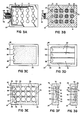
- Fig. 3B is a bottom view of said top layer 10 showing positioned over the surfaces, including the pads and connectors, illustrated in Fig. 3A, a layer 16 of insulating epoxy (one mil thick), ultraviolet curable and capable (like the other elements.of the switch) of withstanding elevated temperature and humidity (e.g., 85°C and 85% R.H.), screened through a mask prior to curing, and including a multiplicity of zones 18 in which, corresponding with the locations of pads 12, the epoxy is laid down, not in an uninterrupted layer as throughout most of the device, but in sets of grid lines 20.
- the layer of epoxy is also relieved at three areas 21, corresponding with the location of contact areas 22 (shown in Fig. 3A).
- Fig. 3C is a plan view of bottom layer 24, also of five mil thickness transparent polyester film, on which has been deposited, through a mask, a 1/2-mil thick layer 26 of pressure-sensitive acrylic adhesive, interrupted by generally circular zones 28 corresponding to the locations of conducting pad zones 22 on the top layer 10.
- Fig. 3D is a plan view of the bottom layer 24 following the next step in the manufacturing process, namely, the assembly of the three elongated strips 30, which are. held in place by adhesive layer 26, and are formed from 1/4-mil polyester on each outer surface of which is vacuum deposited by R F sputtering layers 1000 Angstrom units in thickness of aluminum.
- Fig. 3E is a plan view of bottom layer 24 after the next step in manufacture of the device.
- this step there is deposited through a mask, . over the area indicated in dots, a layer 31 of acrylic pressure-sensitive adhesive one mil in thickness. As shown in the drawings, this step leaves uncoated areas 32 corresponding to the contact areas 22 in top element 10 and areas 34 corresponding to the pads 12 of element 10.
- the step just described leaves extending freely the tips 36 of strips 30. These tips are then folded up around edges 38 of adhesive layer 31, as illustrated in Fig. 3F, as well as in Fig. 2.
- Dots 40 of a silver filled conductive epoxy (Amicon 3050, sold by Amicon Corporation of Lex- ington, Massachusetts) are then deposited along the fold line of the strips 30, to supplement conductivity through the outer aluminum layers of strips 30 and make contact with pads 22.
- top and bottom elements to be assembled into the switch separately, and while each is part of a web of greater width than the final width dimension of the switch.
- portions to define the tail 42 are cut out before the upper and lower portions are assembled.
- a cut is made to define edge 46 of the lower portion as well as a window of which the edge 46 is one of the four sides to permit movement therethrough for soldering of tail 42.
- They are then assembled, and held together by adhesive layer 31. Next they pass over a roller which causes tail 42 to extend in a direction facilitating adding thereto, over the conductor areas 44, by standard solder wave techniques, one mil thick layer of 50% indium-50% tin alloy.
- a suitable detection circuit is disclosed in Fig. 4.
- a single switch shown as indicated at 50 corresponds to one of the 12 switching areas shown in the preferred embodiment.
- Clock 52 sends. out square wave pulses at a frequency of 2kHz through inverter 54 and resistance 56 into one side of switch 50 and simply through resistance 58 into the other. So long as the switch 50 is not actuated, so that both air capacitor 60 and polyester capacitor 62 are in the circuit, current flows through inverter 64 and transmission gate 66 are insufficient to transmit signals past RC networks 68 and 70.
- signals do pass RC networks 68 and 70, providing output signals at transmission gates 72 and 74, the former providing information, in the preferred embodiment, of the X position of the switch pressed, and transmission gate 74 providing similar information as to the Y position.
- a pad 12 is pushed downwardly by flexing flexible layer 10, which carries it, until pad 12 engages a strip 30.
- the amount of force required to do this may be regulated partially by the spacing of epoxy grid lines 20; the more closely spaced are the grid bars 20, the more difficult is it to push down layer 10 and pad 12 between them to engage strip 30.
- This in effect eliminates one of two capacitors in series (the air capacitor 60), leaving the polyester capacitor, causing the capacitance of the circuit through this contact made to increase enormously.
- the. capacitance increases from 30 picofarads to 10 nanofarads--i.e., over three hundred times.
- polyester layer producing the large capacitance could be substituted, for example, a deposited layer of tantalum pentoxide, which has a dielectric constant many times that of polyester.
- a diecut polyester spacer could be used.
- Conductor areas could be made by printing or etching.
- the polyester capacitor strip could be folded on itself to produce increased capacitance.
- the device could be a common ground one, with a separate lead coming off each conductive pad; here the other lead to all the pads might desirably be a single large capacitor spacer (as opposed to the three strips shown in the embodiment described).
- the entire device could be made transparent, so that it might be mounted on the face of a CRT.
- the substrate of the device could be made rigid.
- the capacitor spacing layer is a single sheet substantially the size of the overall device and located in it below a layer carrying on it a plurality of X-row pads and beneath it a layer of Y-column pads, with spacers between the central layer and each of the other two.
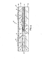
- FIG. 6 there is shown a portion of capacitance switch 10 having switching elements arranged in positions corresponding to positions of keys of a computer terminal.
- Switch 10 has a plurality of switching elements with their movable contacts located directly over elongated capacitance spacing elements (e.g., switching element 12 with movable contact 14 over elongated capacitance spacing element 16) and a plurality of switching elements horizontally spaced from their associated elongated capacitance spacing elements (e.g., switching element 18 with movable upper contact 20 over lower contact 22 connected by conductor 23 to elongated capacitance spacing element 24--Fig. 9).
- elongated capacitance spacing elements e.g., switching element 12 with movable contact 14 over elongated capacitance spacing element 16
- switching elements horizontally spaced from their associated elongated capacitance spacing elements e.g., switching element 18 with movable upper contact 20 over lower contact 22 connected by conductor 23 to elongated capacitance spacing element 24--Fig. 9).
- Movable contacts 14, 20 are copper pads vacuum-deposited on the lower surface of flexible polyester sheet 26. Adhered above layer 26 by adhesive layer 28 is plastic overlay 30 having indicia inked thereon, index 32 being the-letter "z", index 34 being the symbol "SH”. (See Fig. 7.) On the bottom surface of flexible sheet 26 and contacts 14, 20 is cured epoxy layer 36, which is interrupted in the switching element regions to leave the majority of the lower surfaces of contacts 14, 20 exposed. Elongated capacitance spacing element 16 is adhered therebelow by adhesive layer 38 and consists of 1/4 mil thick polyester with RF sputtered layers of aluminum on the upper and lower surfaces. The bottom surface of capacitance spacing element 16 is attached by adhesive layer 40 to bottom polyester sheet 42. Contact 22 is carried by bottom sheet 42.
- Each switching element includes an air capacitor (e.g., contact 20 separated from contact 22 by air; contact 14 separated from upper conductive surface of capacitance spacing element 16 by air) of low capacitance connected in series with a polyester capacitor (e.g., large-area capacitance spacing element 16) of high capacitance.
- the capacitances of the switching elements are thus low when the contacts are in the ordinarily open positions shown in Fig. 6, and high when the air capacitors are short-circuited by bringing the upper movable contacts in electrical engagement with the upper surfaces of their associated capacitance switching elements.
- Connections to external circuitry are provided by conductors carried by the lower surface of polyester sheet 26 (Figs. 6' and 8).
- Contact 14 is connected to column conductor 44.
- the lower aluminum surface of capacitance spacing element 16 is connected at its folded-over end 45 by conductive epoxy 46 and conductive pad 48 to row conductor 50.
- Contact 20 is connected to column conductor 52.
- Row conductor 50, column conductors 44, 52 and other similar conductors are all connected to tail 54 for connection to external circuitry.
- Fig. 7 shows overlay 30 with its indicia associated with the plurality of switching elements
- Fig. 8 shows transparent flexible sheet 26 with conductive members on its bottom, the contacts being in the same orientation as their associated indicia shown in Fig. 7.
- the conductive members include a plurality of movable contacts (e.g., larger circles similar to contacts 14, 20), row conductive pads (e.g., smaller circles similar to conductive pad 48), and conductive lines (e.g., conductive lines 44, 50, 52) ending at tail 54.
- Fig. 9 shows bottom layer 42 with nine elongated capacitance spacing elements designated R 1 through R 9 to indicate rows of switching elements, lower switch contacts (e.g., contact 22), lower contact pads 56 (similar to conductive pad 48), and conductive lines (e.g., line 23).
- a vertical solid line on a capacitance spacing element indicates that the element is folded over upward, as element 16 (also designated R 4 ) is, to make electrical contact of the lower conductive surface with a pad on the bottom of upper sheet 26.
- a vertical dashed line on a capacitance spacing element indicates that the element is folded over downward to make contact of its upper conductive surface with a pad 56 on bottom sheet 42; e.g., the upper surface of end 58 of row 9 is electrically connected to pad 56 with conductive epoxy similar to epoxy 46.
- the folded over construction of capacitance spacing elements permits carrying all of the conductors for connection to external circuitry by flexible polyester sheet 26.
- the folded over construction also provides a simple connection between the upper surfaces of the capacitance spacing elements and the remotely located contacts.
- switching element 12 corresponds to row 4 (tail conductor 103) and column 1 (tail conductor 109).
- the three switching elements in row 9 have columns exclusively used by a single switching element.
- switching element 18 corresponds to row 9 (tail conductor 101), and the "Shift" column (tail conductor 102).
- a switching element is activated by depressing overlay 30 at a location associated with an index. For example if overlay 30 is depressed at index 32, contact 14 engages the upper surface of capacitance spacing element 16, and this in effect eliminates one of the two capacitors in series (air capacitor between contact 14 and the upper conductive surface of element 16), leaving the polyester capacitor (capacitance spacing element 16), and causing the capacitance of the circuit through switching element 12 to increase enormously.
- the increase of capacitance appears between tail conductor 103 and tail conductor 109 and is detected by the detection circuitry (not shown) as row 4, column 1.
Landscapes
- Push-Button Switches (AREA)
- Investigating Or Analyzing Materials By The Use Of Electric Means (AREA)
- Switches That Are Operated By Magnetic Or Electric Fields (AREA)
- Separation Using Semi-Permeable Membranes (AREA)
Applications Claiming Priority (2)
| Application Number | Priority Date | Filing Date | Title |
|---|---|---|---|
| US278658 | 1981-06-29 | ||
| US06/278,658 US4400758A (en) | 1981-06-29 | 1981-06-29 | Capacitance switch arrangement |
Publications (2)
| Publication Number | Publication Date |
|---|---|
| EP0069190A2 true EP0069190A2 (de) | 1983-01-12 |
| EP0069190A3 EP0069190A3 (de) | 1983-04-06 |
Family
ID=23065833
Family Applications (1)
| Application Number | Title | Priority Date | Filing Date |
|---|---|---|---|
| EP82100735A Withdrawn EP0069190A3 (de) | 1981-06-29 | 1982-02-02 | Kapazitiver Schalter |
Country Status (2)
| Country | Link |
|---|---|
| US (1) | US4400758A (de) |
| EP (1) | EP0069190A3 (de) |
Cited By (4)
| Publication number | Priority date | Publication date | Assignee | Title |
|---|---|---|---|---|
| DE3640866A1 (de) * | 1986-01-07 | 1987-07-09 | Alps Electric Co Ltd | Membranschalter |
| EP0244698A1 (de) * | 1986-05-05 | 1987-11-11 | Siemens Aktiengesellschaft | Detektormatte und Verfahren zu ihrer Herstellung |
| EP0268497A3 (en) * | 1986-11-20 | 1989-02-08 | Brother Kogyo Kabushiki Kaisha | Printed circuit board |
| EP0365787A3 (de) * | 1988-10-25 | 1991-11-27 | W.H. Brady Co. | Kapazitive Membrantastatur mit kapazitiver Ankopplung zwischen Leiterbahnen und/oder kapazitiver Ankopplung in Leiterbahnen |
Families Citing this family (17)
| Publication number | Priority date | Publication date | Assignee | Title |
|---|---|---|---|---|
| US4650314A (en) * | 1983-10-07 | 1987-03-17 | Grunwald Robert F | Film inspection machine |
| US4562315A (en) * | 1984-09-20 | 1985-12-31 | W. H. Brady Co. | Capacitance membrane switch |
| US5087825A (en) * | 1990-02-15 | 1992-02-11 | Nartron Corporation | Capacity responsive keyboard |
| US5153572A (en) * | 1990-06-08 | 1992-10-06 | Donnelly Corporation | Touch-sensitive control circuit |
| US5157273A (en) * | 1990-06-08 | 1992-10-20 | Donnelly Corporation | Modular power outlet strip |
| US5189417A (en) * | 1990-10-16 | 1993-02-23 | Donnelly Corporation | Detection circuit for matrix touch pad |
| US5225959A (en) * | 1991-10-15 | 1993-07-06 | Xerox Corporation | Capacitive tactile sensor array and method for sensing pressure with the array |
| US5572205A (en) * | 1993-03-29 | 1996-11-05 | Donnelly Technology, Inc. | Touch control system |
| US5594222A (en) * | 1994-10-25 | 1997-01-14 | Integrated Controls | Touch sensor and control circuit therefor |
| ATE295629T1 (de) | 1996-12-10 | 2005-05-15 | David W Caldwell | Differentieller berührungssensor und steuerungsschaltung dafür |
| US6059575A (en) * | 1998-10-21 | 2000-05-09 | Murphy; Kevin C. | Tactile recognition input device and overlay for use with an input device |
| US7906875B2 (en) | 1999-01-19 | 2011-03-15 | Touchsensor Technologies, Llc | Touch switches and practical applications therefor |
| US6320282B1 (en) | 1999-01-19 | 2001-11-20 | Touchsensor Technologies, Llc | Touch switch with integral control circuit |
| US7989725B2 (en) * | 2006-10-30 | 2011-08-02 | Ink-Logix, Llc | Proximity sensor for a vehicle |
| TWM353598U (en) * | 2008-11-05 | 2009-03-21 | Darfon Electronics Corp | Membrane circuit board |
| EP2459882A1 (de) * | 2009-07-27 | 2012-06-06 | TouchSensor Technologies, L.L.C. | Steuerung und verfahren für füllstandmessung |
| US20110128154A1 (en) * | 2009-12-01 | 2011-06-02 | Flow-Rite Controls, Ltd. | Battery electrolyte level indicator |
Family Cites Families (6)
| Publication number | Priority date | Publication date | Assignee | Title |
|---|---|---|---|---|
| US3696908A (en) * | 1970-11-09 | 1972-10-10 | Sperry Rand Corp | Capacitive key |
| US3797630A (en) * | 1971-07-12 | 1974-03-19 | Alphanumeric Holdings Ltd | Keyboard for electronic circuit |
| GB1443174A (en) * | 1973-04-06 | 1976-07-21 | Alphameric Keyboards Ltd | Keyboards for electronic circuits |
| US3921167A (en) * | 1974-06-14 | 1975-11-18 | Ibm | Capacitive circuitboard |
| GB1582640A (en) * | 1976-10-18 | 1981-01-14 | Alphameric Keyboards Ltd | Keyboards for electronic circuits |
| US4263659A (en) * | 1978-03-27 | 1981-04-21 | Canon Kabushiki Kaisha | Electronic instrument with a flexible keyboard |
-
1981
- 1981-06-29 US US06/278,658 patent/US4400758A/en not_active Expired - Lifetime
-
1982
- 1982-02-02 EP EP82100735A patent/EP0069190A3/de not_active Withdrawn
Cited By (4)
| Publication number | Priority date | Publication date | Assignee | Title |
|---|---|---|---|---|
| DE3640866A1 (de) * | 1986-01-07 | 1987-07-09 | Alps Electric Co Ltd | Membranschalter |
| EP0244698A1 (de) * | 1986-05-05 | 1987-11-11 | Siemens Aktiengesellschaft | Detektormatte und Verfahren zu ihrer Herstellung |
| EP0268497A3 (en) * | 1986-11-20 | 1989-02-08 | Brother Kogyo Kabushiki Kaisha | Printed circuit board |
| EP0365787A3 (de) * | 1988-10-25 | 1991-11-27 | W.H. Brady Co. | Kapazitive Membrantastatur mit kapazitiver Ankopplung zwischen Leiterbahnen und/oder kapazitiver Ankopplung in Leiterbahnen |
Also Published As
| Publication number | Publication date |
|---|---|
| US4400758A (en) | 1983-08-23 |
| EP0069190A3 (de) | 1983-04-06 |
Similar Documents
| Publication | Publication Date | Title |
|---|---|---|
| EP0069190A2 (de) | Kapazitiver Schalter | |
| CA1173131A (en) | Capacitance switch | |
| US4373122A (en) | Capacitance switch | |
| US4373124A (en) | Capacitance switch | |
| US4431882A (en) | Transparent capacitance membrane switch | |
| US5062198A (en) | Method of making a transparent touch screen switch assembly | |
| US4017697A (en) | Keyboard membrane switch having threshold force structure | |
| CA1061434A (en) | Capacitive two dimensional tablet with single conductive layer | |
| CA1065761A (en) | Membrane keyboard apparatus capable of providing sequential output signals | |
| EP0044342B1 (de) | Druckempfindlicher piezoelektrischer polymer-signalgenerator | |
| EP0435438B1 (de) | Eingabesystem mit berührungsempfindlicher Widerstandsfilmtafel | |
| CN100517203C (zh) | 触摸屏 | |
| US3593115A (en) | Capacitive voltage divider | |
| US4857684A (en) | Capacitance membrane switchcore with intertrace capacitive coupling and/or intratrace capacitive coupling | |
| US4920342A (en) | Membrane switchcores with high resisitivity ink circuits | |
| US4484038A (en) | Membrane touch panel having improved conductor construction | |
| US3691555A (en) | Electronic keyboard | |
| US4609792A (en) | Encoding keyboard | |
| US3701869A (en) | Touch switch array panel | |
| KR920007747B1 (ko) | 쉬트형 스위치소자(Sheet switch) | |
| US4412209A (en) | RC Array | |
| US4623768A (en) | Foldable membrane switch with fold remote from contact-carrying panels | |
| US4429301A (en) | Means for decoding a switch array | |
| JPS6039718A (ja) | スイツチのマトリツクス構成 | |
| EP0134853A1 (de) | Mittel zum Dekodieren eines Schaltfeldes |
Legal Events
| Date | Code | Title | Description |
|---|---|---|---|
| PUAI | Public reference made under article 153(3) epc to a published international application that has entered the european phase |
Free format text: ORIGINAL CODE: 0009012 |
|
| AK | Designated contracting states |
Designated state(s): AT BE DE FR GB IT LU NL |
|
| PUAL | Search report despatched |
Free format text: ORIGINAL CODE: 0009013 |
|
| AK | Designated contracting states |
Designated state(s): AT BE DE FR GB IT LU NL |
|
| 17P | Request for examination filed |
Effective date: 19830712 |
|
| STAA | Information on the status of an ep patent application or granted ep patent |
Free format text: STATUS: THE APPLICATION HAS BEEN WITHDRAWN |
|
| 18W | Application withdrawn |
Withdrawal date: 19850806 |
|
| RIN1 | Information on inventor provided before grant (corrected) |
Inventor name: FRAME, NORMAN JOSEPH Inventor name: WALBER, JAMES PETER |