EP0069265A1 - Structure de masque pour lithographie à rayons X et procédé pour sa fabrication - Google Patents
Structure de masque pour lithographie à rayons X et procédé pour sa fabrication Download PDFInfo
- Publication number
- EP0069265A1 EP0069265A1 EP82105379A EP82105379A EP0069265A1 EP 0069265 A1 EP0069265 A1 EP 0069265A1 EP 82105379 A EP82105379 A EP 82105379A EP 82105379 A EP82105379 A EP 82105379A EP 0069265 A1 EP0069265 A1 EP 0069265A1
- Authority
- EP
- European Patent Office
- Prior art keywords
- mask
- lattice
- mask substrate
- ray
- substrate
- Prior art date
- Legal status (The legal status is an assumption and is not a legal conclusion. Google has not performed a legal analysis and makes no representation as to the accuracy of the status listed.)
- Granted
Links
Images



Classifications
-
- G—PHYSICS
- G03—PHOTOGRAPHY; CINEMATOGRAPHY; ANALOGOUS TECHNIQUES USING WAVES OTHER THAN OPTICAL WAVES; ELECTROGRAPHY; HOLOGRAPHY
- G03F—PHOTOMECHANICAL PRODUCTION OF TEXTURED OR PATTERNED SURFACES, e.g. FOR PRINTING, FOR PROCESSING OF SEMICONDUCTOR DEVICES; MATERIALS THEREFOR; ORIGINALS THEREFOR; APPARATUS SPECIALLY ADAPTED THEREFOR
- G03F1/00—Originals for photomechanical production of textured or patterned surfaces, e.g., masks, photo-masks, reticles; Mask blanks or pellicles therefor; Containers specially adapted therefor; Preparation thereof
- G03F1/22—Masks or mask blanks for imaging by radiation of 100nm or shorter wavelength, e.g. X-ray masks, extreme ultraviolet [EUV] masks; Preparation thereof
-
- H—ELECTRICITY
- H10—SEMICONDUCTOR DEVICES; ELECTRIC SOLID-STATE DEVICES NOT OTHERWISE PROVIDED FOR
- H10P—GENERIC PROCESSES OR APPARATUS FOR THE MANUFACTURE OR TREATMENT OF DEVICES COVERED BY CLASS H10
- H10P95/00—Generic processes or apparatus for manufacture or treatments not covered by the other groups of this subclass
-
- Y—GENERAL TAGGING OF NEW TECHNOLOGICAL DEVELOPMENTS; GENERAL TAGGING OF CROSS-SECTIONAL TECHNOLOGIES SPANNING OVER SEVERAL SECTIONS OF THE IPC; TECHNICAL SUBJECTS COVERED BY FORMER USPC CROSS-REFERENCE ART COLLECTIONS [XRACs] AND DIGESTS
- Y10—TECHNICAL SUBJECTS COVERED BY FORMER USPC
- Y10S—TECHNICAL SUBJECTS COVERED BY FORMER USPC CROSS-REFERENCE ART COLLECTIONS [XRACs] AND DIGESTS
- Y10S430/00—Radiation imagery chemistry: process, composition, or product thereof
- Y10S430/167—X-ray
-
- Y—GENERAL TAGGING OF NEW TECHNOLOGICAL DEVELOPMENTS; GENERAL TAGGING OF CROSS-SECTIONAL TECHNOLOGIES SPANNING OVER SEVERAL SECTIONS OF THE IPC; TECHNICAL SUBJECTS COVERED BY FORMER USPC CROSS-REFERENCE ART COLLECTIONS [XRACs] AND DIGESTS
- Y10—TECHNICAL SUBJECTS COVERED BY FORMER USPC
- Y10S—TECHNICAL SUBJECTS COVERED BY FORMER USPC CROSS-REFERENCE ART COLLECTIONS [XRACs] AND DIGESTS
- Y10S430/00—Radiation imagery chemistry: process, composition, or product thereof
- Y10S430/167—X-ray
- Y10S430/168—X-ray exposure process
Definitions
- the present invention relates to a mask structure for X-ray lithography and a method for manufacturing the same.
- lithography techniques have been recently developed to provide fine patterning of semiconductor devices with light rays, electron beams and X-rays.
- X-ray lithography is receiving a great deal of attention as a technique which can provide fine patterning in the order of submicrons.
- the following problems remain unsolved in a mask structure used in X-ray lithography.
- Fig. 1 is a sectional view schematically showing a conventional mask structure for X-ray lithography.
- a mask pattern 2 comprising an X-ray absorbing material such as gold is formed on the surface of a substrate 1 comprising an X-ray transmitting material.
- Support members 3 are mounted on the lower surface of the substrate 1.
- the substrate 1 must be made of a material with a high X-ray transmittance and must have a thickness of not more than several um.
- the substrate 1 is generally made of an inorganic material such as silicon oxide or silicon nitride. However, such a material is brittle and has a low mechanical strength, which does not allow enlargement of the area of the substrate 1 beyond several square millimeters.
- the support members 3 must be mounted at every several millimeters, resulting in a complex structure. Further, the width of the support member 3 is as wide as several mm. Portions of the substrate 1 which are supported by the support members 3 cannot be used for X-ray exposure. An effective area of the mask structure which is used as a mask is small.
- a substrate 4 is made of an organic material such as a synthetic resin instead of an inorganic material, the support members need not be used in great number. As a result, a mask structure of a large area can be achieved.
- the substrate 4 described above is so expandable and contractible that the mask dimensions may not be stabilized. The impreciseness of the substrate dimensions is a decisive drawback in fine patterning of the semiconductor device.
- an object of the present invention to provide a mask structure for X-ray lithography, which provides a substrate having a large area without forming a number of support members, and which achieves stable fine patterning.
- a mask structure for X-ray lithography comprising:
- a method for manufacturing a mask structure for X-ray lithography comprising the steps of:
- Fig. 3A is a plan view of a mask structure for X-ray lithography according to a first embodiment of the present invention
- Fig. 3B is a plan view thereof along the line A - A in Fig. 3A.
- a lattice-shaped metal film 11 is embedded in a lattice-shaped slit formed in a mask substrate 12 of an X-ray transmitting material.
- the mask substrate 12 is divided into a plurality of substrate elements by the lattice-shaped metal film 11. Each substrate element is surrounded by the metal film 11.
- a ring-shaped support member 13 is formed on the rear periphery of a disc-shaped body made of the mask substrate 12 and the metal film 11. Slit pattern formed in the substrate elements of the mask substrate 1 which are divided by the metal film are filled with a mask pattern of an X-ray absorbing material.
- the mask substrate 12 having a large area has a high mechanical strength and stable dimensions as a whole.
- the width of the lattice-shaped metal film 11 is as small as 100 p, and the effective area which may be used for X-ray exposure is great.
- a semiconductor wafer is divided into chips by lattice-shaped dicing lines, and the mask pattern thereon is projected. Since the width of the dicing line is as small as about 100 p, the area of the mask substrate is effectively used if the lattice-shaped metal film 11 is formed corresponding to the positions of the dicing lines of the mask structure.
- the X-ray transmitting material which constitutes the mask substrate 12 may comprise an inorganic material such as silicon oxide, silicon nitride, doped or undoped polycrystalline silicon, boron nitride, or a multilayered structure thereof such as a two-layer structure of silicon oxide and silicon nitride, and a three-layer structure of silicon nitride, silicon oxide and silicon nitride.
- an organic material of a synthetic resin such as polyimide may be used. If an inorganic material is used which has stable dimensions for the mask substrate but which has a low mechanical strength, the mechanical strength is improved by the lattice-shaped metal film. However, if an organic material is used which has a high mechanical strength but which has unstable dimensions, the unstable dimensions are improved by the lattice-shaped metal film.
- the lattice-shaped metal film may comprise any metal. However,.if the lattice-shaped metal film is formed simultaneously as the mask pattern is formed, the same material as the mask pattern, that is, the X-ray absorbing material must be used.
- the X-ray absorbing material constituting the mask pattern may be a heavy metal such as gold and platinum.
- a material constituting the ring-shaped support member may be silicon or glass.
- a silicon support plate 21 having a crystal orientation of (100), a resistivity of 0.001 ⁇ -cm, and a diameter of 4" is oxidized by thermal oxidation to form a thermal oxide 0
- a silicon oxide film 23 of about 1 pm is deposited by the vapor growth method on the upper surface of the silicon support plate 21 through the thermal oxide film 22.
- a photoresist film is formed on the surface of the silicon oxide film 23 and is patterned by photolithography to form a resist pattern 24, as shown in Fig. 4C.
- the oxide films 22 and 23 which are sequentially formed on the upper surface of the support plate 21 are selectively etched by reactive ion etching using a gas mixture of CF 4 and H 2 as a reactive gas. Thereafter, the resist pattern 24 is removed (Fig. 4D).
- An oxide film 23' having a desired pattern is obtained.
- the oxide film 23' corresponds to the mask substrate shown in Figs. 3A and 3B.
- a gold film 25 of about 0.8 pm thickness is formed only in the slits of the oxide film 23'.
- the gold film 25 comprises a lattice-shaped metal film 25a and a mask pattern 25b.
- the lattice-shaped metal film 25a and the mask pattern 25b are simultaneously formed. Further, part of the thermal oxide film 22 at the central rear portion of the silicon support plate 21 is etched. Finally, the whole is dipped in an etching solution which contains KOH as the major component to leave only a peripheral portion 21' and to etch the 60-mm diameter portion of the silicon support plate 21.
- the peripheral portion 21' of the residual silicon support plate 21 corresponds to a support member 13 shown in Fig. 3B.
- the mask structure shown in Figs. 3A and.3B is obtained.
- a special manufacturing step is not required.
- the insulating material is used as the mask substrate and electroplating is utilized to form the lattice-shaped metal film. Therefore, the lattice-shaped metal film and the mask pattern are simultaneously formed.
- a conductive material such as impurity-doped polycrystalline silicon is used as the material of the mask substrate, the metal film cannot be selectively formed by electroplating only in the slits formed in the mask substrate.
- the following method is adopted. After predetermined slits are formed in the mask substrate, a metal is deposited by vacuum evaporation or the like on the entire surface including the inside portions of the slits. Thereafter, a resist film is formed on the metal film to a predetermined thickness and the surface of the resist film is made smooth. The metal film only on the mask substrate is etched by dry etching, so that the metal remains only in the slits.
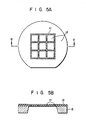
- Fig. 5A is a plan view of the mask structure for X-ray lithography according to a second embodiment of the present invention
- Fig. 5B is a sectional view thereof along the line B - B in Fig. 5A.
- the same reference numerals used in Figs. 3A and 3B denote the same parts in Figs. 5A and 5B and the mask pattern is omitted for illustrative convenience.
- the mask structure for X-ray lithography in the second embodiment is the same as that in the first embodiment.except that the lattice-shaped metal film 11 is formed only at the center of the mask structure.
- a method for manufacturing the mask structure in the second embodiment is the same as that in the first embodiment, so the same effects as in the first embodiment are obtained.
- the mask structure according to the second embodiment is employed to form the mask pattern only at the center thereof. In this case, the width of the ring-shaped support plate 21 of silicon is large enough, so the lattice-shaped metal film need not be formed at the periphery thereof.
- Fig. 6A is a plan view of a mask structure for X-ray lithography according to a third embodiment of the present invention
- Fig. 6B is a sectional view thereof along the line C - C in Fig. 6A.
- the same reference numerals used in Figs. 3A and 3B denote the same parts in Figs. 6A and 6B, and the mask pattern is omitted in the same manner as in Figs. 5A and 5B.
- the mask structure for X-ray lithography in the third embodiment is the same as that in the first embodiment except that the lattice-shaped metal film 11 is formed at the center of the mask structure and a metal film 31 is formed therearound.
- the mask substrate at the periphery of the mask structure shown in Figs. 5A and 5B is replaced with the metal film 31.
- a method for manufacturing the mask structure of the third embodiment is the same as that of the first embodiment, so that the same effects obtained in the first embodiment are obtained.
- the mask pattern is embedded in the slit formed in the mask substrate.
- the present invention is not limited to the above arrangement.
- the mask pattern may be formed on the upper surface of the mask substrate 12.
Landscapes
- Physics & Mathematics (AREA)
- General Physics & Mathematics (AREA)
- Preparing Plates And Mask In Photomechanical Process (AREA)
- Exposure Of Semiconductors, Excluding Electron Or Ion Beam Exposure (AREA)
Applications Claiming Priority (2)
| Application Number | Priority Date | Filing Date | Title |
|---|---|---|---|
| JP97705/81 | 1981-06-24 | ||
| JP9770581A JPS57211732A (en) | 1981-06-24 | 1981-06-24 | X ray exposing mask and manufacture thereof |
Publications (2)
| Publication Number | Publication Date |
|---|---|
| EP0069265A1 true EP0069265A1 (fr) | 1983-01-12 |
| EP0069265B1 EP0069265B1 (fr) | 1986-04-09 |
Family
ID=14199329
Family Applications (1)
| Application Number | Title | Priority Date | Filing Date |
|---|---|---|---|
| EP82105379A Expired EP0069265B1 (fr) | 1981-06-24 | 1982-06-18 | Structure de masque pour lithographie à rayons X et procédé pour sa fabrication |
Country Status (4)
| Country | Link |
|---|---|
| US (1) | US4451544A (fr) |
| EP (1) | EP0069265B1 (fr) |
| JP (1) | JPS57211732A (fr) |
| DE (1) | DE3270382D1 (fr) |
Cited By (6)
| Publication number | Priority date | Publication date | Assignee | Title |
|---|---|---|---|---|
| DE3338717A1 (de) * | 1983-10-25 | 1985-05-02 | Siemens AG, 1000 Berlin und 8000 München | Verfahren zur herstellung einer roentgenmaske mit metalltraegerfolie |
| EP0234547A3 (en) * | 1986-02-28 | 1988-09-21 | Sharp Kabushiki Kaisha | Method of manufacturing photomask and photo-mask manufactured thereby |
| GB2226656A (en) * | 1988-12-30 | 1990-07-04 | Technion Res & Dev Foundation | Preparation of a mask for x-ray lithography |
| EP0374701A3 (fr) * | 1988-12-23 | 1991-05-08 | Hitachi, Ltd. | Masque d'exposition d'une tranche pour semi-conducteur et méthode d'exposition |
| EP0330330A3 (fr) * | 1988-02-26 | 1991-05-22 | Texas Instruments Incorporated | Masque réseau rempli |
| EP0542265A1 (fr) * | 1991-11-15 | 1993-05-19 | Canon Kabushiki Kaisha | Structure de masque à rayons X, méthode d'exposition, semi-conducteur ainsi réalisé et méthode de fabrication de structure pour masque à rayons X |
Families Citing this family (24)
| Publication number | Priority date | Publication date | Assignee | Title |
|---|---|---|---|---|
| US4515876A (en) * | 1982-07-17 | 1985-05-07 | Nippon Telegraph & Telephone Public Corp. | X-Ray lithography mask and method for fabricating the same |
| US4608326A (en) * | 1984-02-13 | 1986-08-26 | Hewlett-Packard Company | Silicon carbide film for X-ray masks and vacuum windows |
| US4632871A (en) * | 1984-02-16 | 1986-12-30 | Varian Associates, Inc. | Anodic bonding method and apparatus for X-ray masks |
| DE3600169A1 (de) * | 1985-01-07 | 1986-07-10 | Canon K.K., Tokio/Tokyo | Maskenstruktur zur lithographie, verfahren zu ihrer herstellung und lithographisches verfahren |
| US4708919A (en) * | 1985-08-02 | 1987-11-24 | Micronix Corporation | Process for manufacturing a mask for use in X-ray photolithography using a monolithic support and resulting structure |
| US4696878A (en) * | 1985-08-02 | 1987-09-29 | Micronix Corporation | Additive process for manufacturing a mask for use in X-ray photolithography and the resulting mask |
| ATA331285A (de) * | 1985-11-13 | 1988-11-15 | Ims Ionen Mikrofab Syst | Verfahren zur herstellung einer transmissionsmaske |
| EP0244496B1 (fr) * | 1986-05-06 | 1991-01-16 | Ibm Deutschland Gmbh | Masque pour lithographie avec des ions, des électrons ou avec des rayons X et procédé de fabrication |
| US5020083A (en) * | 1989-04-21 | 1991-05-28 | Lepton Inc. | X-ray masks, their fabrication and use |
| US5051326A (en) * | 1989-05-26 | 1991-09-24 | At&T Bell Laboratories | X-Ray lithography mask and devices made therewith |
| US5235626A (en) * | 1991-10-22 | 1993-08-10 | International Business Machines Corporation | Segmented mask and exposure system for x-ray lithography |
| JPH07117605B2 (ja) * | 1992-03-13 | 1995-12-18 | 日本ピラー工業株式会社 | 回折格子 |
| US5362575A (en) * | 1992-12-31 | 1994-11-08 | At&T Bell Laboratories | Lithographic mask, comprising a membrane having improved strength |
| JP2606138B2 (ja) * | 1994-06-02 | 1997-04-30 | 日本電気株式会社 | 電子ビーム描画装置用アパチャ |
| US5570405A (en) * | 1995-06-06 | 1996-10-29 | International Business Machines Corporation | Registration and alignment technique for X-ray mask fabrication |
| JP3518097B2 (ja) * | 1995-09-29 | 2004-04-12 | 株式会社ニコン | 荷電粒子線転写装置,パターン分割方法,マスクおよび荷電粒子線転写方法 |
| US5804336A (en) * | 1996-08-13 | 1998-09-08 | Micron Technology, Inc. | Method of forming opaque border on semiconductor photomask |
| US6162564A (en) * | 1997-11-25 | 2000-12-19 | Kabushiki Kaisha Toshiba | Mask blank and method of producing mask |
| US20040104454A1 (en) * | 2002-10-10 | 2004-06-03 | Rohm Co., Ltd. | Semiconductor device and method of producing the same |
| JP4220229B2 (ja) * | 2002-12-16 | 2009-02-04 | 大日本印刷株式会社 | 荷電粒子線露光用マスクブランクスおよび荷電粒子線露光用マスクの製造方法 |
| US20040197939A1 (en) * | 2003-03-18 | 2004-10-07 | Clark Corey M. | Method and apparatus for sub-micron device fabrication |
| KR101003577B1 (ko) * | 2003-12-29 | 2010-12-23 | 엘지디스플레이 주식회사 | 마스크 및 이를 이용한 액정표시소자 제조방법 |
| KR100911020B1 (ko) * | 2007-10-29 | 2009-08-05 | 삼성전기주식회사 | 마스크, 이를 구비한 노광장치 및 전사방법 |
| WO2016044173A1 (fr) | 2014-09-15 | 2016-03-24 | The Trustees Of The University Of Pennsylvania | Matériaux en plaque ultralégers et robustes |
Citations (2)
| Publication number | Priority date | Publication date | Assignee | Title |
|---|---|---|---|---|
| DE2416186A1 (de) * | 1974-04-03 | 1975-10-16 | Siemens Ag | Verfahren zur strukturierung duenner schichten |
| US4169230A (en) * | 1977-09-02 | 1979-09-25 | International Business Machines Corporation | Method of exposure by means of corpuscular beam shadow printing |
Family Cites Families (8)
| Publication number | Priority date | Publication date | Assignee | Title |
|---|---|---|---|---|
| US3742230A (en) * | 1972-06-29 | 1973-06-26 | Massachusetts Inst Technology | Soft x-ray mask support substrate |
| DE2512086C3 (de) * | 1975-03-19 | 1978-11-30 | Siemens Ag, 1000 Berlin Und 8000 Muenchen | Verfahren zur Herstellung freitragender, dünner Metallstrukturen |
| JPS5317076A (en) * | 1976-07-30 | 1978-02-16 | Nec Corp | Silicon mask for x-ray exposure and its production |
| JPS5516423A (en) * | 1978-07-22 | 1980-02-05 | Nippon Telegr & Teleph Corp <Ntt> | Forming method of thick metal film pattern |
| JPS55142341A (en) * | 1979-04-24 | 1980-11-06 | Nec Corp | Transfer mask for x-ray exposure |
| DE2922416A1 (de) * | 1979-06-01 | 1980-12-11 | Ibm Deutschland | Schattenwurfmaske zum strukturieren von oberflaechenbereichen und verfahren zu ihrer herstellung |
| US4260670A (en) * | 1979-07-12 | 1981-04-07 | Western Electric Company, Inc. | X-ray mask |
| JPS56112727A (en) * | 1980-02-12 | 1981-09-05 | Chiyou Lsi Gijutsu Kenkyu Kumiai | Manufacture of x-ray mask |
-
1981
- 1981-06-24 JP JP9770581A patent/JPS57211732A/ja active Granted
-
1982
- 1982-06-17 US US06/389,388 patent/US4451544A/en not_active Expired - Lifetime
- 1982-06-18 DE DE8282105379T patent/DE3270382D1/de not_active Expired
- 1982-06-18 EP EP82105379A patent/EP0069265B1/fr not_active Expired
Patent Citations (2)
| Publication number | Priority date | Publication date | Assignee | Title |
|---|---|---|---|---|
| DE2416186A1 (de) * | 1974-04-03 | 1975-10-16 | Siemens Ag | Verfahren zur strukturierung duenner schichten |
| US4169230A (en) * | 1977-09-02 | 1979-09-25 | International Business Machines Corporation | Method of exposure by means of corpuscular beam shadow printing |
Cited By (15)
| Publication number | Priority date | Publication date | Assignee | Title |
|---|---|---|---|---|
| EP0141335A1 (fr) * | 1983-10-25 | 1985-05-15 | Siemens Aktiengesellschaft | Procédé pour la fabrication d'un masque pour rayon X avec couche métallique de support |
| AU585841B2 (en) * | 1983-10-25 | 1989-06-29 | Siemens Aktiengesellschaft | Process for the production of an x-ray mask comprising a metal carrier foil |
| DE3338717A1 (de) * | 1983-10-25 | 1985-05-02 | Siemens AG, 1000 Berlin und 8000 München | Verfahren zur herstellung einer roentgenmaske mit metalltraegerfolie |
| US5087535A (en) * | 1986-02-28 | 1992-02-11 | Sharp Kabushiki Kaisha | Method of manufacturing photo-mask and photo-mask manufactured thereby |
| EP0234547A3 (en) * | 1986-02-28 | 1988-09-21 | Sharp Kabushiki Kaisha | Method of manufacturing photomask and photo-mask manufactured thereby |
| US5457006A (en) * | 1986-02-28 | 1995-10-10 | Sharp Kabushiki Kaisha | Method of manufacturing photo-mask and photo-mask manufactured thereby |
| EP0533217A3 (en) * | 1986-02-28 | 1993-04-14 | Sharp Kabushiki Kaisha | Photo-mask |
| EP0330330A3 (fr) * | 1988-02-26 | 1991-05-22 | Texas Instruments Incorporated | Masque réseau rempli |
| EP0374701A3 (fr) * | 1988-12-23 | 1991-05-08 | Hitachi, Ltd. | Masque d'exposition d'une tranche pour semi-conducteur et méthode d'exposition |
| US5115456A (en) * | 1988-12-23 | 1992-05-19 | Hitachi, Ltd. | Mask for exposing wafer with radiation and its exposing method |
| FR2641383A1 (fr) * | 1988-12-30 | 1990-07-06 | Technion Res & Dev Foundation | Procede pour l'obtention des masques pour lithographie aux rayons x |
| GB2226656B (en) * | 1988-12-30 | 1993-04-21 | Technion Res & Dev Foundation | Method for the preparation of a mask for x-ray lithography |
| GB2226656A (en) * | 1988-12-30 | 1990-07-04 | Technion Res & Dev Foundation | Preparation of a mask for x-ray lithography |
| EP0542265A1 (fr) * | 1991-11-15 | 1993-05-19 | Canon Kabushiki Kaisha | Structure de masque à rayons X, méthode d'exposition, semi-conducteur ainsi réalisé et méthode de fabrication de structure pour masque à rayons X |
| US5422921A (en) * | 1991-11-15 | 1995-06-06 | Canon Kabushiki Kaisha | X-ray mask structure and manufacturing methods including forming a metal oxide film on a portion of an X-ray permeable film having no X-ray absorber thereon |
Also Published As
| Publication number | Publication date |
|---|---|
| EP0069265B1 (fr) | 1986-04-09 |
| DE3270382D1 (en) | 1986-05-15 |
| US4451544A (en) | 1984-05-29 |
| JPS57211732A (en) | 1982-12-25 |
| JPH0243330B2 (fr) | 1990-09-28 |
Similar Documents
| Publication | Publication Date | Title |
|---|---|---|
| US4451544A (en) | Mask structure for X-ray lithography and method for manufacturing the same | |
| US4419182A (en) | Method of fabricating screen lens array plates | |
| JP3343026B2 (ja) | 半導体集積回路およびその製造方法 | |
| US4916514A (en) | Integrated circuit employing dummy conductors for planarity | |
| US6916582B2 (en) | Mask for fabrication of semiconductor devices, process for production of the same, and process for fabrication of semiconductor devices | |
| US4875971A (en) | Fabrication of customized integrated circuits | |
| US4125418A (en) | Utilization of a substrate alignment marker in epitaxial deposition processes | |
| KR100426249B1 (ko) | 진보된 물질 및 멤브레인 크기를 이용하는 투사 전자빔리소그라피 마스크 | |
| US4172758A (en) | Magnetic bubble domain device fabrication technique | |
| US7635547B2 (en) | Stencil mask having main and auxiliary strut and method of forming the same | |
| KR100443064B1 (ko) | 집적 회로내의 소규모 구조 형성을 위한 이미지 리버설 방법 | |
| US6555297B1 (en) | Etch stop barrier for stencil mask fabrication | |
| US3653898A (en) | Formation of small dimensioned apertures | |
| US5148241A (en) | Method of manufacturing a schottky diode device | |
| US3860466A (en) | Nitride composed masking for integrated circuits | |
| KR100575573B1 (ko) | 전계 방출 소자와 그 제조 방법 | |
| KR0172547B1 (ko) | 반도체 소자의 미세 콘택홀 형성방법 | |
| US20020177085A1 (en) | Self-aligned photolithographic process for forming silicon-on-insulator devices | |
| KR100414748B1 (ko) | 반도체 소자의 셀 애퍼처 마스크 제작방법 | |
| JPS5827664B2 (ja) | 平坦表面を有する装置の製造方法 | |
| JPH0621240A (ja) | 半導体装置の配線接続構造及びその製造方法 | |
| KR100442288B1 (ko) | 반도체소자의셀마스크및그의제작방법 | |
| JPS6169133A (ja) | 軟x線露光方法 | |
| KR980011869A (ko) | 미세 콘택홀 형성방법 | |
| JPH01214046A (ja) | 半導体装置の製造方法 |
Legal Events
| Date | Code | Title | Description |
|---|---|---|---|
| PUAI | Public reference made under article 153(3) epc to a published international application that has entered the european phase |
Free format text: ORIGINAL CODE: 0009012 |
|
| 17P | Request for examination filed |
Effective date: 19820714 |
|
| AK | Designated contracting states |
Designated state(s): DE FR GB |
|
| RAP1 | Party data changed (applicant data changed or rights of an application transferred) |
Owner name: KABUSHIKI KAISHA TOSHIBA |
|
| GRAA | (expected) grant |
Free format text: ORIGINAL CODE: 0009210 |
|
| AK | Designated contracting states |
Kind code of ref document: B1 Designated state(s): DE FR GB |
|
| ET | Fr: translation filed | ||
| REF | Corresponds to: |
Ref document number: 3270382 Country of ref document: DE Date of ref document: 19860515 |
|
| PLBE | No opposition filed within time limit |
Free format text: ORIGINAL CODE: 0009261 |
|
| STAA | Information on the status of an ep patent application or granted ep patent |
Free format text: STATUS: NO OPPOSITION FILED WITHIN TIME LIMIT |
|
| 26N | No opposition filed | ||
| PGFP | Annual fee paid to national office [announced via postgrant information from national office to epo] |
Ref country code: GB Payment date: 19970609 Year of fee payment: 16 |
|
| PGFP | Annual fee paid to national office [announced via postgrant information from national office to epo] |
Ref country code: FR Payment date: 19970610 Year of fee payment: 16 |
|
| PGFP | Annual fee paid to national office [announced via postgrant information from national office to epo] |
Ref country code: DE Payment date: 19970630 Year of fee payment: 16 |
|
| PG25 | Lapsed in a contracting state [announced via postgrant information from national office to epo] |
Ref country code: GB Free format text: LAPSE BECAUSE OF NON-PAYMENT OF DUE FEES Effective date: 19980618 |
|
| GBPC | Gb: european patent ceased through non-payment of renewal fee |
Effective date: 19980618 |
|
| PG25 | Lapsed in a contracting state [announced via postgrant information from national office to epo] |
Ref country code: FR Free format text: LAPSE BECAUSE OF NON-PAYMENT OF DUE FEES Effective date: 19990226 |
|
| PG25 | Lapsed in a contracting state [announced via postgrant information from national office to epo] |
Ref country code: DE Free format text: LAPSE BECAUSE OF NON-PAYMENT OF DUE FEES Effective date: 19990401 |
|
| REG | Reference to a national code |
Ref country code: FR Ref legal event code: ST |