EP0070598A1 - Dispositif d'affichage - Google Patents
Dispositif d'affichage Download PDFInfo
- Publication number
- EP0070598A1 EP0070598A1 EP82200879A EP82200879A EP0070598A1 EP 0070598 A1 EP0070598 A1 EP 0070598A1 EP 82200879 A EP82200879 A EP 82200879A EP 82200879 A EP82200879 A EP 82200879A EP 0070598 A1 EP0070598 A1 EP 0070598A1
- Authority
- EP
- European Patent Office
- Prior art keywords
- picture
- display device
- conductivity type
- electrodes
- junctions
- Prior art date
- Legal status (The legal status is an assumption and is not a legal conclusion. Google has not performed a legal analysis and makes no representation as to the accuracy of the status listed.)
- Granted
Links
- 239000004065 semiconductor Substances 0.000 claims description 22
- 239000004973 liquid crystal related substance Substances 0.000 claims description 11
- 239000000463 material Substances 0.000 claims description 3
- 239000000725 suspension Substances 0.000 claims description 2
- 229910021420 polycrystalline silicon Inorganic materials 0.000 abstract description 13
- 229920005591 polysilicon Polymers 0.000 abstract description 13
- 239000011159 matrix material Substances 0.000 abstract description 2
- 230000002349 favourable effect Effects 0.000 abstract 1
- 238000000034 method Methods 0.000 description 5
- 229910052581 Si3N4 Inorganic materials 0.000 description 4
- 230000007423 decrease Effects 0.000 description 4
- HQVNEWCFYHHQES-UHFFFAOYSA-N silicon nitride Chemical compound N12[Si]34N5[Si]62N3[Si]51N64 HQVNEWCFYHHQES-UHFFFAOYSA-N 0.000 description 4
- OAICVXFJPJFONN-UHFFFAOYSA-N Phosphorus Chemical compound [P] OAICVXFJPJFONN-UHFFFAOYSA-N 0.000 description 3
- 230000015556 catabolic process Effects 0.000 description 3
- 229910052698 phosphorus Inorganic materials 0.000 description 3
- 239000011574 phosphorus Substances 0.000 description 3
- ZOXJGFHDIHLPTG-UHFFFAOYSA-N Boron Chemical compound [B] ZOXJGFHDIHLPTG-UHFFFAOYSA-N 0.000 description 2
- VYPSYNLAJGMNEJ-UHFFFAOYSA-N Silicium dioxide Chemical compound O=[Si]=O VYPSYNLAJGMNEJ-UHFFFAOYSA-N 0.000 description 2
- 229910052796 boron Inorganic materials 0.000 description 2
- 230000000694 effects Effects 0.000 description 2
- 229910003437 indium oxide Inorganic materials 0.000 description 2
- PJXISJQVUVHSOJ-UHFFFAOYSA-N indium(iii) oxide Chemical compound [O-2].[O-2].[O-2].[In+3].[In+3] PJXISJQVUVHSOJ-UHFFFAOYSA-N 0.000 description 2
- 238000005468 ion implantation Methods 0.000 description 2
- 239000007788 liquid Substances 0.000 description 2
- 230000014759 maintenance of location Effects 0.000 description 2
- 229910052814 silicon oxide Inorganic materials 0.000 description 2
- XOLBLPGZBRYERU-UHFFFAOYSA-N tin dioxide Chemical compound O=[Sn]=O XOLBLPGZBRYERU-UHFFFAOYSA-N 0.000 description 2
- 229910001887 tin oxide Inorganic materials 0.000 description 2
- 239000004642 Polyimide Substances 0.000 description 1
- 239000002800 charge carrier Substances 0.000 description 1
- 238000005229 chemical vapour deposition Methods 0.000 description 1
- 239000004020 conductor Substances 0.000 description 1
- 238000010276 construction Methods 0.000 description 1
- 238000006731 degradation reaction Methods 0.000 description 1
- 230000001419 dependent effect Effects 0.000 description 1
- 238000010586 diagram Methods 0.000 description 1
- 230000005693 optoelectronics Effects 0.000 description 1
- 229920001721 polyimide Polymers 0.000 description 1
- 229920000642 polymer Polymers 0.000 description 1
- 239000007858 starting material Substances 0.000 description 1
Images
Classifications
-
- G—PHYSICS
- G09—EDUCATION; CRYPTOGRAPHY; DISPLAY; ADVERTISING; SEALS
- G09G—ARRANGEMENTS OR CIRCUITS FOR CONTROL OF INDICATING DEVICES USING STATIC MEANS TO PRESENT VARIABLE INFORMATION
- G09G3/00—Control arrangements or circuits, of interest only in connection with visual indicators other than cathode-ray tubes
- G09G3/20—Control arrangements or circuits, of interest only in connection with visual indicators other than cathode-ray tubes for presentation of an assembly of a number of characters, e.g. a page, by composing the assembly by combination of individual elements arranged in a matrix no fixed position being assigned to or needed to be assigned to the individual characters or partial characters
- G09G3/34—Control arrangements or circuits, of interest only in connection with visual indicators other than cathode-ray tubes for presentation of an assembly of a number of characters, e.g. a page, by composing the assembly by combination of individual elements arranged in a matrix no fixed position being assigned to or needed to be assigned to the individual characters or partial characters by control of light from an independent source
- G09G3/36—Control arrangements or circuits, of interest only in connection with visual indicators other than cathode-ray tubes for presentation of an assembly of a number of characters, e.g. a page, by composing the assembly by combination of individual elements arranged in a matrix no fixed position being assigned to or needed to be assigned to the individual characters or partial characters by control of light from an independent source using liquid crystals
- G09G3/3611—Control of matrices with row and column drivers
- G09G3/367—Control of matrices with row and column drivers with a nonlinear element in series with the liquid crystal cell, e.g. a diode, or M.I.M. element
-
- G—PHYSICS
- G02—OPTICS
- G02F—OPTICAL DEVICES OR ARRANGEMENTS FOR THE CONTROL OF LIGHT BY MODIFICATION OF THE OPTICAL PROPERTIES OF THE MEDIA OF THE ELEMENTS INVOLVED THEREIN; NON-LINEAR OPTICS; FREQUENCY-CHANGING OF LIGHT; OPTICAL LOGIC ELEMENTS; OPTICAL ANALOGUE/DIGITAL CONVERTERS
- G02F1/00—Devices or arrangements for the control of the intensity, colour, phase, polarisation or direction of light arriving from an independent light source, e.g. switching, gating or modulating; Non-linear optics
- G02F1/01—Devices or arrangements for the control of the intensity, colour, phase, polarisation or direction of light arriving from an independent light source, e.g. switching, gating or modulating; Non-linear optics for the control of the intensity, phase, polarisation or colour
- G02F1/13—Devices or arrangements for the control of the intensity, colour, phase, polarisation or direction of light arriving from an independent light source, e.g. switching, gating or modulating; Non-linear optics for the control of the intensity, phase, polarisation or colour based on liquid crystals, e.g. single liquid crystal display cells
- G02F1/133—Constructional arrangements; Operation of liquid crystal cells; Circuit arrangements
- G02F1/136—Liquid crystal cells structurally associated with a semi-conducting layer or substrate, e.g. cells forming part of an integrated circuit
- G02F1/1362—Active matrix addressed cells
- G02F1/1365—Active matrix addressed cells in which the switching element is a two-electrode device
-
- H—ELECTRICITY
- H10—SEMICONDUCTOR DEVICES; ELECTRIC SOLID-STATE DEVICES NOT OTHERWISE PROVIDED FOR
- H10D—INORGANIC ELECTRIC SEMICONDUCTOR DEVICES
- H10D84/00—Integrated devices formed in or on semiconductor substrates that comprise only semiconducting layers, e.g. on Si wafers or on GaAs-on-Si wafers
- H10D84/201—Integrated devices formed in or on semiconductor substrates that comprise only semiconducting layers, e.g. on Si wafers or on GaAs-on-Si wafers characterised by the integration of only components covered by H10D1/00 or H10D8/00, e.g. RLC circuits
- H10D84/204—Integrated devices formed in or on semiconductor substrates that comprise only semiconducting layers, e.g. on Si wafers or on GaAs-on-Si wafers characterised by the integration of only components covered by H10D1/00 or H10D8/00, e.g. RLC circuits of combinations of diodes or capacitors or resistors
- H10D84/221—Integrated devices formed in or on semiconductor substrates that comprise only semiconducting layers, e.g. on Si wafers or on GaAs-on-Si wafers characterised by the integration of only components covered by H10D1/00 or H10D8/00, e.g. RLC circuits of combinations of diodes or capacitors or resistors of only diodes
Definitions
- the invention relates to a display device comprising an electro-optical display medium between two supporting plates, a system of picture elements arranged in rows and columns, in which each picture element is formed by two picture electrodes provided respectively on the facing surfaces of the supporting plates, a system of row and column electrodes for driving the picture elements, the row electrodes being provided on one supporting plate and the column electrodes being provided on the other supporting plate, and a system of switching elements in which a switching element is incorporated between a row electrode and a column electrode in series with each picture element, the said switching elements being formed by two series-arranged, oppositely directed diodes.
- Such a display medium is suitable for displaying alphanumerical information and video information by means of passive electro-optical display media, such as liquid crystals, electro- phoretic suspensions and electrochromic materials.
- the known passive electro-optical display media generally have an insufficiently steep threshold with respect to the applied voltage and/or have an insufficient intrinsic memory. In multiplexed matrix display devices these properties are the cause that the number of lines to be driven is small. Due to the lack of memory, the information presented to a selected row electrode via the column electrodes has to be written over and over again. Moreover, the voltages presented to the column electrodes are present not only across the picture elements of a driven row electrode, but also across the picture elements of all the other rows. As a result of this picture elements, during the time they are not driven, experience an effective voltage which may be sufficient to bring a picture element to the on-condition.
- the ratio of the effective voltage which a picture element experiences in the on and off-conditions, respectively decreases when the number of row electrodes increases. Due to the lack of a sufficiently steep threshold, the contrast between picture elements in the on- and off-condition decreases thereby.
- the number of rows to be driven may be increased by integrating an extra switch per picture.
- This switch ensures a sufficiently steep threshold with respect to the applied voltage and ensures that the information presented to a driven row electrode remains across a picture element during the time the remaining row electrodes are driven.
- the switch also prevents a picture element from experiencing an effective voltage during the time this is not driven.
- a display device of a kind mentioned in the opening paragraph is disclosed in United States Patent Specification 4,223,308.
- This known display device uses as switching elements two series-arranged, oppositely directed diodes (back-to-back diodes). These switching elements are symmetrical with respect to a voltage zero, which is desired because liquid crystal display devices are operated with alternating voltage to prevent degradation of the liquid crystal in the case of direct voltage control.
- One of the two back-to-back diodes is always in the reverse direction so that the threshold voltage is determined by the breakdown voltage of that diode.
- a display device of the kind mentioned in the opening paragraph is for that purpose characterized in that the said two diodes are formed by a semiconductor region of the first conductivity type which in two separate places forms a p-n junction with two respective semiconductor regions of the second conductivity type, the distance between the two p-n junctions being so small that in the operating condition punch-through occurs between the two p-n junctions before one of the two p-n junctions breaks down.
- the two diodes are integrated to form one assembly with a semiconductor region of the first conductivity type which is common to the two diodes.
- a depletion layer in which no free charge carriers are present is situated at the area of a p-n junction.
- the thickness of the common semiconductor region of the first conductivity type is chosen to be so small that before the reverse biased p-n junction breaks down the depletion layers in the common semiconductor region of the first conductivity type meet each other or overlap each other. As a result of this, punch-through occurs between the two semiconductor regions of the second conductivity type.
- the common semiconductor region of the first conductivity type obtains a negligibly small resistance.
- the series resistance across the switching element disappears so that a better switching ratio is obtained and a picture element can be driven with lower voltages than before.
- a first embodiment of a display device in accordance with the invention is characterized in that the two semiconductor regions of the second conductivity type are situated in the same plane as the semiconductor region of the first conductivity type.
- the switching elements are constructed as a completely flat structure. This embodiment has the advantage that symmetrical switching elements can be manufactured in this flat structure in a simple manner.
- a second embodiment in which the switching elements have a laminated structure is characterized in that the second semiconductor region of the second conductivity type is provided at least partly on the first semiconductor region on the second conductivity type, the said two regions being separated from each other by the semiconductor region of the first conductivity type.
- This embodiment has the advantage that very small distances can be realized between the two semiconductor regions of the second conductivity type.
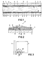
- Figure 1 is a sectional view of a part of a display device 1 having two supporting plates 2 and 3 between which a liquid crystal 4 is present.
- the inner surfaces of the supporting plates 2 and 3 have electrically and chemically insulating layers 5.
- a large number of picture electrodes 6 and 7 arranged respectively in rows and columns are provided on the supporting plates 2 and 3, respectively.
- the oppositely located picture electrodes 6 and 7 form the picture elements of the display device.
- Strip-shaped column electrodes 11 are provided between the columns of picture electrodes 7.
- the column electrodes 11 and the picture electrodes 7 can advantageously be integrated to strip-shaped electrodes.
- Strip-shaped row electrodes 8 are provided between the rows of picture electrodes 6.
- Each picture electrode 6 is connected to a row electrode 8 by means of a switching element 9 shown diagrammatically.
- the switching elements 9 give the liquid crystal 4 a sufficiently steep threshold with respect to the applied voltage and give the liquid crystal 4 a memory.
- Liquid crystal-orienting layers 10 are furthermore provided on the inner surfaces of the supporting plates 2 and 3. As is known, another orientation condition of the liquid crystal molecules and therewith an optically different condition can be obtained by applying a voltage across the liquid crystal layer 4.
- the display device can be realized both as a transmissive and as a reflective device.
- FIG 2 is a sectional view of a first embodiment of the switching elements 9 shown diagrammatically in Figure 1, in which like components are referred to by like reference numerals.
- a 0,2/um thick electrically and chemically insulating layer 5 of silicon nitride is provided on the supporting plate 2.
- a 1 ⁇ m thick layer of preferably already p-doped polysilicon is then provided on the layer 5, in which former layer polysilicon islands 20 are formed by means of a photolithographic process. If the starting material is undoped polysilicon, a p-doping is provided in the islands, for example by ion implantation of boron, to give an active doping concentration of 1 x 10 15 /cm 3 .
- a mask is provided on the polysilicon islands 20 by means of a photolithographic process for providing in the regions 22 and 23 and n + doping, for example by ion implantation of phosphorus, to give an active doping concentration of 1 x 10 18 /cm 3 .
- n + doping By providing the n + doping, a flat n + -pn + structure is formed in the islands 20.
- the assembly is then annealed for 1 hour at a maximum temperature of 1,000°C.
- a 0,2 ⁇ m thick covering layer 24 of silicon oxide or silicon nitride is then provided over the p-doped region 21 and partly over the n +- doped regions 22 and 23.
- the picture electrodes 6 and the row electrodes 8 of indium oxide and/or tin oxide are then provided in a thickness of 0.15 ⁇ m in such manner that a picture electrode 6 covers the exposed surface of the n+-doped region 22 and a raw electrode 8 covers the exposed surface of the n + -doped region 23.
- a 0.1 ⁇ m thick orienting layer 10 of a polyimide is then provided over the whole structure.
- Figure 3 is a plan view of the structure shown in Figure 2.
- the surface area of the picture electrodes is approximately 250 x 250 ⁇ m 2 .
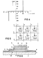
- Figure 4 shows the current voltage characteristic of the described switching element with the said doping concentrations.
- V pt the voltage V is substantially independent of the current I, so that the series resistance of the switching element is negligibly small. This is the result of the very small width d of the p-doped region 21.
- the depletion layer of the reverse biased p-n junction expands to a greater extent in the region 21 than the depletion layer of the forward biased p-n junction decreases in the region.
- the two depletion layers melt each other and overlap each other, respectively, before breakdown occurs.
- the characteristic is completely symmetrical, which is desirable because the display device is operated with alternating voltage so as to prevent undesired electrode processes by direct voltage drive.
- the value of the punch-through voltage V pt which is independent of the dimensions a and b of the switching element, can be adjusted by means of the doping concentrations and the width d of the region 21. The occurring reverse current can be minimized by suitable choice of the width b and the thickness of the switching elements.
- the driving of the display device will be described in greater detail with reference to Figure 5.
- the picture elements formed by the picture electrodes 6 and 7 are connected between the row electrodes 8 and the column electrodes 11, a switching element 9 being connected in series with each picture element.
- the row electrodes 8 are driven by voltage pulses +V s .
- voltage pulses -V d are applied to selected column electrodes 11.
- a voltage difference V s +V d then exists across said selected column electrodes 11 and the associated raw electrode 8. This voltage difference also exists across the series arrangement of the picture elements and the switching elements 9.
- the voltage difference V s +V d is larger than the threshold voltage Vpt of the switching elements 9.
- V s + V d As a result of this a part of the voltage difference V s + V d comes across the driven picture elements, which is sufficient to bring the liquid crystal 4 at the area of the picture elements to a different orientation condition.
- Voltage pulses +V d are applied to the non- selected column electrodes 11. A voltage difference V s - V d then exists across said column electrodes 11 and the row electrodes 8. This voltage difference Vs - V d is smaller than the threshold voltage V pt of the switching elements so that they are not energized.
- the voltage pulses ⁇ V d are smaller than the threshold voltage V pt of the switching elements 9. This prevents information being written in picture elements of non-driven row electrodes 8. After the information has been written on a driven row electrode 8, the next row electrode 8 is energized.
- both the row electrodes and column electrodes may serve as control electrodes or information electrodes.
- Figure 6 shows a second embodiment of the switching elements 9 shown diagrammatically in Figure 1.
- Like components are referred to by like reference numerals as in Figure 1.
- a 0.2 ⁇ m thick electrically and chemically insulating layer 5 of silicon nitride is provided on the supporting plate 2.
- a 1 ⁇ m thick n + doped layer 30 of polysilicon, a 0.1 to 1 ⁇ m thick p-doped layer 31 of polysilicon and again a 1 ⁇ m thick n + -doped layer 32 of polysilicon are provided successively on the layer 5 by means of chemical vapour-deposition methods.
- the doping concentrations are in the same order of magnitude as in the embodiment described with reference to Figure 2.
- a 0,1 ⁇ m thick covering layer (capping layer) of undoped polysilicon may be provided between the two n + -p junctions.
- a photolithographic process polysilicon islands 20 are formed.
- a mask is then provided photolithographically so as to etch away a part of the polysilicon island 20 and to thus create a contact possibility with the n + -doped layer 30.
- a 0.2 ⁇ m thick capping layer 34 of silicon oxide or silicon nitride is then provided over the whole island 20.
- Contact holes are etched herein photolithographically for the 0.15 ⁇ m thick picture electrodes 6 and row electrodes 8 of indium oxide and/or tin oxide to be provided afterwards, in such manner that the picture electrode 6 covers the exposed surface of the n + -doped region 32 and the row electrode 8 covers the exposed surface of the n + -doped region 30.
- a 0.1 / um thick liquid crystal-orienting layer 35 of a polymer is then provided over the whole structure.
- the stacked n + p-n + structure can also be realized by successively implanting a 2/um thick undoped layer of polysilicon with, for example, phosphorus, boron, and again phosphorus with such an energy that the concentration maxima are sufficiently spaced to form separated n + , p and n + doped regions.
- the switching elements may also be constructed in a p-n-p structure.
- the switching elements may also be used with other display media showing substantially no threshold and/or no intrinsic memory, for example, electrophoretic and electroceramic display media.
Landscapes
- Physics & Mathematics (AREA)
- Engineering & Computer Science (AREA)
- Nonlinear Science (AREA)
- General Physics & Mathematics (AREA)
- Chemical & Material Sciences (AREA)
- Crystallography & Structural Chemistry (AREA)
- Mathematical Physics (AREA)
- Microelectronics & Electronic Packaging (AREA)
- Optics & Photonics (AREA)
- Computer Hardware Design (AREA)
- Theoretical Computer Science (AREA)
- Liquid Crystal (AREA)
- Devices For Indicating Variable Information By Combining Individual Elements (AREA)
- Control Of Indicators Other Than Cathode Ray Tubes (AREA)
Applications Claiming Priority (2)
| Application Number | Priority Date | Filing Date | Title |
|---|---|---|---|
| NL8103376 | 1981-07-16 | ||
| NL8103376A NL8103376A (nl) | 1981-07-16 | 1981-07-16 | Weergeefinrichting. |
Publications (2)
| Publication Number | Publication Date |
|---|---|
| EP0070598A1 true EP0070598A1 (fr) | 1983-01-26 |
| EP0070598B1 EP0070598B1 (fr) | 1987-01-14 |
Family
ID=19837794
Family Applications (1)
| Application Number | Title | Priority Date | Filing Date |
|---|---|---|---|
| EP82200879A Expired EP0070598B1 (fr) | 1981-07-16 | 1982-07-12 | Dispositif d'affichage |
Country Status (8)
| Country | Link |
|---|---|
| US (1) | US4583087A (fr) |
| EP (1) | EP0070598B1 (fr) |
| JP (1) | JPS5818674A (fr) |
| CA (1) | CA1181513A (fr) |
| DE (1) | DE3275142D1 (fr) |
| ES (1) | ES8306278A1 (fr) |
| HK (1) | HK58288A (fr) |
| NL (1) | NL8103376A (fr) |
Cited By (18)
| Publication number | Priority date | Publication date | Assignee | Title |
|---|---|---|---|---|
| FR2551902A1 (fr) * | 1983-09-13 | 1985-03-15 | Thomson Csf | Ecran de visualisation a adressage par elements non lineaires et son procede de fabrication |
| FR2553218A1 (fr) * | 1983-10-07 | 1985-04-12 | Commissariat Energie Atomique | Ecran d'affichage a matrice active sans croisement des lignes et des colonnes d'adressage |
| EP0150728A3 (fr) * | 1984-01-23 | 1986-01-08 | Energy Conversion Devices, Inc. | Dispositifs d'affichage à cristal liquide commandés par des diodes comprenant des alliages amorphes de silicium |
| EP0174431A1 (fr) * | 1984-09-10 | 1986-03-19 | International Business Machines Corporation | Dispositifs d'affichage à cristaux liquides et leur procédé de fabrication |
| FR2579775A1 (fr) * | 1985-04-02 | 1986-10-03 | Thomson Csf | Procede de realisation d'elements de commande non lineaire pour ecran plat de visualisation electro-optique et ecran plat realise selon ce procede |
| GB2173935A (en) * | 1985-04-03 | 1986-10-22 | Gen Electric Plc | Liquid crystal displays |
| FR2581781A1 (fr) * | 1985-05-07 | 1986-11-14 | Thomson Csf | Elements de commande non lineaire pour ecran plat de visualisation electrooptique et son procede de fabrication |
| EP0217469A1 (fr) * | 1985-09-30 | 1987-04-08 | Koninklijke Philips Electronics N.V. | Dispositif d'affichage à commande d'attaque |
| EP0217466A1 (fr) * | 1985-09-30 | 1987-04-08 | Koninklijke Philips Electronics N.V. | Dispositif d'affichage à commande d'attaque |
| EP0223967A1 (fr) * | 1985-10-31 | 1987-06-03 | International Business Machines Corporation | Affichage à cristaux liquides de type matriciel comprenant un transistor en couche mince |
| EP0184341A3 (en) * | 1984-11-12 | 1988-04-20 | Semiconductor Energy Laboratory Co., Ltd. | Liquid crystal display panel and manufacturing method thereof |
| EP0166225A3 (en) * | 1984-06-29 | 1988-07-13 | Energy Conversion Devices, Inc. | High yield liquid crystal display and method of making same |
| EP0289071A1 (fr) * | 1987-04-16 | 1988-11-02 | Philips Electronics Uk Limited | Dispositif d'affichage à cristal liquide |
| WO1989002095A1 (fr) * | 1987-08-27 | 1989-03-09 | Hughes Aircraft Company | Affichages a cristaux liquides mos fabriques avec des tranches de silicium traitees par implantation |
| US4839707A (en) * | 1987-08-27 | 1989-06-13 | Hughes Aircraft Company | LCMOS displays fabricated with implant treated silicon wafers |
| EP0198346A3 (fr) * | 1985-04-08 | 1989-10-18 | Energy Conversion Devices, Inc. | Dispositifs semi-conducteurs à seuil utilisant l'effet de perçage |
| US4929569A (en) * | 1984-01-23 | 1990-05-29 | Ovonic Imaging Systems, Inc. | Method of fabricating amorphous silican diode addressed liquid crystal display |
| US5061040A (en) * | 1984-01-23 | 1991-10-29 | Ois Optical Imaging Systems, Inc. | Liquid crystal displays operated by amorphous silicon alloy diodes |
Families Citing this family (18)
| Publication number | Priority date | Publication date | Assignee | Title |
|---|---|---|---|---|
| JPH0617957B2 (ja) * | 1985-05-15 | 1994-03-09 | セイコー電子工業株式会社 | 液晶表示装置 |
| NL8601373A (nl) * | 1986-05-29 | 1987-12-16 | Philips Nv | Weergeefinrichting met verbeterde aansturing. |
| JP2816549B2 (ja) * | 1986-10-22 | 1998-10-27 | セイコーインスツルメンツ株式会社 | 電気光学装置 |
| NL8701420A (nl) * | 1987-06-18 | 1989-01-16 | Philips Nv | Weergeefinrichting en werkwijze voor het besturen van een dergelijke weergeefinrichting. |
| NL8702494A (nl) * | 1987-10-19 | 1989-05-16 | Vermeulen Hollandia Octrooien | Slingerinrichting. |
| GB2214018A (en) * | 1987-12-23 | 1989-08-23 | Philips Electronic Associated | Current mirror circuit arrangement |
| EP0322860B1 (fr) * | 1987-12-28 | 1996-09-11 | Fuji Electric Co., Ltd. | Dispositif semi-conducteur à grille isolée |
| NL8802409A (nl) * | 1988-09-30 | 1990-04-17 | Philips Nv | Weergeefinrichting, steunplaat voorzien van diode en geschikt voor de weergeefinrichting en werkwijze ter vervaardiging van de steunplaat. |
| NL8802436A (nl) * | 1988-10-05 | 1990-05-01 | Philips Electronics Nv | Werkwijze voor het besturen van een weergeefinrichting. |
| NL8802997A (nl) * | 1988-12-07 | 1990-07-02 | Philips Nv | Weergeefinrichting. |
| US5243452A (en) * | 1991-12-06 | 1993-09-07 | Ncr Corporation | Liquid crystal display with pen-input capability |
| US5610629A (en) * | 1991-12-06 | 1997-03-11 | Ncr Corporation | Pen input to liquid crystal display |
| US5751453A (en) * | 1991-12-06 | 1998-05-12 | Ncr Corporation | Liquid crystal display with pen-input capability |
| US5402145A (en) * | 1993-02-17 | 1995-03-28 | Copytele, Inc. | Electrophoretic display panel with arc driven individual pixels |
| JPH07152049A (ja) * | 1993-11-29 | 1995-06-16 | Sharp Corp | 液晶表示装置およびその製造方法 |
| DE10328377A1 (de) * | 2003-06-24 | 2005-01-20 | Siemens Ag | Elektrochromes Anzeigesystem |
| CN101010793B (zh) * | 2004-06-30 | 2011-09-28 | Nxp股份有限公司 | 制造具有通过纳米线接触的导电材料层的电子器件的方法 |
| US20160313577A1 (en) * | 2015-04-23 | 2016-10-27 | Laxense Inc. | Dual-junction optical modulator and the method to make the same |
Citations (1)
| Publication number | Priority date | Publication date | Assignee | Title |
|---|---|---|---|---|
| US4223308A (en) * | 1979-07-25 | 1980-09-16 | Northern Telecom Limited | LCDs (Liquid crystal displays) controlled by thin film diode switches |
Family Cites Families (13)
| Publication number | Priority date | Publication date | Assignee | Title |
|---|---|---|---|---|
| JPS5135298A (ja) * | 1974-09-20 | 1976-03-25 | Hitachi Ltd | Ekishohyojisochi |
| GB1573309A (en) * | 1976-03-24 | 1980-08-20 | Mullard Ltd | Semiconductor devices and their manufacture |
| NL191683C (nl) * | 1977-02-21 | 1996-02-05 | Zaidan Hojin Handotai Kenkyu | Halfgeleidergeheugenschakeling. |
| JPS53145578A (en) * | 1977-05-25 | 1978-12-18 | Nec Corp | Diode varister |
| NL7801532A (nl) * | 1978-02-10 | 1979-08-14 | Philips Nv | Halfgeleiderinrichting. |
| JPS5559432A (en) * | 1978-10-27 | 1980-05-02 | Dainippon Printing Co Ltd | Electro-optical display panel of matrix type and device thereof |
| US4247915A (en) * | 1979-01-02 | 1981-01-27 | Texas Instruments Incorporated | Punch-through load devices in high density static memory cell |
| US4251136A (en) * | 1979-07-25 | 1981-02-17 | Northern Telecom Limited | LCDs (Liquid crystal displays) controlled by thin film diode switches |
| US4373165A (en) * | 1979-11-07 | 1983-02-08 | Texas Instruments Incorporated | Very high density punch-through read-only-memory |
| JPS5672488A (en) * | 1979-11-19 | 1981-06-16 | Matsushita Electric Industrial Co Ltd | Liquid crystal display unit |
| US4405933A (en) * | 1981-02-04 | 1983-09-20 | Rca Corporation | Protective integrated circuit device utilizing back-to-back zener diodes |
| JPS57130081A (en) * | 1981-02-06 | 1982-08-12 | Matsushita Electric Industrial Co Ltd | Liquid crystal picture display device |
| JPS57190923A (en) * | 1981-05-20 | 1982-11-24 | Seiko Epson Corp | Color liquid crystal display body |
-
1981
- 1981-07-16 NL NL8103376A patent/NL8103376A/nl not_active Application Discontinuation
-
1982
- 1982-07-09 US US06/396,989 patent/US4583087A/en not_active Expired - Fee Related
- 1982-07-12 DE DE8282200879T patent/DE3275142D1/de not_active Expired
- 1982-07-12 EP EP82200879A patent/EP0070598B1/fr not_active Expired
- 1982-07-14 ES ES513951A patent/ES8306278A1/es not_active Expired
- 1982-07-14 JP JP57121363A patent/JPS5818674A/ja active Pending
- 1982-07-15 CA CA000407376A patent/CA1181513A/fr not_active Expired
-
1988
- 1988-08-04 HK HK582/88A patent/HK58288A/xx unknown
Patent Citations (1)
| Publication number | Priority date | Publication date | Assignee | Title |
|---|---|---|---|---|
| US4223308A (en) * | 1979-07-25 | 1980-09-16 | Northern Telecom Limited | LCDs (Liquid crystal displays) controlled by thin film diode switches |
Non-Patent Citations (1)
| Title |
|---|
| NEUES AUS DER TECHNIK, no. 3, 15th June 1981, pages 2,3, Würzburg, (DE) * |
Cited By (26)
| Publication number | Priority date | Publication date | Assignee | Title |
|---|---|---|---|---|
| GB2146827A (en) * | 1983-09-13 | 1985-04-24 | Thomson Csf | Display panels |
| FR2551902A1 (fr) * | 1983-09-13 | 1985-03-15 | Thomson Csf | Ecran de visualisation a adressage par elements non lineaires et son procede de fabrication |
| FR2553218A1 (fr) * | 1983-10-07 | 1985-04-12 | Commissariat Energie Atomique | Ecran d'affichage a matrice active sans croisement des lignes et des colonnes d'adressage |
| EP0145520A3 (en) * | 1983-10-07 | 1985-07-10 | Commissariat A L'energie Atomique Etablissement De Caractere Scientifique Technique Et Industriel | Display screen with active matrix without intersection of the row and column address lines |
| US4694287A (en) * | 1983-10-07 | 1987-09-15 | Commissariat A L'energie Atomique | Active matrix display screen without intersection of the addressing columns and rows |
| EP0150728A3 (fr) * | 1984-01-23 | 1986-01-08 | Energy Conversion Devices, Inc. | Dispositifs d'affichage à cristal liquide commandés par des diodes comprenant des alliages amorphes de silicium |
| US5061040A (en) * | 1984-01-23 | 1991-10-29 | Ois Optical Imaging Systems, Inc. | Liquid crystal displays operated by amorphous silicon alloy diodes |
| US4929569A (en) * | 1984-01-23 | 1990-05-29 | Ovonic Imaging Systems, Inc. | Method of fabricating amorphous silican diode addressed liquid crystal display |
| EP0166225A3 (en) * | 1984-06-29 | 1988-07-13 | Energy Conversion Devices, Inc. | High yield liquid crystal display and method of making same |
| US4662719A (en) * | 1984-09-10 | 1987-05-05 | International Business Machines Corporation | Liquid crystal display and method for production |
| EP0174431A1 (fr) * | 1984-09-10 | 1986-03-19 | International Business Machines Corporation | Dispositifs d'affichage à cristaux liquides et leur procédé de fabrication |
| EP0184341A3 (en) * | 1984-11-12 | 1988-04-20 | Semiconductor Energy Laboratory Co., Ltd. | Liquid crystal display panel and manufacturing method thereof |
| FR2579775A1 (fr) * | 1985-04-02 | 1986-10-03 | Thomson Csf | Procede de realisation d'elements de commande non lineaire pour ecran plat de visualisation electro-optique et ecran plat realise selon ce procede |
| EP0200599A1 (fr) * | 1985-04-02 | 1986-11-05 | Thomson-Csf | Procédé de réalisation d'éléments de commande non linéaire pour écran plat de visualisation électrooptique et écran plat réalisé selon ce procédé |
| US4717244A (en) * | 1985-04-03 | 1988-01-05 | The General Electric Company, P.L.C. | Active matrix addressed liquid crystal display wherein the number of overlap regions of the address line is reduced |
| GB2173935A (en) * | 1985-04-03 | 1986-10-22 | Gen Electric Plc | Liquid crystal displays |
| EP0198346A3 (fr) * | 1985-04-08 | 1989-10-18 | Energy Conversion Devices, Inc. | Dispositifs semi-conducteurs à seuil utilisant l'effet de perçage |
| EP0202150A1 (fr) * | 1985-05-07 | 1986-11-20 | Thomson-Csf | Elément de commande non linéaire pour écran plat de visualisation électrooptique et son procédé de fabrication |
| FR2581781A1 (fr) * | 1985-05-07 | 1986-11-14 | Thomson Csf | Elements de commande non lineaire pour ecran plat de visualisation electrooptique et son procede de fabrication |
| US4810637A (en) * | 1985-05-07 | 1989-03-07 | Thomson-Csf | Non-linear control element for a flat electrooptical display screen and a method of fabrication of said control element |
| EP0217469A1 (fr) * | 1985-09-30 | 1987-04-08 | Koninklijke Philips Electronics N.V. | Dispositif d'affichage à commande d'attaque |
| EP0217466A1 (fr) * | 1985-09-30 | 1987-04-08 | Koninklijke Philips Electronics N.V. | Dispositif d'affichage à commande d'attaque |
| EP0223967A1 (fr) * | 1985-10-31 | 1987-06-03 | International Business Machines Corporation | Affichage à cristaux liquides de type matriciel comprenant un transistor en couche mince |
| EP0289071A1 (fr) * | 1987-04-16 | 1988-11-02 | Philips Electronics Uk Limited | Dispositif d'affichage à cristal liquide |
| US4839707A (en) * | 1987-08-27 | 1989-06-13 | Hughes Aircraft Company | LCMOS displays fabricated with implant treated silicon wafers |
| WO1989002095A1 (fr) * | 1987-08-27 | 1989-03-09 | Hughes Aircraft Company | Affichages a cristaux liquides mos fabriques avec des tranches de silicium traitees par implantation |
Also Published As
| Publication number | Publication date |
|---|---|
| EP0070598B1 (fr) | 1987-01-14 |
| NL8103376A (nl) | 1983-02-16 |
| ES513951A0 (es) | 1983-05-01 |
| JPS5818674A (ja) | 1983-02-03 |
| DE3275142D1 (en) | 1987-02-19 |
| CA1181513A (fr) | 1985-01-22 |
| US4583087A (en) | 1986-04-15 |
| ES8306278A1 (es) | 1983-05-01 |
| HK58288A (en) | 1988-08-12 |
Similar Documents
| Publication | Publication Date | Title |
|---|---|---|
| US4583087A (en) | Matrix display device with diode switching elements | |
| US4251136A (en) | LCDs (Liquid crystal displays) controlled by thin film diode switches | |
| US4413883A (en) | Displays controlled by MIM switches of small capacitance | |
| US4441791A (en) | Deformable mirror light modulator | |
| US7148506B2 (en) | Active matrix display and electrooptical device | |
| US4024626A (en) | Method of making integrated transistor matrix for flat panel liquid crystal display | |
| US4839707A (en) | LCMOS displays fabricated with implant treated silicon wafers | |
| JPH0135352B2 (fr) | ||
| EP0217466B1 (fr) | Dispositif d'affichage à commande d'attaque | |
| EP0442560B1 (fr) | Dispositif d'affichage | |
| GB2212659A (en) | Multi-level circuit cross-overs | |
| US20010045996A1 (en) | Active matrix substrate and producing method of the same | |
| EP0046873A1 (fr) | Modulateur de lumière à miroir déformable | |
| EP0369450A2 (fr) | Circuit de protection d'entrée pour dispositif d'affichage électro-optique | |
| US4952984A (en) | Display device including lateral schottky diodes | |
| US5323254A (en) | Display device with electrostatic discharge protection | |
| JPH05134273A (ja) | デイスプレイスクリーンのためのマトリツクス制御構造及びその製造方法 | |
| US5506165A (en) | Method of manufacturing liquid-crystal display panel | |
| KR100288368B1 (ko) | 박막트랜지스터와이것을제조하기위한방법 | |
| JP2000267137A (ja) | 液晶表示装置 | |
| WO1989002095A1 (fr) | Affichages a cristaux liquides mos fabriques avec des tranches de silicium traitees par implantation | |
| EP0521565B1 (fr) | Dispositif semiconducteur et procédé de fabrication de ce dispositif ainsi que dispositif d'affichage munie d'un tel dispositif semiconducteur | |
| JPH0618929A (ja) | アクティブマトリクス基板の製造方法 | |
| EP0335724A2 (fr) | Riseau de transistor couche mince pour un dispositif électro-optique et procédé pour sa fabrication | |
| JPH0230020B2 (fr) |
Legal Events
| Date | Code | Title | Description |
|---|---|---|---|
| PUAI | Public reference made under article 153(3) epc to a published international application that has entered the european phase |
Free format text: ORIGINAL CODE: 0009012 |
|
| 17P | Request for examination filed |
Effective date: 19820712 |
|
| AK | Designated contracting states |
Designated state(s): CH DE FR GB IT LI |
|
| GRAA | (expected) grant |
Free format text: ORIGINAL CODE: 0009210 |
|
| AK | Designated contracting states |
Kind code of ref document: B1 Designated state(s): CH DE FR GB IT LI |
|
| ITF | It: translation for a ep patent filed | ||
| REF | Corresponds to: |
Ref document number: 3275142 Country of ref document: DE Date of ref document: 19870219 |
|
| ET | Fr: translation filed | ||
| PLBE | No opposition filed within time limit |
Free format text: ORIGINAL CODE: 0009261 |
|
| STAA | Information on the status of an ep patent application or granted ep patent |
Free format text: STATUS: NO OPPOSITION FILED WITHIN TIME LIMIT |
|
| 26N | No opposition filed | ||
| PGFP | Annual fee paid to national office [announced via postgrant information from national office to epo] |
Ref country code: CH Payment date: 19891027 Year of fee payment: 8 |
|
| PG25 | Lapsed in a contracting state [announced via postgrant information from national office to epo] |
Ref country code: LI Effective date: 19900731 Ref country code: CH Effective date: 19900731 |
|
| REG | Reference to a national code |
Ref country code: CH Ref legal event code: PL |
|
| ITTA | It: last paid annual fee | ||
| PGFP | Annual fee paid to national office [announced via postgrant information from national office to epo] |
Ref country code: GB Payment date: 19920630 Year of fee payment: 11 |
|
| PGFP | Annual fee paid to national office [announced via postgrant information from national office to epo] |
Ref country code: FR Payment date: 19920729 Year of fee payment: 11 |
|
| PGFP | Annual fee paid to national office [announced via postgrant information from national office to epo] |
Ref country code: DE Payment date: 19920928 Year of fee payment: 11 |
|
| PG25 | Lapsed in a contracting state [announced via postgrant information from national office to epo] |
Ref country code: GB Effective date: 19930712 |
|
| GBPC | Gb: european patent ceased through non-payment of renewal fee |
Effective date: 19930712 |
|
| PG25 | Lapsed in a contracting state [announced via postgrant information from national office to epo] |
Ref country code: FR Effective date: 19940331 |
|
| PG25 | Lapsed in a contracting state [announced via postgrant information from national office to epo] |
Ref country code: DE Effective date: 19940401 |
|
| REG | Reference to a national code |
Ref country code: FR Ref legal event code: ST |