EP0071296A1 - Bürosystem mit Datenendgeräte, einem Datenverarbeiter und Nebengeräte und Schaltvorrichtung zum Massdatentransport zwischen den Nebengeräten und Schaltvorrichtung zur Benutzung in einem solchen Bürosystem - Google Patents
Bürosystem mit Datenendgeräte, einem Datenverarbeiter und Nebengeräte und Schaltvorrichtung zum Massdatentransport zwischen den Nebengeräten und Schaltvorrichtung zur Benutzung in einem solchen Bürosystem Download PDFInfo
- Publication number
- EP0071296A1 EP0071296A1 EP82200912A EP82200912A EP0071296A1 EP 0071296 A1 EP0071296 A1 EP 0071296A1 EP 82200912 A EP82200912 A EP 82200912A EP 82200912 A EP82200912 A EP 82200912A EP 0071296 A1 EP0071296 A1 EP 0071296A1
- Authority
- EP
- European Patent Office
- Prior art keywords
- data
- connection
- switching
- switching module
- auxiliary
- Prior art date
- Legal status (The legal status is an assumption and is not a legal conclusion. Google has not performed a legal analysis and makes no representation as to the accuracy of the status listed.)
- Granted
Links
Images


Classifications
-
- G—PHYSICS
- G06—COMPUTING OR CALCULATING; COUNTING
- G06F—ELECTRIC DIGITAL DATA PROCESSING
- G06F13/00—Interconnection of, or transfer of information or other signals between, memories, input/output devices or central processing units
- G06F13/38—Information transfer, e.g. on bus
- G06F13/40—Bus structure
- G06F13/4004—Coupling between buses
- G06F13/4022—Coupling between buses using switching circuits, e.g. switching matrix, connection or expansion network
-
- G—PHYSICS
- G06—COMPUTING OR CALCULATING; COUNTING
- G06Q—INFORMATION AND COMMUNICATION TECHNOLOGY [ICT] SPECIALLY ADAPTED FOR ADMINISTRATIVE, COMMERCIAL, FINANCIAL, MANAGERIAL OR SUPERVISORY PURPOSES; SYSTEMS OR METHODS SPECIALLY ADAPTED FOR ADMINISTRATIVE, COMMERCIAL, FINANCIAL, MANAGERIAL OR SUPERVISORY PURPOSES, NOT OTHERWISE PROVIDED FOR
- G06Q99/00—Subject matter not provided for in other groups of this subclass
Definitions
- the invention relates to an office system for processing a data file by means of at least two simultaneously operational terminals, common processor means, a first number of peripheral apparatuses, and a data bus which inter connects the processor means, the terminals and the peripheral apparatuses.
- a terminal station customarily comprises a keyboard for the input of alphanumeric data and control signals, a display device for the display of such alphanumeric data, for example 25 lines of 40 characters each, and possibly further elements such as a foreground memory, a (small) processor and an output apparatus such as a character printer, for example a daisy wheel printer.
- the peripheral apparatuses may be constituted by inter alia one or more background memories such as a magnetic disc memory, or a high-speed character printer which comprises, for example, a rotating drum. Systems of this kind are often used and offer good results when used for the processing and filing of text matter consisting of alphanumeric characters which are organized in lines and have fixed shapes.
- the characters may be, for example, matrix characters having a standard format of 7 x 9 dots.
- the set of characters may also be extended by means of so-called graphic characters so that the text can be elucidated with figures to a given extent.
- the object in accordance with the invention is achieved in that for the updating of a document file and for mass data transport between a second number of auxiliary apparatuses, that is to say between at least:
- each switching module When use is made of a third number of n internal data highways, the third connection in each switching module preferably comprises n lines, each of which is coupled to a respective internal data highway, each switching module preferably having n second states for performing a 1-cut-of-n selection from said n lines.
- the internal data highway itself may thus have a very simple construction and the selection function may thus be present within the switching module.
- the mass data transport can then be monitored and synchronized by the auxiliary apparatuses themselves.
- an auxiliary station itself can interrupt or terminate the mass data transport, if desired.
- the memory device comprising a digital video disc
- a storage device having k separate storage positions and a common loading position for the memory device and the storage device, there being provided a selection/transport device for transporting a selectable video disc between the associated storage position and the loading position, said storage device comprising a second control member which is connected to said data bus as a further peripheral apparatus.
- control member thereof When the control member thereof is constructed as a peripheral apparatus of the data bus/processor means, an attractive separation is made between the electromechanical selection of the amount of data to be transported and the actual mass data transport; during the electromechanical selection only a limited number of instructions need to be transported; this can be readily realized via the data bus. It has also been found that an attractive modular construction of the memory device comprising video discs can thus be realized. After all, the electromechanical selection and presentation of a video disc from a storage position is very slow in comparison with the electronic/electromechanical selection of a data block on a video disc; this consideration also favours the construction of the control member as a peripheral apparatus.
- the invention also relates to a switching device for use in an office system of the described kind in which there are provided at least six correspondingly constructed switching modules.
- the internal construction of the switching module may thus also be of an attractive modular type.
- Fig. 1 is a block diagram of an example of an office system configuration.
- the central data processing device is formed by a computer 52.
- the computer in this embodiment is a commercially available mini-computer, make N.V.Philips' Gloeilampenfabrieken, Eindhoven, the Netherlands, type P357.
- Minicomputers of another make can alternatively be used, but will not be described herein for the sake of brevity.
- the term "minicomputer" per se and the category of machines characterized thereby are widely used in the data processing industry.
- the computer comprises control (interface) units 58, 60, 62, 64 for peripheral apparatuses, a central processor unit 54, a general processing memory 56, a general purpose data but 67 which interconnects these parts, and a further interface unit 66 for a peripheral apparatus.
- the interface units are shown as blocks; said minicomputer actually comprises connection facilities for peripheral apparatuses, each connection comprising its own channel interface unit.
- the interface unit 64 serves, for example, three terminals which are of the customary type set forth in the preamble.
- the interface unit 62 serves a number of first peripheral apparatuses 74, 76, 78.
- Block 74 is a conventional magnetic disc memory for the storage of program data, intermediate data and user data.
- Block 76 represents a control device for a memory device comprising a number of video discs.
- the video discs In the rest state the video discs are arranged in a corresponding number of storage positions, for example as parallel discs with coincident axes. A number of storage positions can be combined to form a storage module.
- a read means for example in the form of a laser element which scans the surface of the video disc which has already been brought into rotation.
- a write means in the form of a laser element may also be present.
- the path up to the loading position forms part of the peripheral apparatus 76 and the remainder forms part of the auxiliary apparatuses 32/34 as will be explained hereinafter.
- Block 78 represents a further conventional peripheral apparatus, for example a fast printer comprising a rotating drum.
- the computer, the work stations and the peripheral apparatuses 74, 78 are known per se; they do not perse form part of the idea of the invention, but are merely included in the system for realising efficient mass data transport. This will be described in detail hereinafter.
- the block diagram shows, inter alia, a second number of auxiliary apparatuses which are in principle suitable for the processing of data which is related to a document field, inter alia by way of mass data transport between the various auxiliary apparatuses.
- block 20 represents a document reader.
- a document for example having the standard format DIN A4 (21.0 x 29.7 cm) is scanned therein in lines, and the scanning data is converted into a series of black/white indicating bits.
- DIN A4 21.0 x 29.7 cm
- a document field having the standard A4 format then supplies a quantity of data of approximately 4M bits.
- a known one-dimensional or two-dimensional matrix of photodiodes together with a shift register for parallel/series conversion (for example, comprising charge-coupled cells).
- a shift register for parallel/series conversion for example, comprising charge-coupled cells.
- the mechanical aspects of this and other auxiliary apparatuses will not be elaborated upon herein, because only the data transport between the auxiliary apparatus and the data bus 67 is considered to be of relevance.
- the data per pixel may be multivalent per se, and also be processed as such in the office system, but this will not be elaborated upon herein for the sake of simplicity.
- Block 22 represents a word processor of a customary type whereby text can be generated and updated for output.
- the word processor may comprise a character organized printer. The alphanumeric texts and Further control signals can be generated locally.
- Word processors are marketed by several manufacturers and they will not be elaborated upon herein whenever the invention does not specifically relate thereto.
- Block 24 represents an image processor which serves to reduce the redundancy in an image.
- Customary black/white configurations such as those obtained from the document reader 20 contain a substantial redundancy.
- the redundancy can be reduced by means of a given, known code,
- the image processor can reduce the redundancy by coding and can reconstruct the complete 1 : 1 image by decoding.
- the less-redundant image can then be stored (block 32).
- Block 26 represents a read/write memory which is capable of storing the complete data of a document field (for example, an A4 document scanned by the document reader 20) or of a complete image from the image processor 24. It is constructed as a conventional random access memory and has a capacity of 4M bits. Addressing is performed by means of an address counter which is incremented by each transport of an elementary amount of data. In order to reach a very high transport speed on the data bus, such an elementary data amount may comprise more than 8 bits which are then buffered. Between the relevant buffer and the output there is provided a converter for converting between said elementary amount and the byte-serial transport.
- Block 28 represents a display device, for example comprising a cathode ray tube and an associated read write memory for one page.
- the cathode ray tube and the read/ write memory are adapted to the definition with which the document field is scanned by the document reader. It is not essential to display the document with the original format; a given enlargement/reduction is permissible.
- the number of pixels per scanning line and the number of lines per image remain the same. Except for the large number of pixels per image, this is a conventional video display device.
- Block 30 represents a printing unit for the formation of a hard copy on paper or a similar material.
- This copy contains the complete information obtained (in block 20) from the document field scanned, or originating from the image processor 24, the memory 26 or the word processor 22. (If the last can be switched over from the alphanumeric to the graphic mode, for example, a processed image can be provided with an additional text).
- the printing unit may be a customary fascimile printer which utilizes, for example, an electrostatic printing element.
- Block 32 represents a memory device comprising a video disc with optical write and read means for the filing of the total pixel-wise information of a document field. The video disc is driven at a uniform speed and modifications can be introduced into its surface by means of, for example, an optical laser in order to store a bit pattern. These modifications can also be detected by means of a laser.
- the device also comprises an interface unit to the environment and a number of further elements which will be described with reference to fig. 8.
- Block 34 corresponds to block 32, except that data can only be read from this memory device.
- Block 36 is an interface unit for a low-speed data connection to the environment, for example by acoustic coupling to a telephone line: these lines have a transmission capacity of a few kilobauds.
- the block 36 comprises a parallel/series converter, because the data connection is generally serial.
- the transport from/to the environment generally takes place via the memory 26. Because there are several internal data highways, the entire switching device will not be blocked during the execution of such a necessarily slow mass data transport.
- Block 38 is an interface unit for a high-speed data line to the environment which has a capacity of, for example, 48 kbauds. Otherwise the same is applicable as for block 36.
- Each of the auxiliary apparatuses 20 to 38 is connected to the switching device 40 by way of an individual connection. For some of these connections the data traffic is in only one direction, and for others in both directions, as indicated by the arrows. Control signals are always transported in both directions.
- the auxiliary apparatuses can be exchanged and all connections to the switching device are identical (bi-directional data transport possible).
- a different number of auxiliary apparatuses may be present. They may all be present at the same location (office), or they may alternatively be functionally coupled to one or more of the terminals 68, 70, 72 and be located together therewith at a separate location. Such a combination is referred to as a word station.
- the switching device 40 (see hereinafter) still establishes the connections between the auxiliary stations.
- This embodiment includes a separate computer 52.
- the work stations may alternatively have a distributed arithmetic capacity, so that a computer network is concerned.
- the assignment of the data bus can then be realized, for example, by means of a distributed arbitration mechanism.
- the data bus then directly connects the terminals, peripheral apparatuses and switching device.
- auxiliary apparatuses are directly connected, via the switching device 40, totheir own connection in the computer (blocks 58 and 60).
- the switching device comprises a number of internal data highways, only two of which (42, 44) are shown for the sake of simplicity.
- a rhombic figure is shown at each crossing of the internal data highways and the connections to the auxiliary stations 20 to 38. This figure symbolizes an organization where a switch which is capable of separating and interconnecting two crossing connections is quasi present.
- mass data transport may be realized between two pairs of auxiliary apparatuses by way of a respective internal data highway.
- the transport may be, for example, from the document reader 20 to the display device 28 and from the read/write memory 26 to the video disc memory device 32.
- the switching device 40 comprises a micro-computer 50 which exchanges control signals with the interface unit 66 of the computer 52.
- the microcomputer controls and realizes the data exchange inter alia by establishing and interrupting the connections between pairs of auxiliary stations via the internal data highways of the switching device.
- Fig. 2 is a block diagram of the switching device.
- the microcomputer 50 comprises a connection 100 to the computer 52.
- An interface protocol V24 according to the CCITT standard is defined on this connection. This is a bit serial operation.
- Another, similar possibility is the IEEE protocol EIA.RS.232.C described in John Conway, "Serial 1/0 thursts Indecomp into Asynchronous Communications", Electronic Design New, August 20, 1978, pages 89-96.
- the former protocol has been selected as the standard for communication between the computer 52 and the microcomputer 50, and also between the computer 52 and peripheral apparatuses 74, 76, 78 and terminals 68, 70, 72.
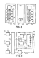
- the microcomputer is constructed in accordance with the block diagram of fig. 9 which will be described first. The figure comprises the following parts:
- the switching device also comprises a mains supply apparatus 102 (shown only symbolically) and the actual internal data highways whose cabling is symbolized by block 105 which contains the switching electronics.
- a switching module 106 (SWCO ... SWCF).
- the line 108 of the switching module SWCO is intended for connection to the associated auxiliary apparatus and the line 110 is intended for connection to the computer 52.
- Each of these lines has a width of 15 bits, that is to say 8 data bits and 7 control bits.
- the switching module SWCO is connected to the microcomputer 50. To this end, the line 112 has a width of 8 bits, as will be explained hereinafter.
- terminating elements 118, 120 are also connected thereto; this implies a line having a width of (6x10) bits to each.
- the communication on the lines 103 etc. takes place via a byte-serial protocol.
- the procedure is as follows. If no mass data transport is required between the auxiliary apparatuses, the lines corresponding to 108 and 110 are interconnected in each switching modules.
- the auxiliary apparatuses (20 to 38 in fig. 1) then operate as if they were peripheral apparatuses of the computer, such as the peripheral apparatus 74, 78.
- the difference between peripheral apparatuses and auxiliary apparatuses is mainly an organizational difference in that only the auxiliary apparatuses are directly connected to the internal data highways of the switching device.
- a given technical realization of an apparatus can be used as an auxiliary apparatus as well as be connected as a peripheral apparatus.
- the computer 52 can supply such a signal on the line 100 that the control of the byte-serial protocol on the line 108 (or a corresponding line in another switching module) is taken over by the microcomputer 50 (by way of the line 112).
- mass data transports can be realized between six pairs of auxiliary apparatuses (SWCO ... SWCF) simultaneously. In as far as it is permitted by the nature of the auxiliary apparatuses, the data transport can be realized in both directions.
- the microcomputer 50 also receives the status signals of the switching electronics in the block 105, so that the progress of (any) mass data transport is also known. If necessary, these status signals are applied to the computer 52.
- the termination elements 118, 120 comprise two resistors for each bit line.
- the bit line is connected to a potential of +5 volts via a resistor of 220 ohms, and to ground potential via a resistor of 330 ohms.
- Fig. 2 shows a solution for increasing this number by utilizing a second switching device DAS' which comprises the same components as the switching device DAS, be it that these components are shown differentiated by means of an accent.
- the corresponding switching modules are interconnected: the connection 108, originally intended for the auxiliary apparatus, is connected to connection 111 of the switching module SWCO' which was originally intended for connection to the computer.
- the connection 110 remains reserved for the computer.
- the second connection 109 of the switching module SWCO' is now reserved for the peripheral apparatus.
- the control connection 131 of the switching electronics MPE' is connected to the data line, together with the control connection 100.
- the connections 108 and 111 are thus dissimilar.
- connections 109 and 110 it is alternatively possible for the connections 109 and 110 to be interconnected so that the connections 108 and 111 remain available for connection to the peripheral apparatus and the computer, respectively.
- the connection pattern between the switching modules need not always be the same; for example, the switching module SWCO can be connected directly to the computer, and the switching module SWC1 directly to a peripheral apparatus. Given pairs of switching modules may also remain non-interconnected; the number of feasible connection directions for an auxiliary apparatus can thus be restricted. All switching devices used need not necessarily have the same number of internal data highways.
- the number of auxiliary apparatuses to be connected can also be increased by interconnection of the internal data highways thereof (block 104).
- Fig. 3 shows a block diagram of one of the identical switching modules SWC (0 ... F) in the switching device.
- the control connection 112 to the microcomputer 50 has a width of 7+1 bits.
- an interface circuit 130 which exchanges secondary control signals with the other parts of the switching module (lines 132); this interface circuit consists of buffer circuits of the type HEF 40097, make N.V.Philips' Gloeilampenfabrieken, Eindhoven, the Netherlands.
- the switching module SWC is furthermore connected to the bidirectional data bus 116 by way of four connection elements which are unidirectionally active.
- a receiver 124 for byte-serial data (each time having a width of 8 bits) and a transmitter 122 for byte-serial data.
- a transmitter 126 and a receiver 128 for control signals are provided.
- the transmitters 122, 126 are activated by channel selectors 132, 134 which each time open up one of the internal data highways by means of a six-bit signal.
- Such a six bit signal has, for example, at the most a single "1" bit which bit unblocks the AND-gate which is provided per bit line for the relevant assigned internal data highway.
- this six bit signal has 8 blocking effects.
- both channel selectors 132, 134 activate; in the receive condition, only the channel selector 134 activates.
- the channel selectors receive, for example, a three-bit signal which indicates the internal data highway by decoding; this three-bit signal is supplied by the element 130.
- the receivers 124, 128 conduct their six-fold input signals which are received on 6x8 and 6x2 lines, respectively.
- Element 136 is a eight-fold 7-to-1 multiplexer which conducts at the most one of the received signals having a width of one byte.
- the control signal therefor is supplied to its input 140 by the element 130.
- element 138 is a double 6-to-1 multiplexer fed with a control signal on its input 142.
- the adaptation of the switching module to the computer 52 is realized by means of an interface element 144. Between the interior of the switching module and the interface element there are provided two unidirectionally active 8-bit data lines 146, 148 and one bidirectional control line 150 (5 bits in the one, 2 bits in the other direction). Line 148 is connected to the multiplexer 136.
- the adaptation of the switching module to the auxiliary apparatuses to be connected is realized by means of an interface element 152.
- Two unidirectional 8-bit data lines 146/154 and 156 and one control line 158 are connected between the interface element and the interior of the switching module, said lines being organized in the same manner as the line 150.
- Lines 146/154 are connected to the transmitter 122 as well as to the interface unit 144.
- Line 156 originates from multiplexer 140.
- the interface elements 144, 152 also receive control signals from the element 130 on the relevant inputs 162, 160.
- Element 164 is a control selector with two states which are selected by a signal on input 165 from element 130.
- Control line 158 can thus be selectively coupled to either the line 150 which is coupled to the interface unit 144 or to the control line 168.
- the control lines 168 (width 7 bits) is coupled, together with the 2-bit control lines 170, 172, to a data flow control element 174.
- a local oscillator 180 In order to supply the latter element with clock pulses there is provided a local oscillator 180.
- the data flow control element 174 exchanges control signals with the element 130 via lines 176/178 as will be explained hereinafter.
- the switching module SWC has two clearly distinct modes of operation.
- the control selector 164 is in the lower state, so that the switching module between the seven control-bit lines of the lines 108 and 110 is transparent.
- the data transmission takes place in one direction directly from the interface unit 152 to the interface unit 144, and in the other direction via the line 148, the multiplexer 136, and the line 156.
- the switching module is thus also transparent for the data lines.
- a data transport is performed, notably a mass data transport, via one of the internal data highways which are symbolized by the block 104 (fig.
- control bypasses the computer 52 because the control selector 164 is in the upper state; control is now effected by means of the data flow control element 174 via the lines 168 and 170 and 172.
- the data transport then takes plate in one direction via the line 154, and via the multiplexer 136 and the line 156 in the other direction.
- a two-wire handshake is realized in this case on the internal data highway via the lines 170 and 172.
- Fig. 4 shows part of the switching module, notably the part which relates to the interaction between the data flow control element 174, the control selector 164 and the control sections of the interface elements 144 and 152, in more detail.
- the control section of the interface element 152 for the auxiliary apparatuses (line 108 in fig. 3).
- the gates in the output direction, such as the gate 220, are of the make Texas Instruments, type 74 LS 38; open collector drive elements.
- the input gates (for example gate 221) are also Texas Instruments type 74132.
- the control section of the interface element 144 for the computer (line 110).
- the elements which are shown as NAND-gates are of the type 74 LS 00.
- the signal indications have the following meaning:
- AND-gate 222 of the type 74 LS 08 controls the operating mode (control selector 164 in fig. 3). If this gate outputs a "O", the data control element 174 controls a mass data transport via one of the internal data highways of the switching device; the signals CM and CL are then blocked. A logic "1" from the gate 222 connects the auxiliary apparatus to the computer. If this "1" is present, the output signal of the inverter 224 (type 74 LS 04) blocks the gates 226, 228. The signals CL , CM are not used for the execution of a mass data transport; during such a transport they are blocked.
- the signals DM and RD are not applied to the computer in the case of a mass data transport; in the other case the gates 226, 228 are blocked.
- the signals RE , IN , TR are applied to the selector switch 230 of the control selector 164 (type 74157).
- the remainder of fig. 4 includes the local oscillator (180 in fig. 3) which comprises a 20 MHz crystal 232 which constitutes a fed-back resonant circuit in conjunction with a resistor 234 (120 Ohms) and some inverters. Also present are a number of gates and sequentially operating logic elements for establishing the correct time relationships between the various signals.
- Element 236 is a clocked set/ruset (RS) flipflop of the type 74 LS 74 which continuously receives a signal +V on its data input. Its inverted output carries a signal ACT which is applied to the microcomputer (line 12 in fig. 3) and to the selector switch 230.
- RS clocked set/ruset
- Its non-inverted output is connected, via an AND-gate, to the selector switch 230 and to a shift register 238.
- Its clock pulse input receives the signal ST from the microcomputer.
- Its reset input receives the signal BR from the microcomputer via an AND-gate, and also a coincidence signalization of the signals DM and RD from the auxiliary apparatus.
- Element 238 is a shift register of the type 74 LS 164 which can receive the signal DM on its data inputs. Its MR (reset) input is connected in parallel with that input of the selector switch 230 which is for the signal TR for the auxiliary station. The shift register is clocked by the local oscillator. A signal DMR which will be described hereinafter is formed by AND-gate 246. Furthermore, a logic function of the output signals Q1, Q2 is applied to the elements 240, 242.
- the element 240 corresponds to the element 236.
- the inverted output thereof is combined in the NAND-gate 248 with the signal TRR which is produced by the handshake on the internal data highway of the switching device.
- the element 242 corresponds to the element 240. Its output signal TRS forms the other synchronization signal of the two-wire handshake on the internal data highway of the switching device.
- the element 244 corresponds to the element 238.
- the clock input receives the signal from the local oscillator. Its data inputs receive the signal DMS and its Mr input receives the signal +V. It stwo outputs Q1, Q2 are combined in the Nand-gate 250. One input thereof is shown provided with a circle which symbolizes an inverter (74 LS 04) which is itself not shown.
- the circuit also comprises the following external connections:
- Fig. 5 is a detailed diagram of a second part of the switching module which section concerns the synchronization signals, including the elements DRI2 (126), REC2 (128), CHSEL2 (134) and MUX2 (138) of fig. 2.
- Block 254 represents a decoder/demultiplexer of the type 74 LS 138. The selection is realized by three address bits ADR received from the microcomputer. In this embodiment only six of the eight feasible codes are used,one for each of the six internal data highways of the switching device. Its connection E3 (enable) is connected to the supply voltage and its inverting input E2 to ground. Its inverting input E1 receives the signal ER in parallel with the circuit of fig. 4.
- the auxiliary apparatus of the relevant switching module can be activated as a data receiver.
- the data output "O" of block 254 in fig. 5 forms a connection to the input 252 in fig. 4.
- the upper half and the lower half of fig. 5 consist of mutually corresponding parts.
- the data output "O" of block 255 is connected to input P10 in fig. 4. Signals on the latter two data outputs set the switching module to the transparent mode of operation between the computer and the auxiliary apparatus.
- Each of the data outputs 1 to 6 of the blocks 254, 255 controls one of the six internal data highways of the switching device (always only one of the two is active: when the auxiliary apparatus acts as a transmitter, the signals TRS and DMS maintain the handshake; when the auxiliary apparatus acts as a data receiver, however, the signals TRR and DMR maintain the handshake.
- the data outputs "7" of the blocks 254, 255 are not used.
- the block 256 is a buffer/gate element. For each input it comprises an inverter and a NAND-gate connected in series. The six XAND-gates can be selectively made conductive for the time-dependent signal DMR by one of the output signals of the block 254. Similarly, the signal TRS can be selectively conducted in the block 263.
- Block 261 is a data selector/multiplexer of the type 74 LS 151 (like block 260). Its selection inputs SO, S1, S2 are connected in parallel with the address bit inputs of the block 254. Its input E is connected in parallel with the enable input E1 of the block 254. Its data input Io is not used and is grounded. Its data inputs I1 ... I6 receive the signals TR1 ... TR6 from the relevant internal data highways. Its data output Y carries said signal TRR.
- the block 260 is connected in substantially the same way as the block 261.
- its enable signal E is derived from the signal ES (which also acts similarly for the block 255 and which is generated by the microcomputer on the connection P8).
- This signal enables a transmission operation for the auxiliary apparatus of the relevant switching module.
- Its data inputs I1 to I6 receive the signals DM1 ... DM6 which originate from the block 256.
- Its data output carries the signal DMS which can be applied to the blocks 244 in fig. 4.
- the blocks 2 5 4, 261 are activated (receiver state) or the blocks 255, 260 are activated (transmitter state), or none of these blocks are activated.
- the output lines DM1 ... 6, TR1 ... 6 thus act in both directions.
- Fig. 6 is a detailed diagram of a third section of the switching module, which section concerns the data signals, notably the elements DRI1 (122), REC1 (124), CHSEL1 (132) and MUX1 (136) in fig. 3.
- the data path has a width of only four bits (instead of 8 bits) and that the switching device comprises only two parallel-connected internal data highways (addressed by three address bits).
- the elements 300, 302 form the interface elements for the auxiliary apparatuses and the computer, respectively (four bits bidirectionally). These elements are quadruple line receivers/blockable line drivers of the type 8T38, make Signetcs, Sunnyvale, CAL., USA. Driving is realized by the signals on P15 and P14, respectively.
- the data received by the element 300 can be stored in a latch circuit of the type 74 LS 75 (block 304) under the control of the signal P9.
- the latch circuit is connected to two buffer circuits 306, 308 (quadruple output stage 74 LS 38, one buffer circuit being provided for each internal data highway.
- the buffer circuits are activated by an element 310 of the type 74 LS 138, each relevant output of which is followed by an inverter.
- This element receives three address bits and the transmission enable signal ES .
- Output line “0" carries the signal P10, and each of the output lines 1 ... 6 addresses one of the internal data highways. Connection of these output lines to a NAND-gate, together with the signal TRS, produces the signals TR1, TR2 (cf. fig. 5). Data is received from the internal data highways via 4 x 2 NAND-gates 312 of the type 8T 37; the other input of each of these gates is grounded. There are provided four selectors 314 ... 320 which receive the signal ER as their enable signal, and also receive the three-bit address for the internal data highway (or the address "0" for the computer). A further data bit can thus be received each time from the element 302 at the input Io. The output data can be applied to the element 300.
- Fig. 7 is a time diagram of a number of signals in a switching module: a mass data transport is initiated between two auxiliary apparatuses.
- the upper twelve signals concern the transmitting auxiliary apparatus, and the lower twelve signals concern the receiving auxiliary apparatus of these signals, ER, ES, AO, A1, A2, ST and BR are supplied by the microcomputer.
- the last two signals concern the synchronization handshake on the internal data highway during the mass data transport.
- Each of the two auxiliary apparatuses comprises its own switching module.
- the start signal is formed to activate the flipflop 236 in fig. 4, the active state thereof being signalled back (signal ACT ) to the microcomputer.
- the signal IN becomes high for the auxiliary apparatus, so that this apparatus is addressed.
- the transmitting auxiliary apparatus is addressed in the same way by means of the same address for the internal data Ihighway.
- the signals IN as well as RE then become high.
- the signal TR becomes active via the flipflop 240 in fig. 4 whereby the handshake is started as indicated by the arrows.
- a series of three data bytes is transported.
- the transmitting auxiliary apparatus forms an active signal RD .
- the transmitting auxiliary apparatus is then deactivated first and subsequently also the receiving auxiliary apparatus.
- the signal TRR proceeds directly to the auxiliary apparatus via the gate 248 and the selector switch 230.
- the signal DM is returned directly (shift register 238 introduces only a small delay), the positions of the flipflops remaining unchanged).
- the two-byte message may also be:
- Block 400 represents, partly symbolically, the general set-up of an auxiliary apparatus.
- Arrow 406 represents the connection to the switching device: 8-bit data path + seven control lines for the signals CM, CL, IN, TR, DM, RD, RE (lines 8 to 12 in fig. 7).
- Block 410 represents an interface element between this connection and the internal data highway of the auxiliary apparatus.
- Block 412 represents internal data processor means, such as a microprocessor.
- Block 414 represents a random access rad/write memory.
- Block 416 is an interface unit between the data bus 408 and the actual functions of the auxiliary apparatus in block 418.
- electromechanical transducers such as actuators and detectors, for example for control signals for addressing the track of a disc memory and detection signals which indicate that the relevant track has indeed been reached.
- the microprocessor may be, for example, a Signetics 2650 or a Zilog Z80, and the modules 410, 414, 416 may be standard components which are compatible therewith.
- the data flow from the auxiliary apparatus can also take place via the data bus and the connection 406.
- auxiliary apparatuses such as word processors can be constructed.
- Fig. 8 notably shows the organization of an auxiliary apparatus which includes a video disc for digital optical recording (D.O.R.).
- the control/detection function in block 418 then concerns:
- block 400 it is detected in block 400 whether the correct sector position has been addressed (sector selection according to section number) one whether this position contains permissible information (for a read operation) or is empty (in the case of a write operation).
- the block 400 is symbolized in fig. 1 by the blocks 32, 34, each of which may comprise such a control unit.
- Block 404 controls a storage module for 64 video discs in order to present a video disc addressed by the computer from a storage position to a transfer position. Moreover, a video disc presented to a second input transfer position can be transported to the former output transfer position.
- the control unit can thus perform inter alia the following functions:
- the storage modules can be linked by making the output transfer position of a storage module coincide with the input transfer position of a next module.
- the block 402 controls a transport module.
- a transport module comprises one (or possible more) input positions which coincide with the output transfer position of a storage module. Furthermore it comprises one or more loading positions which coincide with a corresponding loading position of the actual auxiliary apparatus (block 400). A modular construction of the device is thus also possible.
- the blocks 402, 404 form direct peripheral apparatuses of the computer.
- a video disc can thus be transported to the operational position or to the storage position without the switching device being loaded thereby. This results in a more flexible organisation.
Landscapes
- Engineering & Computer Science (AREA)
- Physics & Mathematics (AREA)
- Theoretical Computer Science (AREA)
- General Physics & Mathematics (AREA)
- General Engineering & Computer Science (AREA)
- General Business, Economics & Management (AREA)
- Computer Hardware Design (AREA)
- Business, Economics & Management (AREA)
- Mathematical Physics (AREA)
- Bus Control (AREA)
- Information Transfer Systems (AREA)
- Communication Control (AREA)
- Exchange Systems With Centralized Control (AREA)
- Document Processing Apparatus (AREA)
- Multi Processors (AREA)
- Small-Scale Networks (AREA)
- Computer And Data Communications (AREA)
Priority Applications (1)
| Application Number | Priority Date | Filing Date | Title |
|---|---|---|---|
| AT82200912T ATE19833T1 (de) | 1981-07-23 | 1982-07-16 | Buerosystem mit datenendgeraete, einem datenverarbeiter und nebengeraete und schaltvorrichtung zum massdatentransport zwischen den nebengeraeten und schaltvorrichtung zur benutzung in einem solchen buerosystem. |
Applications Claiming Priority (2)
| Application Number | Priority Date | Filing Date | Title |
|---|---|---|---|
| NL8103477A NL8103477A (nl) | 1981-07-23 | 1981-07-23 | Kantoorsysteem met eindstations, een dataverwerkende processor en hulpapparaten en een doorschakelinrichting voor het verzorgen van massaal datatransport tussen de hulpapparaten. |
| NL8103477 | 1981-07-23 |
Publications (2)
| Publication Number | Publication Date |
|---|---|
| EP0071296A1 true EP0071296A1 (de) | 1983-02-09 |
| EP0071296B1 EP0071296B1 (de) | 1986-05-14 |
Family
ID=19837837
Family Applications (1)
| Application Number | Title | Priority Date | Filing Date |
|---|---|---|---|
| EP82200912A Expired EP0071296B1 (de) | 1981-07-23 | 1982-07-16 | Bürosystem mit Datenendgeräte, einem Datenverarbeiter und Nebengeräte und Schaltvorrichtung zum Massdatentransport zwischen den Nebengeräten und Schaltvorrichtung zur Benutzung in einem solchen Bürosystem |
Country Status (7)
| Country | Link |
|---|---|
| US (1) | US4464733A (de) |
| EP (1) | EP0071296B1 (de) |
| JP (1) | JPS5824928A (de) |
| AT (1) | ATE19833T1 (de) |
| CA (1) | CA1188816A (de) |
| DE (1) | DE3271135D1 (de) |
| NL (1) | NL8103477A (de) |
Cited By (2)
| Publication number | Priority date | Publication date | Assignee | Title |
|---|---|---|---|---|
| EP0507381A3 (en) * | 1991-04-02 | 1993-09-01 | N.V. Philips' Gloeilampenfabrieken | Method of processing control instruction |
| EP0601382A1 (de) * | 1992-11-23 | 1994-06-15 | Brooktree Corporation | Erweiterbarer, digitaler Multiplexer hoher Schaltgeschwindigkeit |
Families Citing this family (16)
| Publication number | Priority date | Publication date | Assignee | Title |
|---|---|---|---|---|
| JPS5781670A (en) * | 1980-11-07 | 1982-05-21 | Hitachi Ltd | Editing method of document |
| JPS58220293A (ja) * | 1982-06-15 | 1983-12-21 | Nec Corp | 記憶装置 |
| US5129061A (en) * | 1982-11-10 | 1992-07-07 | Wang Laboratories, Inc. | Composite document accessing and processing terminal with graphic and text data buffers |
| US4587633A (en) * | 1982-11-10 | 1986-05-06 | Wang Laboratories, Inc. | Management communication terminal system |
| JPS59200339A (ja) * | 1983-04-27 | 1984-11-13 | Hitachi Ltd | 表示装置 |
| JPS6139186A (ja) * | 1984-07-31 | 1986-02-25 | 株式会社日立製作所 | 自動取引装置 |
| US5062076A (en) * | 1985-07-12 | 1991-10-29 | Wang Laboratories, Inc. | Cascadable, high-bandwidth, multi-channel image transfer controller |
| JPH0827854B2 (ja) * | 1986-06-25 | 1996-03-21 | 株式会社日立製作所 | 取引記録方法 |
| US4855842A (en) * | 1987-08-06 | 1989-08-08 | Professional Training Systems, Inc. | Dedicated programmable controller for interactive video disc system |
| US5140675A (en) * | 1987-10-30 | 1992-08-18 | Canon Kabushiki Kaisha | Printer controller apparatus interfacing with external data sources |
| US5046027A (en) * | 1988-11-08 | 1991-09-03 | Massachusetts General Hospital | Apparatus and method for processing and displaying images in a digital procesor based system |
| US5039847A (en) * | 1989-03-24 | 1991-08-13 | Omron Corporation | Image processing apparatus having an image scanner |
| US5668957A (en) * | 1995-11-02 | 1997-09-16 | International Business Machines Corporation | Method and apparatus for providing virtual DMA capability on an adapter connected to a computer system bus with no DMA support |
| US5771395A (en) * | 1996-04-22 | 1998-06-23 | Lockheed Martin Corporation | System for processing information from scanned documents using event driven interface with patterns loaded in RAM and with address generator for addressing bit patterns |
| US5778172A (en) * | 1996-04-22 | 1998-07-07 | Lockheed Martin Corporation | Enhanced real-time topology analysis system or high speed networks |
| US5872642A (en) * | 1996-04-22 | 1999-02-16 | Lockheed Martin Corporation | System for transmitting information over a data communications network |
Citations (3)
| Publication number | Priority date | Publication date | Assignee | Title |
|---|---|---|---|---|
| US3787818A (en) * | 1971-06-24 | 1974-01-22 | Plessey Handel Investment Ag | Mult-processor data processing system |
| US3921148A (en) * | 1974-03-06 | 1975-11-18 | Ontel Corp | Business machine communication system and data display |
| US3984819A (en) * | 1974-06-03 | 1976-10-05 | Honeywell Inc. | Data processing interconnection techniques |
Family Cites Families (5)
| Publication number | Priority date | Publication date | Assignee | Title |
|---|---|---|---|---|
| US4028733A (en) * | 1975-07-07 | 1977-06-07 | Telebeam Corporation | Pictorial information retrieval system |
| US4205780A (en) * | 1977-03-21 | 1980-06-03 | Teknekron, Inc. | Document processing system and method |
| US4264808A (en) * | 1978-10-06 | 1981-04-28 | Ncr Corporation | Method and apparatus for electronic image processing of documents for accounting purposes |
| US4201978A (en) * | 1978-10-19 | 1980-05-06 | NCR Canada Ltd. -- NCR Canada Ltee | Document processing system |
| US4404649A (en) * | 1980-11-03 | 1983-09-13 | Recognition Equipment Incorporated | Document processing system |
-
1981
- 1981-07-23 NL NL8103477A patent/NL8103477A/nl not_active Application Discontinuation
- 1981-11-20 US US06/323,620 patent/US4464733A/en not_active Expired - Fee Related
-
1982
- 1982-07-16 EP EP82200912A patent/EP0071296B1/de not_active Expired
- 1982-07-16 AT AT82200912T patent/ATE19833T1/de not_active IP Right Cessation
- 1982-07-16 DE DE8282200912T patent/DE3271135D1/de not_active Expired
- 1982-07-22 CA CA000407875A patent/CA1188816A/en not_active Expired
- 1982-07-23 JP JP57128842A patent/JPS5824928A/ja active Granted
Patent Citations (3)
| Publication number | Priority date | Publication date | Assignee | Title |
|---|---|---|---|---|
| US3787818A (en) * | 1971-06-24 | 1974-01-22 | Plessey Handel Investment Ag | Mult-processor data processing system |
| US3921148A (en) * | 1974-03-06 | 1975-11-18 | Ontel Corp | Business machine communication system and data display |
| US3984819A (en) * | 1974-06-03 | 1976-10-05 | Honeywell Inc. | Data processing interconnection techniques |
Non-Patent Citations (2)
| Title |
|---|
| IBM TECHNICAL DISCLOSURE BULLETIN, vol. 18, no. 11, April 1976, pages 3828-3829, New York (USA); * |
| IBM TECHNICAL DISCLOSURE BULLETIN, vol. 20, no. 2, July 1977, pages 816-817, New York (USA); * |
Cited By (3)
| Publication number | Priority date | Publication date | Assignee | Title |
|---|---|---|---|---|
| EP0507381A3 (en) * | 1991-04-02 | 1993-09-01 | N.V. Philips' Gloeilampenfabrieken | Method of processing control instruction |
| US5579496A (en) * | 1991-04-02 | 1996-11-26 | U.S. Phillips Corporation | Method and apparatus for processing control instructions received from multiple sources connected to a communication bus |
| EP0601382A1 (de) * | 1992-11-23 | 1994-06-15 | Brooktree Corporation | Erweiterbarer, digitaler Multiplexer hoher Schaltgeschwindigkeit |
Also Published As
| Publication number | Publication date |
|---|---|
| US4464733A (en) | 1984-08-07 |
| CA1188816A (en) | 1985-06-11 |
| EP0071296B1 (de) | 1986-05-14 |
| DE3271135D1 (en) | 1986-06-19 |
| JPS5824928A (ja) | 1983-02-15 |
| ATE19833T1 (de) | 1986-05-15 |
| JPH0145656B2 (de) | 1989-10-04 |
| NL8103477A (nl) | 1983-02-16 |
Similar Documents
| Publication | Publication Date | Title |
|---|---|---|
| US4464733A (en) | Office system comprising terminals, a data processor and auxiliary apparatus and a switching device for mass data transport between the auxiliary apparatus | |
| US4297727A (en) | Facsimile apparatus | |
| GB2149996A (en) | Image processing system | |
| JPH05278304A (ja) | 印刷機のための拡張可能な電子的サブシステム | |
| JPH05300289A (ja) | 印刷機用画像プロセッサ | |
| EP0180258A1 (de) | Decoder | |
| US5193169A (en) | Image data processing apparatus | |
| US6111665A (en) | Image forming apparatus in which a read address may not surpass the write address | |
| JPH0731565B2 (ja) | 画像表示装置 | |
| JPH02146618A (ja) | 印刷制御方法および装置 | |
| JPH10210251A (ja) | 画像メモリアクセス方法、画像形成装置、画像形成記憶装置、アドレス発生方法、及びアドレス発生装置 | |
| US4835346A (en) | Method and device for fast data transmission through a standard serial link | |
| JP3359977B2 (ja) | 画像形成装置 | |
| US6980701B1 (en) | Image processing method and apparatus capable of rotating and reversing an input image | |
| JPS5848560A (ja) | フアクシミリ応答システムにおけるフアクシミリ応答装置 | |
| JPS62248360A (ja) | 通信制御装置 | |
| EP1163640B1 (de) | Bit-ketten-umwandlungsvorrichtung und verfahren | |
| JPH06284282A (ja) | 画像形成装置 | |
| JP2742160B2 (ja) | 無線プリンタバッファ装置 | |
| JPH1016321A (ja) | 画像処理装置 | |
| JP2932730B2 (ja) | 自動販売機のデータ入出力装置 | |
| JPS6211544B2 (de) | ||
| JPH0722316B2 (ja) | 画情報ラインバッファ装置 | |
| JPH077978B2 (ja) | バーコード通信インタフェースシステム及びその方式 | |
| JPH0544222B2 (de) |
Legal Events
| Date | Code | Title | Description |
|---|---|---|---|
| PUAI | Public reference made under article 153(3) epc to a published international application that has entered the european phase |
Free format text: ORIGINAL CODE: 0009012 |
|
| 17P | Request for examination filed |
Effective date: 19820716 |
|
| AK | Designated contracting states |
Designated state(s): AT CH DE FR GB IT LI SE |
|
| GRAA | (expected) grant |
Free format text: ORIGINAL CODE: 0009210 |
|
| AK | Designated contracting states |
Kind code of ref document: B1 Designated state(s): AT CH DE FR GB IT LI SE |
|
| PG25 | Lapsed in a contracting state [announced via postgrant information from national office to epo] |
Ref country code: LI Effective date: 19860514 Ref country code: IT Free format text: LAPSE BECAUSE OF FAILURE TO SUBMIT A TRANSLATION OF THE DESCRIPTION OR TO PAY THE FEE WITHIN THE PRESCRIBED TIME-LIMIT;WARNING: LAPSES OF ITALIAN PATENTS WITH EFFECTIVE DATE BEFORE 2007 MAY HAVE OCCURRED AT ANY TIME BEFORE 2007. THE CORRECT EFFECTIVE DATE MAY BE DIFFERENT FROM THE ONE RECORDED. Effective date: 19860514 Ref country code: CH Effective date: 19860514 Ref country code: AT Effective date: 19860514 |
|
| REF | Corresponds to: |
Ref document number: 19833 Country of ref document: AT Date of ref document: 19860515 Kind code of ref document: T |
|
| PG25 | Lapsed in a contracting state [announced via postgrant information from national office to epo] |
Ref country code: SE Effective date: 19860531 |
|
| REF | Corresponds to: |
Ref document number: 3271135 Country of ref document: DE Date of ref document: 19860619 |
|
| ET | Fr: translation filed | ||
| REG | Reference to a national code |
Ref country code: CH Ref legal event code: PL |
|
| PLBE | No opposition filed within time limit |
Free format text: ORIGINAL CODE: 0009261 |
|
| STAA | Information on the status of an ep patent application or granted ep patent |
Free format text: STATUS: NO OPPOSITION FILED WITHIN TIME LIMIT |
|
| 26N | No opposition filed | ||
| PGFP | Annual fee paid to national office [announced via postgrant information from national office to epo] |
Ref country code: GB Payment date: 19900702 Year of fee payment: 9 |
|
| PGFP | Annual fee paid to national office [announced via postgrant information from national office to epo] |
Ref country code: FR Payment date: 19900720 Year of fee payment: 9 |
|
| PGFP | Annual fee paid to national office [announced via postgrant information from national office to epo] |
Ref country code: DE Payment date: 19900921 Year of fee payment: 9 |
|
| PG25 | Lapsed in a contracting state [announced via postgrant information from national office to epo] |
Ref country code: GB Effective date: 19910716 |
|
| GBPC | Gb: european patent ceased through non-payment of renewal fee | ||
| PG25 | Lapsed in a contracting state [announced via postgrant information from national office to epo] |
Ref country code: FR Effective date: 19920331 |
|
| PG25 | Lapsed in a contracting state [announced via postgrant information from national office to epo] |
Ref country code: DE Effective date: 19920401 |
|
| REG | Reference to a national code |
Ref country code: FR Ref legal event code: ST |