EP0071310A2 - Verarbeitungsanlage für Ausgangssignale eines Tachogenerators - Google Patents
Verarbeitungsanlage für Ausgangssignale eines Tachogenerators Download PDFInfo
- Publication number
- EP0071310A2 EP0071310A2 EP82200935A EP82200935A EP0071310A2 EP 0071310 A2 EP0071310 A2 EP 0071310A2 EP 82200935 A EP82200935 A EP 82200935A EP 82200935 A EP82200935 A EP 82200935A EP 0071310 A2 EP0071310 A2 EP 0071310A2
- Authority
- EP
- European Patent Office
- Prior art keywords
- voltage
- output
- processor
- tachogenerator
- pulse
- Prior art date
- Legal status (The legal status is an assumption and is not a legal conclusion. Google has not performed a legal analysis and makes no representation as to the accuracy of the status listed.)
- Withdrawn
Links
- 230000004044 response Effects 0.000 abstract description 2
- 230000000694 effects Effects 0.000 description 4
- 230000036039 immunity Effects 0.000 description 3
- 230000008859 change Effects 0.000 description 2
- 230000006872 improvement Effects 0.000 description 2
- 230000008901 benefit Effects 0.000 description 1
- 239000003990 capacitor Substances 0.000 description 1
- 238000001514 detection method Methods 0.000 description 1
- 238000010586 diagram Methods 0.000 description 1
- 238000000034 method Methods 0.000 description 1
- 230000008569 process Effects 0.000 description 1
- 230000009467 reduction Effects 0.000 description 1
- 238000004804 winding Methods 0.000 description 1
Images
Classifications
-
- H—ELECTRICITY
- H03—ELECTRONIC CIRCUITRY
- H03K—PULSE TECHNIQUE
- H03K5/00—Manipulating of pulses not covered by one of the other main groups of this subclass
- H03K5/153—Arrangements in which a pulse is delivered at the instant when a predetermined characteristic of an input signal is present or at a fixed time interval after this instant
- H03K5/1532—Peak detectors
-
- G—PHYSICS
- G01—MEASURING; TESTING
- G01P—MEASURING LINEAR OR ANGULAR SPEED, ACCELERATION, DECELERATION, OR SHOCK; INDICATING PRESENCE, ABSENCE, OR DIRECTION, OF MOVEMENT
- G01P3/00—Measuring linear or angular speed; Measuring differences of linear or angular speeds
- G01P3/42—Devices characterised by the use of electric or magnetic means
- G01P3/44—Devices characterised by the use of electric or magnetic means for measuring angular speed
- G01P3/48—Devices characterised by the use of electric or magnetic means for measuring angular speed by measuring frequency of generated current or voltage
- G01P3/481—Devices characterised by the use of electric or magnetic means for measuring angular speed by measuring frequency of generated current or voltage of pulse signals
Definitions
- This invention relates to a tachogenerator output signal processor for processing the a.c. output of a tachogenerator to provide at least one output pulse for each complete cycle of said output or an integral multiple thereof, the processor including voltage comparators each of which is arranged to respond to a respective voltage level of the said a.c. output, and logic means for combining the outputs of the voltage comparators to provide said output pulse(s).
- zero crossing processors it is known to provide a first comparator having a d.c. reference voltage level which is very slightly positive with respect to the mains zero voltage and a second comparator having a d o c. reference voltage level which is slightly negative with respect to the zero voltage.
- the combining means comprise logic gates which provide an output signal only while the a.c. voltage level lies between the two d.c. reference voltages.
- Such processors suffer from two main disadvantages. In order to provide an output pulse substantially coincident with the instant at which the a.c. voltage crosses through zero, the two reference voltages are very close to the zero level and it is very difficult to maintain these voltages accurately. More important, however, is the fact that, due to the very low reference voltages used, these processors are very sensitive to any noise which occurs in the region of the zero crossings. Thus the output signal suffers from timing variations, usually referred to as "jitter”, if there is any noise present. Noise is almost invariably present in the output of a tachogenerator, however, due inter alia to magnetic field variations in the motor to which the tachogenerator is attached and also to motor commutation noise. The former type of noise is more prevalent at low motor speeds, for example during the run up to the required speed, due to the high currents flowing in the motor windings. The commutation noise becomes more prevalent at the higher speeds.
- a tachogenerator processor of the type defined in the opening paragraph and in which the zero crossing points are detected as described above but which gives one output pulse for every two complete cycles of the a.c. voltage is known from U.K. Patent Specification No. 1,510,943.
- four reference voltage levels (two positive and two negative) and four comparators are used in a voltage level detection means which forms the basic processor. It is shown therein that a noise pulse in a negative half cycle can cause jitter which takes a further tachogenerator cycle to settle and in which a noise pulse in a positive half cycle can cause jitter in the output which takes two periods of the tachogenerator voltage to settle down. Even this reduction of the effects of noise is achieved by the additional use of a voltage ramp generator and a further comparator.
- a tachogenerator process of the type defined characterised in that the processor includes a first said voltage comparator which responds to a voltage level of the a.c. voltage which lies between substantially zero and three quarters of the peak voltage of every half cycle of the a.c. voltage of one polarity, which peak voltage is that generated by the particular tachogenerator concerned when running at said minimum speed, and a second voltage comparator which responds to a voltage level of the a.c.
- the gating means including a two-state latch which is latchable to one of its two states solely by the output signal of the first comparator and is latchable to the other of its states solely by the output signal of the second voltage comparator, the gating means further including means for - enabling said output pulse to be given only during the period the latch is in its second state.
- the principle of operation is that the latch is set to one of its states by a signal from the first comparator during those half cycles of one polarity (e.g. negative) in which no output pulse is to be given and is set to the other of its two states by the signal from the second comparator during the other half cycles (e.g. positive) in which an output pulse is to be given.
- the fact that the latch can only be set to one state by one of the signals and can only be set to the other state by the other signal results in that any noise pulse must pass through both comparator voltage levels to result in any interference and these voltage levels are set fairly wide apart.
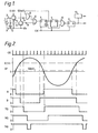
- FIG. 1 shows a circuit diagram of a processor and Figure 2 shows waveforms occurring in various parts of the circuit.
- the processor is connected to a tachogenerator 1 via terminals 2 and 3.
- Terminal 2 is connected to the voltage sensing input of a first voltage level comparator 4 and a second voltage level comparator 5.
- the output A of comparator 4 is connected to one input of an OR-gate 6 the output of which is connected to the D input of a delay-type flip-flop 7.
- the output B of comparator 5 is connected to one input of an AND-gate 8 the other input of which is connected to the Q output of flip-flop 7, which Q output is also connected to the D input of a further delay-type flip-flop 9.
- the output of AND-gate 8 is connected to the other input of gate 8.
- the Q output of flip-flop 9 is connected to one input of NAND-gate 10 the other input of which is connected to the Q output of flip-flop 7.
- the output of gate 10 is connected to the D input of a third delay-type flip-flop 11 whose Q output constitutes the processor output.
- Flip-flops 7, 9, and 11 are each fed with clock pulses CK having a pulse repetition rate, for example 80 kHz, considerably greater than the highest frequency output of tachogenerator 1 under working conditions.
- waveform OP is the output voltage waveform of tachogenerator 9 and the 50 mV and 0.5 V comparator levels are also shown.
- the remaining waveforms have logic 1 or 0 values and are designated in a corresponding manner to the circuit point concerned; that is to say that, for example, the waveform at the Q output of flip-flop 7 is designated 7Q in the drawing and in the following description.
- the change of state of the delay flip-flops 7, 9, and 11 is effected by the next subsequent clock pulse to the instant of the last change of state of the D input. Further, the repetition frequency of the clock pulses is too high in relation to the frequency of waveform OP to be shown on the same time scale. These clock pulses are therefore shown with a very considerably reduced frequency so that the sequence of operations may be clear.
- comparator 5 When the voltage OP rises to +0.5 mV, comparator 5 provides a B ⁇ 0 output. This causes 7D ⁇ 0 and, at the next clock pulse, 7Q ⁇ 0.
- One further clock pulse later flip-flop 11 responds to the 0 output of gate 10 one pulse earlier and 11Q ⁇ 0 to provide the leading edge of a processor output pulse. This same further clock pulse causes 9Q ⁇ 0, in response to which 11Q ⁇ 1 one clock pulse later.
- an output pulse is generated having a width of 12i microseconds assuming an 80 kHz clock rate.
- this voltage is between substantially zero (+50 mV) and three quarters of the negative peak voltage generated by the tachogenerator when running at its minimum speed (and hence minimum voltage) in the predetermined speed range over which the tachogenerator is used in practice.
- the peak output voltage is 0.75 volt and the most negative voltage level for comparator 4 would thus be approximately 0.56 volt.
- the reference voltage should be sufficiently less than the a.c. minimum peak value to ensure that signal A sets the latch to 1 safely, that is to say that the a.c. voltage exceeds the reference level for a greater time than the duration of at least most noise pulses which might otherwise mask it.
- the minimum reference level for comparator 4 should be high enough to give good noise immunity but must not be so close to the minimum peak voltage that it can be masked by noise. Accordingly a range of one third to three quarters of the peak value is suitable, the optimum being about two thirds of the peak value in each case.
- the output pulse is provided in the positive-going half cycles.
- the negative half cycles could, of course, equally well be used.
Landscapes
- Physics & Mathematics (AREA)
- General Physics & Mathematics (AREA)
- Nonlinear Science (AREA)
- Manipulation Of Pulses (AREA)
- Measurement Of Current Or Voltage (AREA)
Applications Claiming Priority (2)
| Application Number | Priority Date | Filing Date | Title |
|---|---|---|---|
| GB8123481 | 1981-07-31 | ||
| GB08123481A GB2105469A (en) | 1981-07-31 | 1981-07-31 | Tachogenerator output signal processor |
Publications (2)
| Publication Number | Publication Date |
|---|---|
| EP0071310A2 true EP0071310A2 (de) | 1983-02-09 |
| EP0071310A3 EP0071310A3 (de) | 1984-05-23 |
Family
ID=10523600
Family Applications (1)
| Application Number | Title | Priority Date | Filing Date |
|---|---|---|---|
| EP82200935A Withdrawn EP0071310A3 (de) | 1981-07-31 | 1982-07-22 | Verarbeitungsanlage für Ausgangssignale eines Tachogenerators |
Country Status (2)
| Country | Link |
|---|---|
| EP (1) | EP0071310A3 (de) |
| GB (1) | GB2105469A (de) |
Families Citing this family (1)
| Publication number | Priority date | Publication date | Assignee | Title |
|---|---|---|---|---|
| US10250241B2 (en) * | 2015-01-15 | 2019-04-02 | Infineon Technologies Ag | Asynchronous output protocol |
Family Cites Families (7)
| Publication number | Priority date | Publication date | Assignee | Title |
|---|---|---|---|---|
| US3582665A (en) * | 1968-08-16 | 1971-06-01 | Us Navy | Latching threshold detector |
| US3593166A (en) * | 1969-12-17 | 1971-07-13 | Bell Telephone Labor Inc | Zero crossing detector |
| US3639779A (en) * | 1971-03-15 | 1972-02-01 | Gte Sylvania Inc | Limiter circuit with enable function |
| US3727079A (en) * | 1971-12-06 | 1973-04-10 | Ampex | Zero crossing detecting circuit |
| US3955102A (en) * | 1973-11-21 | 1976-05-04 | Digital Equipment Corporation | Zero crossing detecting circuit |
| US3950705A (en) * | 1974-12-23 | 1976-04-13 | Tull Aviation Corporation | Noise rejection method and apparatus for digital data systems |
| ZA805412B (en) * | 1979-09-14 | 1981-08-26 | Plessey Overseas | Zero-crossing comparators with threshold validation |
-
1981
- 1981-07-31 GB GB08123481A patent/GB2105469A/en not_active Withdrawn
-
1982
- 1982-07-22 EP EP82200935A patent/EP0071310A3/de not_active Withdrawn
Also Published As
| Publication number | Publication date |
|---|---|
| GB2105469A (en) | 1983-03-23 |
| EP0071310A3 (de) | 1984-05-23 |
Similar Documents
| Publication | Publication Date | Title |
|---|---|---|
| US5294877A (en) | Circuit and method for detecting deceleration rates of a polyphase DC motor | |
| EP0487743B1 (de) | Mikrorechner mit eingebautem d/a-wandler | |
| US4800295A (en) | Retriggerable monostable multivibrator | |
| US4717864A (en) | Speed control method and apparatus for electronically commutated motors | |
| US4636656A (en) | Circuit for selectively extending a cycle of a clock signal | |
| WO1992012501A1 (en) | Apparatus and method for improving the resolution with which a test signal is counted | |
| US4962470A (en) | Crankshaft pulse position developing apparatus having a synchronous digital filter | |
| CA1154165A (en) | Manchester decoder | |
| US4282489A (en) | Metastable detector | |
| US4446389A (en) | Quadrature tach decoder circuit | |
| US3949394A (en) | Read amplifier having retriggerable, variable duty cycle inhibit pulse generator | |
| EP0071310A2 (de) | Verarbeitungsanlage für Ausgangssignale eines Tachogenerators | |
| US4425514A (en) | Fixed pulse width, fast recovery one-shot pulse generator | |
| JPS63268312A (ja) | 電流サージ制御集積回路 | |
| CA1143479A (en) | Noise eliminator circuit | |
| US4669098A (en) | Increased resolution counting circuit | |
| US3935475A (en) | Two-phase MOS synchronizer | |
| US5414307A (en) | Power reset circuit | |
| US5001364A (en) | Threshold crossing detector | |
| US4308502A (en) | Threshold detection | |
| US5506533A (en) | Apparatus for generating a monostable signal | |
| US4558457A (en) | Counter circuit having improved output response | |
| JPS6212521B2 (de) | ||
| US4164712A (en) | Continuous counting system | |
| JPS6348456B2 (de) |
Legal Events
| Date | Code | Title | Description |
|---|---|---|---|
| PUAI | Public reference made under article 153(3) epc to a published international application that has entered the european phase |
Free format text: ORIGINAL CODE: 0009012 |
|
| 17P | Request for examination filed |
Effective date: 19820722 |
|
| AK | Designated contracting states |
Designated state(s): DE FR GB IT |
|
| PUAL | Search report despatched |
Free format text: ORIGINAL CODE: 0009013 |
|
| AK | Designated contracting states |
Designated state(s): DE FR GB IT |
|
| STAA | Information on the status of an ep patent application or granted ep patent |
Free format text: STATUS: THE APPLICATION IS DEEMED TO BE WITHDRAWN |
|
| 18D | Application deemed to be withdrawn |
Effective date: 19850322 |
|
| RIN1 | Information on inventor provided before grant (corrected) |
Inventor name: SETH, SIYA VALLABH Inventor name: KEULEMANS, ALEXANDER HENDRIK FRANCIS |