EP0072938A2 - Procédé pour connecter une puce semi-conductrice à un support de puce - Google Patents
Procédé pour connecter une puce semi-conductrice à un support de puce Download PDFInfo
- Publication number
- EP0072938A2 EP0072938A2 EP82106929A EP82106929A EP0072938A2 EP 0072938 A2 EP0072938 A2 EP 0072938A2 EP 82106929 A EP82106929 A EP 82106929A EP 82106929 A EP82106929 A EP 82106929A EP 0072938 A2 EP0072938 A2 EP 0072938A2
- Authority
- EP
- European Patent Office
- Prior art keywords
- chip
- semiconductor
- semiconductor chip
- laser
- laser beam
- Prior art date
- Legal status (The legal status is an assumption and is not a legal conclusion. Google has not performed a legal analysis and makes no representation as to the accuracy of the status listed.)
- Granted
Links
Images
Classifications
-
- H—ELECTRICITY
- H10—SEMICONDUCTOR DEVICES; ELECTRIC SOLID-STATE DEVICES NOT OTHERWISE PROVIDED FOR
- H10P—GENERIC PROCESSES OR APPARATUS FOR THE MANUFACTURE OR TREATMENT OF DEVICES COVERED BY CLASS H10
- H10P34/00—Irradiation with electromagnetic or particle radiation of wafers, substrates or parts of devices
- H10P34/40—Irradiation with electromagnetic or particle radiation of wafers, substrates or parts of devices with high-energy radiation
- H10P34/42—Irradiation with electromagnetic or particle radiation of wafers, substrates or parts of devices with high-energy radiation with electromagnetic radiation, e.g. laser annealing
-
- H—ELECTRICITY
- H10—SEMICONDUCTOR DEVICES; ELECTRIC SOLID-STATE DEVICES NOT OTHERWISE PROVIDED FOR
- H10W—GENERIC PACKAGES, INTERCONNECTIONS, CONNECTORS OR OTHER CONSTRUCTIONAL DETAILS OF DEVICES COVERED BY CLASS H10
- H10W72/00—Interconnections or connectors in packages
- H10W72/30—Die-attach connectors
-
- H—ELECTRICITY
- H10—SEMICONDUCTOR DEVICES; ELECTRIC SOLID-STATE DEVICES NOT OTHERWISE PROVIDED FOR
- H10W—GENERIC PACKAGES, INTERCONNECTIONS, CONNECTORS OR OTHER CONSTRUCTIONAL DETAILS OF DEVICES COVERED BY CLASS H10
- H10W72/00—Interconnections or connectors in packages
- H10W72/071—Connecting or disconnecting
- H10W72/073—Connecting or disconnecting of die-attach connectors
- H10W72/07331—Connecting techniques
- H10W72/07336—Soldering or alloying
-
- H—ELECTRICITY
- H10—SEMICONDUCTOR DEVICES; ELECTRIC SOLID-STATE DEVICES NOT OTHERWISE PROVIDED FOR
- H10W—GENERIC PACKAGES, INTERCONNECTIONS, CONNECTORS OR OTHER CONSTRUCTIONAL DETAILS OF DEVICES COVERED BY CLASS H10
- H10W72/00—Interconnections or connectors in packages
- H10W72/071—Connecting or disconnecting
- H10W72/073—Connecting or disconnecting of die-attach connectors
- H10W72/07331—Connecting techniques
- H10W72/07337—Connecting techniques using a polymer adhesive, e.g. an adhesive based on silicone or epoxy
-
- H—ELECTRICITY
- H10—SEMICONDUCTOR DEVICES; ELECTRIC SOLID-STATE DEVICES NOT OTHERWISE PROVIDED FOR
- H10W—GENERIC PACKAGES, INTERCONNECTIONS, CONNECTORS OR OTHER CONSTRUCTIONAL DETAILS OF DEVICES COVERED BY CLASS H10
- H10W72/00—Interconnections or connectors in packages
- H10W72/30—Die-attach connectors
- H10W72/351—Materials of die-attach connectors
- H10W72/352—Materials of die-attach connectors comprising metals or metalloids, e.g. solders
-
- Y—GENERAL TAGGING OF NEW TECHNOLOGICAL DEVELOPMENTS; GENERAL TAGGING OF CROSS-SECTIONAL TECHNOLOGIES SPANNING OVER SEVERAL SECTIONS OF THE IPC; TECHNICAL SUBJECTS COVERED BY FORMER USPC CROSS-REFERENCE ART COLLECTIONS [XRACs] AND DIGESTS
- Y10—TECHNICAL SUBJECTS COVERED BY FORMER USPC
- Y10T—TECHNICAL SUBJECTS COVERED BY FORMER US CLASSIFICATION
- Y10T156/00—Adhesive bonding and miscellaneous chemical manufacture
- Y10T156/10—Methods of surface bonding and/or assembly therefor
- Y10T156/1002—Methods of surface bonding and/or assembly therefor with permanent bending or reshaping or surface deformation of self sustaining lamina
Definitions
- the invention relates to a method for connecting a semiconductor chip to a chip carrier by gluing or soldering.
- Semiconductor chips such as. B. integrated semiconductor circuits or power devices are soldered or glued on one side to metal carrier plates or metallized ceramic carrier plates.
- the soldering or gluing point must be mechanically so permanent that it is not destroyed by frequent load changes and the associated shear stresses between the semiconductor chip and the chip carrier. Since the chip carrier also serves either as a heat sink itself or else has to dissipate the heat to a heat sink, the lowest possible, reproducible thermal contact resistance between the semiconductor chip and the chip carrier should also be sought.
- the invention has for its object to provide a method of the type specified above, with which an optimal durability of the connection point can be achieved with a low and reproducible thermal contact resistance.
- the invention is characterized in that the surface of the semiconductor chip to be connected is treated by means of a laser beam and in that the energy of the laser beam is adjusted in such a way that by local exposure melting of the semiconductor material depressions are generated and the molten semiconductor material is at least partially thrown up at the edge of the depression.
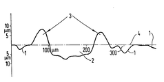
- the resulting cross section through such a crater is shown in the figure.
- the contour of the retained silicon surface is designated by 1.
- the resulting crater bears the reference number 2, while 3 on the edge of the depression is drawing.
- the depth of the depression and the height of the throw-up are measured from an imaginary line 4, which is placed over the maxima of the original silicon surface.
- the width or the diameter of the recess should be measured at the level of the imaginary plane.
- the ratio of the area of all depressions 2 to the area of the semiconductor chip not treated by laser should be at least 30%.
- a good clawing of the solder or the adhesive to the surface of the semiconductor chip and a good connection between the semiconductor chip and the chip carrier are thus achieved.
- the throw 3 ensures a defined distance between the semiconductor chip and the chip carrier, so that the thermal contact resistance can be reproduced exactly.
- the remaining cavities between the semiconductor chip and the chip carrier are then filled with the conductive adhesive or with the solder.
- the entire surface of the semiconductor chip to be connected is expediently metallized before the soldering or gluing. This can reduce the thermal contact resistance and improve the electrical contact.
Landscapes
- Die Bonding (AREA)
- Laser Beam Processing (AREA)
Applications Claiming Priority (2)
| Application Number | Priority Date | Filing Date | Title |
|---|---|---|---|
| DE3132983 | 1981-08-20 | ||
| DE19813132983 DE3132983A1 (de) | 1981-08-20 | 1981-08-20 | Verfahren zum verbinden eines halbleiterchips mit einem chiptraeger |
Publications (3)
| Publication Number | Publication Date |
|---|---|
| EP0072938A2 true EP0072938A2 (fr) | 1983-03-02 |
| EP0072938A3 EP0072938A3 (en) | 1985-01-09 |
| EP0072938B1 EP0072938B1 (fr) | 1986-12-03 |
Family
ID=6139751
Family Applications (1)
| Application Number | Title | Priority Date | Filing Date |
|---|---|---|---|
| EP82106929A Expired EP0072938B1 (fr) | 1981-08-20 | 1982-07-30 | Procédé pour connecter une puce semi-conductrice à un support de puce |
Country Status (4)
| Country | Link |
|---|---|
| US (1) | US4746390A (fr) |
| EP (1) | EP0072938B1 (fr) |
| JP (1) | JPS5842244A (fr) |
| DE (2) | DE3132983A1 (fr) |
Families Citing this family (11)
| Publication number | Priority date | Publication date | Assignee | Title |
|---|---|---|---|---|
| US4861407A (en) * | 1985-06-18 | 1989-08-29 | The Dow Chemical Company | Method for adhesive bonding articles via pretreatment with energy beams |
| US4968383A (en) * | 1985-06-18 | 1990-11-06 | The Dow Chemical Company | Method for molding over a preform |
| DE3725269A1 (de) * | 1987-07-30 | 1989-02-09 | Messerschmitt Boelkow Blohm | Verfahren zum einkapseln von mikroelektronischen halbleiter- und schichtschaltungen |
| US5314003A (en) * | 1991-12-24 | 1994-05-24 | Microelectronics And Computer Technology Corporation | Three-dimensional metal fabrication using a laser |
| DE4235908A1 (de) * | 1992-10-23 | 1994-04-28 | Telefunken Microelectron | Verfahren zum Verlöten eines Halbleiterkörpers mit einem Trägerelement |
| AU5416694A (en) * | 1992-10-28 | 1994-05-24 | Jorg Meyer | Metal-plastic composite, process for producing it and apparatus for carrying out the process |
| US20020170897A1 (en) * | 2001-05-21 | 2002-11-21 | Hall Frank L. | Methods for preparing ball grid array substrates via use of a laser |
| JP5077536B2 (ja) * | 2007-05-08 | 2012-11-21 | 富士電機株式会社 | 半導体装置の製造方法 |
| US8802553B2 (en) | 2011-02-10 | 2014-08-12 | Infineon Technologies Ag | Method for mounting a semiconductor chip on a carrier |
| JP6441295B2 (ja) * | 2016-12-26 | 2018-12-19 | 本田技研工業株式会社 | 接合構造体及びその製造方法 |
| EP4292479A1 (fr) | 2020-06-19 | 2023-12-20 | The Ergo Baby Carrier, Inc. | Porte-bébé réglable à orientations de transport multiples |
Family Cites Families (12)
| Publication number | Priority date | Publication date | Assignee | Title |
|---|---|---|---|---|
| DE875968C (de) * | 1951-09-04 | 1953-05-07 | Licentia Gmbh | Elektrisch unsymmetrisch leitendes System |
| DE1414425A1 (de) * | 1959-06-11 | 1968-10-10 | Siemens Ag | Verfahren zum Einlegieren von Elektrodenmaterial in einen Halbleiterkoerper |
| US3945111A (en) * | 1974-01-03 | 1976-03-23 | Motorola, Inc. | Metallization system for semiconductor devices, devices utilizing such metallization system and method for making devices and metallization system |
| DE2458370C2 (de) * | 1974-12-10 | 1984-05-10 | Dr.-Ing. Rudolf Hell Gmbh, 2300 Kiel | Energiestrahl-Gravierverfahren und Einrichtung zu seiner Durchführung |
| US4050507A (en) * | 1975-06-27 | 1977-09-27 | International Business Machines Corporation | Method for customizing nucleate boiling heat transfer from electronic units immersed in dielectric coolant |
| JPS5946415B2 (ja) * | 1978-04-28 | 1984-11-12 | 株式会社日立製作所 | 半導体装置の製造方法 |
| US4200382A (en) * | 1978-08-30 | 1980-04-29 | Polaroid Corporation | Photographic processing roller and a novel method which utilizes a pulsed laser for manufacturing the roller |
| JPS5837713B2 (ja) * | 1978-12-01 | 1983-08-18 | 富士通株式会社 | 半導体レ−ザ−装置の製造方法 |
| IT1119679B (it) * | 1979-03-05 | 1986-03-10 | Fiat Auto Spa | Apparecchiatura per effettuare trattamenti su pezzi metallici mediante |
| JPS55175242U (fr) * | 1979-06-04 | 1980-12-16 | ||
| US4257827A (en) * | 1979-11-13 | 1981-03-24 | International Business Machines Corporation | High efficiency gettering in silicon through localized superheated melt formation |
| US4359486A (en) * | 1980-08-28 | 1982-11-16 | Siemens Aktiengesellschaft | Method of producing alloyed metal contact layers on crystal-orientated semiconductor surfaces by energy pulse irradiation |
-
1981
- 1981-08-20 DE DE19813132983 patent/DE3132983A1/de not_active Withdrawn
-
1982
- 1982-07-29 US US06/402,847 patent/US4746390A/en not_active Expired - Fee Related
- 1982-07-30 DE DE8282106929T patent/DE3274600D1/de not_active Expired
- 1982-07-30 EP EP82106929A patent/EP0072938B1/fr not_active Expired
- 1982-08-17 JP JP57142568A patent/JPS5842244A/ja active Granted
Also Published As
| Publication number | Publication date |
|---|---|
| EP0072938B1 (fr) | 1986-12-03 |
| EP0072938A3 (en) | 1985-01-09 |
| DE3132983A1 (de) | 1983-03-03 |
| JPH0230576B2 (fr) | 1990-07-06 |
| DE3274600D1 (en) | 1987-01-15 |
| US4746390A (en) | 1988-05-24 |
| JPS5842244A (ja) | 1983-03-11 |
Similar Documents
| Publication | Publication Date | Title |
|---|---|---|
| DE3209242C2 (de) | Verfahren zum Anbringen von Kontakterhöhungen an Kontaktstellen einer elektronischen Mikroschaltung | |
| DE10229182B4 (de) | Verfahren zur Herstellung einer gestapelten Chip-Packung | |
| EP0283590A2 (fr) | Composants électriques | |
| EP0072938B1 (fr) | Procédé pour connecter une puce semi-conductrice à un support de puce | |
| DE3616494A1 (de) | Integrierte schaltungspackung und verfahren zur herstellung einer integrierten schaltungspackung | |
| DE4010370C2 (de) | Verfahren zum Herstellen von Halbleiterbauteilen | |
| EP0351581A1 (fr) | Circuit intégré à haute densité et procédé pour sa fabrication | |
| DE112019005844T5 (de) | Halbleiterbauteil | |
| EP0140126A1 (fr) | Procédé de montage automatique sur bande | |
| DE3824008A1 (de) | Elektronische schaltung sowie verfahren zu deren herstellung | |
| DE102010038933A1 (de) | Halbleitervorrichtung mit Halbleiterchip und Metallplatte und Verfahren zu deren Fertigung | |
| EP0152818A2 (fr) | Module semi-conducteur de puissance | |
| EP1680949B1 (fr) | Procédé de fabrication d'une barrière d'arrêt de brasure | |
| DE2730566C3 (de) | Halbleitervorrichtung mit einem pn-übergang und Verfahren zu ihrer Herstellung | |
| DE2656019C3 (de) | Vorrichtung zum Ausrichten und Anlöten von Podesten bzw. Ronden bezüglich der bzw. an den lötfähigen ohmschen Kontakten) von Halbleiterbauelementen | |
| DE112019004482T5 (de) | Bond-Struktur, Halbleiterbauteil und Verfahren zum Bilden einer Bond-Struktur | |
| DE19707887C2 (de) | Verfahren zum Herstellen und Trennen von elektronischen Elementen mit leitfähigen Kontaktanschlüssen | |
| DE112019004313T5 (de) | Gehäusestruktur, halbleiterbauteil und verfahren zum bilden einer gehäusestruktur | |
| DE102022101523A1 (de) | Halbleitervorrichtung und Verfahren zum Herstellen derselben | |
| EP0303272A2 (fr) | Circuit imprimé pour l'électronique | |
| DE2332822A1 (de) | Verfahren zum herstellen von diffundierten, kontaktierten und oberflaechenpassivierten halbleiterscheiben fuer halbleiterbauelement | |
| DE2528000A1 (de) | Verfahren zur herstellung einer loetflaeche relativ grosser abmessungen | |
| EP0104580B1 (fr) | Procédé de fabrication de composants électriques en forme de pastille | |
| DE10341186A1 (de) | Verfahren und Vorrichtung zum Kontaktieren von Halbleiterchips | |
| DE19738118C2 (de) | Montageverfahren für ein Halbleiterbauelement |
Legal Events
| Date | Code | Title | Description |
|---|---|---|---|
| PUAI | Public reference made under article 153(3) epc to a published international application that has entered the european phase |
Free format text: ORIGINAL CODE: 0009012 |
|
| AK | Designated contracting states |
Designated state(s): CH DE FR GB IT LI |
|
| PUAL | Search report despatched |
Free format text: ORIGINAL CODE: 0009013 |
|
| AK | Designated contracting states |
Designated state(s): CH DE FR GB IT LI |
|
| 17P | Request for examination filed |
Effective date: 19841214 |
|
| 17Q | First examination report despatched |
Effective date: 19860121 |
|
| GRAA | (expected) grant |
Free format text: ORIGINAL CODE: 0009210 |
|
| AK | Designated contracting states |
Kind code of ref document: B1 Designated state(s): CH DE FR GB IT LI |
|
| REF | Corresponds to: |
Ref document number: 3274600 Country of ref document: DE Date of ref document: 19870115 |
|
| ET | Fr: translation filed | ||
| ITF | It: translation for a ep patent filed | ||
| PLBE | No opposition filed within time limit |
Free format text: ORIGINAL CODE: 0009261 |
|
| STAA | Information on the status of an ep patent application or granted ep patent |
Free format text: STATUS: NO OPPOSITION FILED WITHIN TIME LIMIT |
|
| 26N | No opposition filed | ||
| PG25 | Lapsed in a contracting state [announced via postgrant information from national office to epo] |
Ref country code: GB Effective date: 19880730 |
|
| PG25 | Lapsed in a contracting state [announced via postgrant information from national office to epo] |
Ref country code: LI Effective date: 19880731 Ref country code: CH Effective date: 19880731 |
|
| GBPC | Gb: european patent ceased through non-payment of renewal fee | ||
| PG25 | Lapsed in a contracting state [announced via postgrant information from national office to epo] |
Ref country code: FR Free format text: LAPSE BECAUSE OF NON-PAYMENT OF DUE FEES Effective date: 19890331 |
|
| REG | Reference to a national code |
Ref country code: CH Ref legal event code: PL |
|
| REG | Reference to a national code |
Ref country code: FR Ref legal event code: ST |
|
| PG25 | Lapsed in a contracting state [announced via postgrant information from national office to epo] |
Ref country code: DE Effective date: 19900403 |