EP0073172A2 - Technique pour connexion de fils pour puces à circuit intégré - Google Patents
Technique pour connexion de fils pour puces à circuit intégré Download PDFInfo
- Publication number
- EP0073172A2 EP0073172A2 EP82401558A EP82401558A EP0073172A2 EP 0073172 A2 EP0073172 A2 EP 0073172A2 EP 82401558 A EP82401558 A EP 82401558A EP 82401558 A EP82401558 A EP 82401558A EP 0073172 A2 EP0073172 A2 EP 0073172A2
- Authority
- EP
- European Patent Office
- Prior art keywords
- lead frame
- frame finger
- bonding
- finger
- lead
- Prior art date
- Legal status (The legal status is an assumption and is not a legal conclusion. Google has not performed a legal analysis and makes no representation as to the accuracy of the status listed.)
- Withdrawn
Links
Images




Classifications
-
- H—ELECTRICITY
- H10—SEMICONDUCTOR DEVICES; ELECTRIC SOLID-STATE DEVICES NOT OTHERWISE PROVIDED FOR
- H10W—GENERIC PACKAGES, INTERCONNECTIONS, CONNECTORS OR OTHER CONSTRUCTIONAL DETAILS OF DEVICES COVERED BY CLASS H10
- H10W70/00—Package substrates; Interposers; Redistribution layers [RDL]
- H10W70/01—Manufacture or treatment
- H10W70/04—Manufacture or treatment of leadframes
- H10W70/041—Connecting or disconnecting interconnections to or from leadframes, e.g. connecting bond wires or bumps
-
- H—ELECTRICITY
- H10—SEMICONDUCTOR DEVICES; ELECTRIC SOLID-STATE DEVICES NOT OTHERWISE PROVIDED FOR
- H10W—GENERIC PACKAGES, INTERCONNECTIONS, CONNECTORS OR OTHER CONSTRUCTIONAL DETAILS OF DEVICES COVERED BY CLASS H10
- H10W72/00—Interconnections or connectors in packages
- H10W72/071—Connecting or disconnecting
-
- H—ELECTRICITY
- H10—SEMICONDUCTOR DEVICES; ELECTRIC SOLID-STATE DEVICES NOT OTHERWISE PROVIDED FOR
- H10W—GENERIC PACKAGES, INTERCONNECTIONS, CONNECTORS OR OTHER CONSTRUCTIONAL DETAILS OF DEVICES COVERED BY CLASS H10
- H10W72/00—Interconnections or connectors in packages
- H10W72/01—Manufacture or treatment
- H10W72/0198—Manufacture or treatment batch processes
-
- H—ELECTRICITY
- H10—SEMICONDUCTOR DEVICES; ELECTRIC SOLID-STATE DEVICES NOT OTHERWISE PROVIDED FOR
- H10W—GENERIC PACKAGES, INTERCONNECTIONS, CONNECTORS OR OTHER CONSTRUCTIONAL DETAILS OF DEVICES COVERED BY CLASS H10
- H10W72/00—Interconnections or connectors in packages
- H10W72/071—Connecting or disconnecting
- H10W72/0711—Apparatus therefor
- H10W72/07141—Means for applying energy, e.g. ovens or lasers
-
- H—ELECTRICITY
- H10—SEMICONDUCTOR DEVICES; ELECTRIC SOLID-STATE DEVICES NOT OTHERWISE PROVIDED FOR
- H10W—GENERIC PACKAGES, INTERCONNECTIONS, CONNECTORS OR OTHER CONSTRUCTIONAL DETAILS OF DEVICES COVERED BY CLASS H10
- H10W72/00—Interconnections or connectors in packages
- H10W72/071—Connecting or disconnecting
- H10W72/075—Connecting or disconnecting of bond wires
-
- H—ELECTRICITY
- H10—SEMICONDUCTOR DEVICES; ELECTRIC SOLID-STATE DEVICES NOT OTHERWISE PROVIDED FOR
- H10W—GENERIC PACKAGES, INTERCONNECTIONS, CONNECTORS OR OTHER CONSTRUCTIONAL DETAILS OF DEVICES COVERED BY CLASS H10
- H10W72/00—Interconnections or connectors in packages
- H10W72/071—Connecting or disconnecting
- H10W72/075—Connecting or disconnecting of bond wires
- H10W72/07511—Treating the bonding area before connecting, e.g. by applying flux or cleaning
-
- H—ELECTRICITY
- H10—SEMICONDUCTOR DEVICES; ELECTRIC SOLID-STATE DEVICES NOT OTHERWISE PROVIDED FOR
- H10W—GENERIC PACKAGES, INTERCONNECTIONS, CONNECTORS OR OTHER CONSTRUCTIONAL DETAILS OF DEVICES COVERED BY CLASS H10
- H10W72/00—Interconnections or connectors in packages
- H10W72/071—Connecting or disconnecting
- H10W72/075—Connecting or disconnecting of bond wires
- H10W72/07521—Aligning
-
- H—ELECTRICITY
- H10—SEMICONDUCTOR DEVICES; ELECTRIC SOLID-STATE DEVICES NOT OTHERWISE PROVIDED FOR
- H10W—GENERIC PACKAGES, INTERCONNECTIONS, CONNECTORS OR OTHER CONSTRUCTIONAL DETAILS OF DEVICES COVERED BY CLASS H10
- H10W72/00—Interconnections or connectors in packages
- H10W72/071—Connecting or disconnecting
- H10W72/075—Connecting or disconnecting of bond wires
- H10W72/07531—Techniques
- H10W72/07532—Compression bonding, e.g. thermocompression bonding
-
- H—ELECTRICITY
- H10—SEMICONDUCTOR DEVICES; ELECTRIC SOLID-STATE DEVICES NOT OTHERWISE PROVIDED FOR
- H10W—GENERIC PACKAGES, INTERCONNECTIONS, CONNECTORS OR OTHER CONSTRUCTIONAL DETAILS OF DEVICES COVERED BY CLASS H10
- H10W72/00—Interconnections or connectors in packages
- H10W72/071—Connecting or disconnecting
- H10W72/075—Connecting or disconnecting of bond wires
- H10W72/07531—Techniques
- H10W72/07532—Compression bonding, e.g. thermocompression bonding
- H10W72/07533—Ultrasonic bonding, e.g. thermosonic bonding
-
- H—ELECTRICITY
- H10—SEMICONDUCTOR DEVICES; ELECTRIC SOLID-STATE DEVICES NOT OTHERWISE PROVIDED FOR
- H10W—GENERIC PACKAGES, INTERCONNECTIONS, CONNECTORS OR OTHER CONSTRUCTIONAL DETAILS OF DEVICES COVERED BY CLASS H10
- H10W72/00—Interconnections or connectors in packages
- H10W72/071—Connecting or disconnecting
- H10W72/075—Connecting or disconnecting of bond wires
- H10W72/07541—Controlling the environment, e.g. atmosphere composition or temperature
-
- H—ELECTRICITY
- H10—SEMICONDUCTOR DEVICES; ELECTRIC SOLID-STATE DEVICES NOT OTHERWISE PROVIDED FOR
- H10W—GENERIC PACKAGES, INTERCONNECTIONS, CONNECTORS OR OTHER CONSTRUCTIONAL DETAILS OF DEVICES COVERED BY CLASS H10
- H10W72/00—Interconnections or connectors in packages
- H10W72/50—Bond wires
- H10W72/531—Shapes of wire connectors
- H10W72/533—Cross-sectional shape
- H10W72/534—Cross-sectional shape being rectangular
-
- H—ELECTRICITY
- H10—SEMICONDUCTOR DEVICES; ELECTRIC SOLID-STATE DEVICES NOT OTHERWISE PROVIDED FOR
- H10W—GENERIC PACKAGES, INTERCONNECTIONS, CONNECTORS OR OTHER CONSTRUCTIONAL DETAILS OF DEVICES COVERED BY CLASS H10
- H10W72/00—Interconnections or connectors in packages
- H10W72/50—Bond wires
- H10W72/531—Shapes of wire connectors
- H10W72/536—Shapes of wire connectors the connected ends being ball-shaped
-
- H—ELECTRICITY
- H10—SEMICONDUCTOR DEVICES; ELECTRIC SOLID-STATE DEVICES NOT OTHERWISE PROVIDED FOR
- H10W—GENERIC PACKAGES, INTERCONNECTIONS, CONNECTORS OR OTHER CONSTRUCTIONAL DETAILS OF DEVICES COVERED BY CLASS H10
- H10W72/00—Interconnections or connectors in packages
- H10W72/50—Bond wires
- H10W72/531—Shapes of wire connectors
- H10W72/5363—Shapes of wire connectors the connected ends being wedge-shaped
-
- H—ELECTRICITY
- H10—SEMICONDUCTOR DEVICES; ELECTRIC SOLID-STATE DEVICES NOT OTHERWISE PROVIDED FOR
- H10W—GENERIC PACKAGES, INTERCONNECTIONS, CONNECTORS OR OTHER CONSTRUCTIONAL DETAILS OF DEVICES COVERED BY CLASS H10
- H10W72/00—Interconnections or connectors in packages
- H10W72/50—Bond wires
- H10W72/551—Materials of bond wires
- H10W72/552—Materials of bond wires comprising metals or metalloids, e.g. silver
-
- H—ELECTRICITY
- H10—SEMICONDUCTOR DEVICES; ELECTRIC SOLID-STATE DEVICES NOT OTHERWISE PROVIDED FOR
- H10W—GENERIC PACKAGES, INTERCONNECTIONS, CONNECTORS OR OTHER CONSTRUCTIONAL DETAILS OF DEVICES COVERED BY CLASS H10
- H10W72/00—Interconnections or connectors in packages
- H10W72/50—Bond wires
- H10W72/551—Materials of bond wires
- H10W72/552—Materials of bond wires comprising metals or metalloids, e.g. silver
- H10W72/5522—Materials of bond wires comprising metals or metalloids, e.g. silver comprising gold [Au]
-
- H—ELECTRICITY
- H10—SEMICONDUCTOR DEVICES; ELECTRIC SOLID-STATE DEVICES NOT OTHERWISE PROVIDED FOR
- H10W—GENERIC PACKAGES, INTERCONNECTIONS, CONNECTORS OR OTHER CONSTRUCTIONAL DETAILS OF DEVICES COVERED BY CLASS H10
- H10W72/00—Interconnections or connectors in packages
- H10W72/50—Bond wires
- H10W72/551—Materials of bond wires
- H10W72/552—Materials of bond wires comprising metals or metalloids, e.g. silver
- H10W72/5524—Materials of bond wires comprising metals or metalloids, e.g. silver comprising aluminium [Al]
-
- H—ELECTRICITY
- H10—SEMICONDUCTOR DEVICES; ELECTRIC SOLID-STATE DEVICES NOT OTHERWISE PROVIDED FOR
- H10W—GENERIC PACKAGES, INTERCONNECTIONS, CONNECTORS OR OTHER CONSTRUCTIONAL DETAILS OF DEVICES COVERED BY CLASS H10
- H10W72/00—Interconnections or connectors in packages
- H10W72/50—Bond wires
- H10W72/551—Materials of bond wires
- H10W72/552—Materials of bond wires comprising metals or metalloids, e.g. silver
- H10W72/5525—Materials of bond wires comprising metals or metalloids, e.g. silver comprising copper [Cu]
-
- H—ELECTRICITY
- H10—SEMICONDUCTOR DEVICES; ELECTRIC SOLID-STATE DEVICES NOT OTHERWISE PROVIDED FOR
- H10W—GENERIC PACKAGES, INTERCONNECTIONS, CONNECTORS OR OTHER CONSTRUCTIONAL DETAILS OF DEVICES COVERED BY CLASS H10
- H10W72/00—Interconnections or connectors in packages
- H10W72/50—Bond wires
- H10W72/59—Bond pads specially adapted therefor
-
- H—ELECTRICITY
- H10—SEMICONDUCTOR DEVICES; ELECTRIC SOLID-STATE DEVICES NOT OTHERWISE PROVIDED FOR
- H10W—GENERIC PACKAGES, INTERCONNECTIONS, CONNECTORS OR OTHER CONSTRUCTIONAL DETAILS OF DEVICES COVERED BY CLASS H10
- H10W72/00—Interconnections or connectors in packages
- H10W72/90—Bond pads, in general
- H10W72/931—Shapes of bond pads
-
- H—ELECTRICITY
- H10—SEMICONDUCTOR DEVICES; ELECTRIC SOLID-STATE DEVICES NOT OTHERWISE PROVIDED FOR
- H10W—GENERIC PACKAGES, INTERCONNECTIONS, CONNECTORS OR OTHER CONSTRUCTIONAL DETAILS OF DEVICES COVERED BY CLASS H10
- H10W72/00—Interconnections or connectors in packages
- H10W72/90—Bond pads, in general
- H10W72/931—Shapes of bond pads
- H10W72/932—Plan-view shape, i.e. in top view
-
- H—ELECTRICITY
- H10—SEMICONDUCTOR DEVICES; ELECTRIC SOLID-STATE DEVICES NOT OTHERWISE PROVIDED FOR
- H10W—GENERIC PACKAGES, INTERCONNECTIONS, CONNECTORS OR OTHER CONSTRUCTIONAL DETAILS OF DEVICES COVERED BY CLASS H10
- H10W90/00—Package configurations
- H10W90/701—Package configurations characterised by the relative positions of pads or connectors relative to package parts
- H10W90/751—Package configurations characterised by the relative positions of pads or connectors relative to package parts of bond wires
- H10W90/756—Package configurations characterised by the relative positions of pads or connectors relative to package parts of bond wires between a chip and a stacked lead frame, conducting package substrate or heat sink
Definitions
- This invention relates to a new method and apparatus for welding or bonding a lead wire or bonding wire from an integrated circuit chip mounted on a lead frame to a lead frame finger or prong.
- the invention permits wire bonding to lead frames of common metals such as copper alloy, red brass and stainless steel without the need for gold or silver plating of the lead frame elements.
- lead wires of copper and other common metals may be used instead of gold and silver bonding wire.
- Integrated circuit or microcircuit chips are generally mounted on lead frames for coupling to external circuitry.
- Such lead frames are stamped in long strips or lengths of metal ribbon.
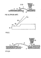
- a fragmentary portion of such a lead frame strip 6 showing two successive lead frames 5 is illustrated in Fig. 1.
- Each lead frame 5 includes a paddle 7 to which the microcircuit chip is secured by epoxy resin, and a plurality of lead frame fingers or prongs 8 which extend from a "dam" 9 toward the paddle to receive the lead wires from the chip.
- the ribbon is mounted on large reels for shipping to the customer.
- the lead frames are generally stamped from copper alloy, red brass, stainless steel, and similar metals. According to the conventional methods of lead wire bonding, the paddle and lead frame fingers must be plated with gold or silver in order to achieve good quality welds. In order to prepare the lead frames, the reels of stamped ribbon are shipped to another location for plating and stamping or cutting into shorter strips. The lead frames are thereafter shipped again to the microcircuit chip manufacturer for packaging the chips. Because of the extensive shipping and handling required the lead frame ribbons are frequently bent or damaged particularly during the shipping and handling of the large reels.
- Bonding of lead wires between a microcircuit chip and the lead frame on which the chip is mounted is generally accomplished by "ball/wedge" bonding.
- a lead wire or bonding wire 11 is held in a capillary tool 12 with the lead wire 11 projecting beyond the end of the tool as shown in Figure lA.
- the capillary tool 12 forms part of a bonding machine in which the tool is appropriately mounted and positioned over the metallized die pad 14 of an integrated circuit chip or substrate 17, mounted on paddle 7.
- a ball 15 of metal has been formed at the end of the lead wire or bonding wire 11 by melting for example with a hydrogen gas flame torch or by electric arc discharge.
- a bond is formed typically by thermocompression bonding applying a specified force and temperature for a specified period of time. Metallic welding and diffusion combine to form this basic bond. Alternatively, ultrasonic bonding or other form of welding may be used.
- the capillary tool 12 and substrate 17 are then moved relative to each other for bonding of the wire to lead frame finger 8.
- a wedge bond between the lead wire 11 and finger 8 is generally formed and the lead wire or bonding wire 11 is severed below the bonding tool at the weld.
- the wedge bond is formed by thermocompression or ultrasonic bonding with the edge of the capillary tool bearing against the wire and lead frame finger.
- a lead wire connection is established between the metallized substrate of a chip and the lead frame for coupling to external circuitry.
- the conventional approach to securing lead wire or bonding wire between the microcircuit chip and lead frame fingers is limited to methods in which the chip and lead frame finger are maintained at the same relatively low level temperature, a temperature below the level at which damage might occur to the chip.
- thermocompression and ultrasonic welding or bonding methods are used at temperatures typically no greater than for example 200°C.
- the ball bond must be formed first because it requires the use of the free end of the wire. Since this is the preferred bond at the chip, the ball bond to the chip is formed first.
- the capi- lla-ry tool then bears against the lead frame finger to effect the second bond.
- the lead frame finger is therefore electrically and thermally coupled to the chip during the second bond. Heating of the second bond by application of electrical energy is therefore severely limited because of the damage which might occur at the chip due to excessive voltage, current or temperature.
- gold or silver plating of the bonding surfaces i.e. the lead frame fingers
- gold or silver lead wire and bonding wire is also generally used for the same reasons.
- Copending United States Patent Application Serial No. 262,595 referred to above describes a new method and apparatus for ball bonding to the microcircuit chip using lead wires of copper, aluminum and other reactive metals in addition to gold and silver.
- the present invention carries this approach further to achieve high quality welds at the lead frame fingers for lead wires of copper etc. and furthermore without the need for gold or silver plating of the lead frame fingers.
- a feature and advantage of the elimination of gold or silver plating of the lead frame elements is that the extensive handling and shipping of the reels of lead frame ribbon is minimized thereby reducing the level of damage suffered by the ribbon as a result of such handling.
- Another object of the invention is to achieve bonding of lead wire between an integrated circuit chip and lead frame finger at differential temperatures, with the chip at a safe level temperature below the level at which damage might occur, while the lead frame finger is at temperatures significantly higher including the melting point temperature of the lead frame metal and temperatures at which damage might occur at the chip.
- a further object of the invention is to provide a welding method at the lead frame finger by which the primary energy for the weld is applied to the lead frame finger while it is isolated from electrical and thermal coupling with the chip.
- the invention also achieves intense but controlled application of energy for the weld without oxidation of the metal at the bond and while insuring the quality of the weld.
- one aspect of the invention involves a method for welding a lead wire or bonding wire to a metal lead frame finger where one end of the wire has already been bonded to a circuit chip on the lead frame preheating the lead frame finger to which the lead wire is to be bonded by application of electrical energy while the lead frame finger is isolated from electrical or thermal coupling with the circuit chip, such heating reaching a temperature above the safe level at which damage might occur to the circuit chip; bonding a section of the lead wire to the preheated lead frame finger; and severing the lead wire adjacent the bond at the lead frame finger.
- Another aspect of the invention is related to an apparatus for welding a lead wire or bonding wire to a metal lead frame finger where one end of the wire has already been bonded to a circuit chip on the lead frame, characterized by: means for preheating the lead frame finger to which the lead wire is to be bonded by application of electrical energy while the lead frame finger is isolated from electrical or thermal coupling with the circuit chip, such heating reaching a temperature above the safe level at which damage might occur to the circuit chip; means for bonding a section of the lead wire to the preheated lead frame finger; and means for severing the lead wire adjacent the bond at the lead frame finger.
- the specific implementation of invention contemplates preheating the lead frame finger by application of electrical energy prior to electrical or thermal contact of the capillary bonding tool or lead wire with the lead frame finger.
- the lead frame finger remains isolated from the chip during preheating of the lead frame finger to a second temperature level and by application of energy at a level above the safe level at which damage might occur to the microcircuit.
- lead wire may be bonded between the microcircuit chip and lead frame finger at differential temperatures and by application of differential welding energies. The lead wire is then bonded to the preheated or preenergized lead frame finger and after cooling is severed adjacent the bond.
- the lead frame finger is preheated to a temperature below the melting point of the metal comprising the lead frame. Bonding is thereafter effected by thermocompression or ultrasonic bonding with the capillary tool bearing against the lead frame finger only after the primary welding energy has been applied.
- the lead frame comprises red brass with a melting point in the range of 990°C to 1025°C
- the lead frame finger is preheated to a temperature in the range of approximately 500°C to 900°C, far above the safe level at which damage might occur to the chip.
- the preheating step comprises melting a portion of the surface of the lead frame finger thereby forming a molten pool or puddle in the surface prior to any electrcal or thermal coupling between the lead frame finger and microcircuit chip. Bonding of the lead wire to the lead frame finger is effected by immersing a section of the wire in the molten pool and allowing the pool to harden.
- the lead wire may be selected to have a melting point higher than the melting point of the lead frame metal. For example copper wire having a melting point of 1083°C may be used
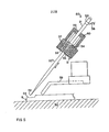
- bonding of lead wire from a microcircuit chip to the lead frame is effected by preheating each lead frame finger prior to electrical coupling or contact of the lead wire to the lead frame finger. This is generally accomplished by positioning a fine tipped electrode 20 over a lead frame finger 8 as shown in Fig. 2, for delivering a controlled amount of electrical energy to the bonding location. Electrical energy for preheating is delivered by discharging a controlled pulse train in an arc discharge between the electrode and lead frame finger all in an inert gas environment.
- a suitable electrode 20 is provided by a tungsten rod 21, for example 40 mils in diameter, melted and drawn to a point 22 one to several mils in diameter. The electrode is mounted for positioning sequentially over each lead frame finger, and for extension and retraction so that the electrode tip 22 is at the desired distance over the bonding location.
- the lead frame finger is typically 10 mils thick and 10-14 mils wide formed of a metal such as stainless steel or red brass.
- a spacing between the electrode tip 22 and the bonding surface 24 of 3-5 mils is desirable. Melting point temperatures are necessary for "puddle bonding" according to the invention as hereafter described.
- a spacing between the electrode and bonding surface of 5-15 mils and preferably 5-10 mils is desirable.
- the apparatus of the present invention is mounted in a bonding machine of the type prevalent in the industry for bonding lead wire between a microcircuit chip and the lead frame on which it is mounted.
- a bonding machine of the type prevalent in the industry for bonding lead wire between a microcircuit chip and the lead frame on which it is mounted.
- Such a conventional bonding machine is of course modified in accordance with the present invention as hereafter described.
- An example of such a bonding machine suitable for adaptation according to the present invention is., the High Speed Tailless Thermocompression Ball Bonder Model 478 of Kulicke and Soffa Industries, Inc. The elements of such a machine alluded to hereafter are described for example in the Kulicke and Soffa Model 478 Handbook.
- puddle bonds of different depths are shown.
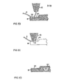
- a "deep puddle bond” is shown in cross section in Fig. 2A where the lead wire 11 has been solidified in a deeper pool originally extending approximately half the depth or thick- ness into the lead frame finger 8.
- the lead wire 11 has hardened and welded into the very surface 24 of lead frame finger 8.
- only a shallow molten pool is required in the latter instance for puddle welding the bonding wire at the surface.
- the energy delivered to surface 24 of the lead frame finger by electrode 20 is controlled to achieve a high temperature but below the melting point of the metal comprising the lead frame finger.
- the electrode 20 is then retracted so that capillary tool 12 may move into position and effect a ther- nocompression wedge bond in which the lower bearing edge 13 of tool 12 applies pressure to the lead wire against the surface 24 of lead frame finger 8 resulting in the wedge bond of Fig. 2C.
- the lead frame finger 8 was first preheated to a temperature approaching but below the melting point of the metal permitting an efficient and effective wedge bond without the necessity for gold or silver plating of the lead frame elements and without the necessity of using gold and silver lead wires.
- a lead frame finger element of the type illustrated in Fig. 2D may be used.
- the lead frame is formed by a core 26 of red brass or copper, coated, bonded or laminated with an outer layer 27 of stainless steel.
- This laminar combination on the lead frame elements provides the dual advantage that a shallow puddle 25 of long life may be formed in the stainless steel layer 27. Heat may still generally be conducted away with high thermal conductivity through the central core 26 of red brass or copper.
- a feature and advantage generally of the molten pool immersion welding method of the present invention referred to herein as "puddle bonding" is that different metals which normally cannot be bonded at the low temperature and energy levels permitted in the vicinity of the microcircuit chip may now be securely welded or bonded together.
- copper wire may be bonded to brass or red brass without the necessity of plating the fingers with gold or silver. Bonding may similarly be effected to stainless steel, nickel, and aluminum by way of example and all without the necessity of plating of the contacting elements.
- lead wires of metals other than silver or gold may be used.
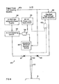
- a suitable electric circuit and power supply for delivering a controlled amount of energy in the form of a controlled pulse train to the puddle forming or enhanced preheating electrode 20, is illustrated in Fig. 4. Electrode 20 is also referred herein as to the zapper electrode.
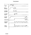
- a timing diagram showing operation of the components of the power supply is illustrated in Fig. 4A.
- the power supply 30 shown in Fig. 4 is a line frequency variable voltage DC power supply delivering DC pulses at 60 Hz in a range of up to for example 750 V. To this end there is provided a 0 to 750 V AC adjustable voltage power supply 32 delivering the sinusoidal AC output designated 32a in timing diagram 4A.
- the 60 Hz power line sync circuit 33 comprising a Schmitt trigger circuit, squares up the sine wave providing the output designated 33a in the timing diagram of Fig. 4A.
- the power line sync circuit output through gate 34 triggers SCR switching circuit 35 consisting of a silicon controlled rectifier.
- Gate 34 however passes the trigger pulses from sync circuit 33 only for the duration during which the adjustable one shot duration control 36 is conducting.
- the one shot monostable multivibrator 36 is adjustable to provide a duration control signal designated 36a in the timing diagram of Fig. 4A for passing a controlled amount of energy of desired quantity measured by the time duration of the signal output 36a.
- the trigger pulses 34a at the output of gate 34 are therefore limited for the duration of the control signal 36a from adjustable one shot 36 as shown in the timing diagram of Fig. 4A.
- the duration control signal 36a from one shot 36 is initiated by the trigger pulse 30a from the bonding machine in which the apparatus and circuitry of the present invention is housed.
- the output from SCR 35 designated signal 35 in the timing diagram of Fig. 4A therefore represents a rectified pulse train of positive pulses derived from the adjustable power supply 32 and of controlled duration determined by the control signal from one shot 36.
- the DC pulse train 35a of controlled duration passes through rectifier 37 to elec-4 trode 20 for arc discharge to the grounded lead frame finger 8 for puddle formation or enhanced preheating as heretofore described.
- a further important element of the power supply is the one shot high voltage spike generator 38 which is actuated at the outset by the trigger pulse 30a from the bonding machine.
- the high voltage spike pulse output 38a. from the voltage spike generator 38 precedes the pulse train 35a to initiate ionization of air between the electrode 20 and lead frame finger 8. While the voltage amplitude of the rectified DC pulses 35a as in the order of up to 750 V, the single preceding ionization spike 38a has a voltage in the order of 4 to 10 KV.
- the voltage spike represents a very high voltage but very low current pulse of energy to initiate an ionized path between electrode 20 and lead frame finger 8 along which the lower voltage higher current pulse train of controlled duration 35a conducts for delivering a controlled amount of energy to the bonding location at the lead frame finger via arc discharge from electrode 20.
- the high voltage spike passes through rectifier 39 to the electrode.
- Rectifiers 37 and 39 isolate the controlled pulse train generating side of the power supply from the initial high voltage spike generating side of the power supply.
- Rectifier 39 can be a solid state rectifier while a vacuum tube rectifier may be necessary for rectifier 37 because of the higher current for delivering energy for electrode 20.
- the combined output 40 applied to electrode 20 is indicated by signal 40a in the timing diagram of Fig. 4A. As there shown, the initial ionization spike precedes the pulse train providing a conductive pathway for the arc discharge of precisely metered energy.
- the line frequency variable voltage DC power supply 30 generates a rectified pulse output using only the positive alternation of the sign wave and gating the pulses with a time duration control signal thereby metering the energy delivered for bonding at the lead frame finger.
- a negative ground is applied at the lead frame finger and electrons jump from the finger to the electrode 20. This may be advantageous where the lead frame finger 8 is at a higher temperature because of the heated work holder on which the lead frame strip is mounted as hereafter described.
- the electron discharge can be effected in either direction according to the present invention.
- the duty cycle of the pulses may be controlled by adding a Jones circuit for forced commutation at selected duty cycles.
- pulsing of energy to the electrode 20 permits more precise control and metering of energy delivered to the bonding location for puddle formation or enhanced preheating.
- delivering energy in the form of a pulse train of controlled duration affords more precise control over the delivered energy than can be achieved by a single pulse or current of variable duration.
- pulse frequency, pulse amplitude, pulse duration and duty cycle may be respectively varled in addition to the overall duration of the pulse train.
- energy in digital form may be more precisely gated according to the present invention.
- an ionizing spike pulse may be necessary before each pulse of the pulse train to maintain ionization of the air between electrode 20 and lead frame finger 8.
- the combination of the delay between pulses at lower frequency and the flow of argon gas directed at the bonding site as hereafter described may blow out the arc. Therefore it may be desirable to include an ionization spike before each pulse when the argon or other inert gas flow reaches a critical level at frequencies of 60 Hz or lower which may extinguish the ionized path.
- a further gate 42 may be introduced into the power supply 30 as shown in dotted outline in Fig. 4.
- One of the inputs to gate 42 is the power line sync circuit output 33a while the other input is the adjustable one shot duration control output 36a.
- the output of gate 42 triggers one shot high voltage spike generator 38 at each pulse of the pulse train during the period of controlled duration defined by the adjustable one shot 36.
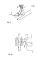
- the electrode support 50 includes a mounting and bearing frame 51 containing a spring 52 which at the lower end 53 bears against the frame 51 and which at the upper end 54 bears against the solenoid plunger 55 connected to the electrode rod 21.
- the frame 51 is formed with a hole 56 through which the electrode 20 is inserted so that the electrode tip 22 projects in the vicinity of the bonding location on lead frame finger 8.
- spring 52 biases the electrode in an outward moving or retracting direction which may be counteracted when solenoid 60 is actuated.
- the work holder 90 (Figs. 6 & 7) includes a lead frame hold down clamp 59 for bearing against the trunk portion of lead frame finger 8 when the electrode and electrode frame 51 have been positioned over the lead frame.
- a feature and advantage of lead frame hold down clamp 59 is that it prevents or attenuates relative motion of Lead frame finger 8 with respect to the heated work holder surface 60 on which the lead frame strip is supported as hereafter further described.
- Relative motion of finger 8 Ln the vertical direction of as much as 1 to 3 mils is otherwise possible significantly varying the spacing between electrode tip 22 and surface 24 of the lead frame finger critical to the delivery of a controlled amount of energy for bonding at the -finger.
- the spacing between electrode tip 22 and surface 24 may be as little as 3 to 5 mils during preparation for a puddle bond or molten pool immersion bond.
- the motion of finger 8 may not be as critical. In either event lead frame hold down clamp 59 prevents significant variation in the electrode to surface spacing.
- the electrode mounting and bearing frame 51 is precisely mounted and controlled on a lever arm coupled to the bonding machine for positioning and indexing of the zapper electrode mounting apparatus over the selected lead frame of a strip supported on the work holder surface 60.
- a bonding machine and work holder modified and adapted in accordance with the present invention is illustrated in Figs. 6 and 7.
- Such a bonding machine 70 of the type described in the Kulicke and Soffa Model 478 Handbook includes a capillary tool holder 72 in which the capillary tool 12 is mounted for positioning over a microcircuit chip and lead frame of the lead frame strip 6 mounted on work holder 60.
- the capillary tool holder 72 is connected by coupling 73a to'lever arm 73 which is in turn connected to the tool control rod 74.
- the tool output links or camming rods 75 and 76 in turn controlled by the bonding machine 70 bear against the tool control rod 74 for alternatively raising and lowering the capillary tool holder 72 for accurate positioning of the capillary tool 12 relative to a particular lead wire bonding location.
- Flameoff electrode 80 pivotally mounted on arm 81 whose rotational position is controlled by a lever arm 82 now shown supported at and coupled to the bonding machine 70.
- Flameoff electrode 80 includes an argon shield 83 for delivering argon or other inert gas to the ball forming arc flameoff site.
- the ball forming flameoff arc electrode is used in the formation of a ball at the end of lead wire 11 held by capillary tool 12 prior to ball bonding of the end of the lead wire to the die pad of an integrated circuit chip mounted on a lead frame of strip 6.
- a further lever arm or rod 85 is adapted from the bonding machine 70 to support the zapper electrode mounting frame 50 and electrode 20 of the type described with reference to F ig. 5.
- This electrode frame holder 85 may be moved up and down in the same manner as tool holder 72.
- Lead wire 58 from electrode 20 extends into the bonding machine 70 where a power supply of the type described in Fig. 4 is housed according to the modification of the bonding machine according to the present invention.
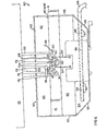
- an argon source 88 is provided for delivering a stream of argon or other inert gas through nozzle 87 into the site of puddle bonding or enhanced preheating welding at a selected lead frame finger.
- the work holder 60 is a lead frame strip work holder of the type manufactured by Kulicke & Soffa Industries, Inc., 507 Prudential Road, Horsham, Pennsylvania 19044, and described in the Model 261 Universal IC/Transistor Workholder Handbook published by Kulick & Soffa.
- a work holder 60 includes a strip guide or track 61 centered between guide rails 62 for feeding and guiding a lead frame strip 6 to the locus of lead wire bonding.
- the center of the work holder may be heated transferring heat to the strip.
- the bonding location is defined by a hold down clamp or ring clamp spring loaded by arms 64 against a particular lead frame of strip 6 centered at the locus of bonding and welding beneath the operative tools and positioning arms e.g. 72, 80, 82, 50, 85, 88 etc. projecting from the bonding machine 70.
- Work holder 60 however has been modified according to the present invention to provide an inert gas enclosure or bowl 90 comprising walls 92 formed around the upper surface and bearing surface of the work holder.
- the guide track 61 and guide rails 62 form the base or floor of the inert gas enclosure 90 with side walls fitted to conform to the periphery of the work holder.
- floor portions 94 are provided attached to the extended wall portions 93 to meet and abut against the existing surfaces 62 of work holder 60.
- the enclosure is not entirely air tight, it need not be provided it defines a substantially argon or other inert gas environment entirely around the region of welding and bonding and provided the inert gas is continually replenished.
- the rear wall.of the enclosure is provided with a cutout portion 95 for receiving the operative bonding tools from bonding machine 70 in the vicinity of ring clamp 63.
- the workholder enclosure is twice as long as a lead frame strip 6 for loading the strip, advancing the strip to the bonding position, and unloading the strip.
- Strips 6 are loaded into and unloaded from the workholder I enclosure 90 through respective slits 99 formed in the walls 92 at the ends of the enclosure.
- a source 96 of inert gas is provided leading to a distribution tube 98 provided and positioned along the side at the base of the enclosure. Distribution holes 97 along the length of the tube 98 assure a complete flooding of the enclosure with inert gas.
- argon source 96 and distribution tube 98 also referred to herein as the first argon source or first inert gas source provide a large volume low pressure source of inert gas for flooding the entire enclosure.
- This arrangement- and function of the first argon source 96 differs substantially from the second argon source 88 and 87 which functions as a nozzle for delivering a lower volume higher pressure and velocity stream of gas directly at the bonding location on the lead frame finger.
- the second argon source 88, 87 assures inert gas protection directly at the high temperature location of welding according to the present invention and also performs a cooling function in efficiently removing heat from the welding zone.
- the first argon source is for flooding the enclosure while the second argon source is for providing a directed stream.
- the entire workholder 60 modified in accordance with the present invention is mounted before the bonding machine 70 on a chessman and base, not shown, which permits universal movement of the workholder 60 beneath the operative bonding tools projecting from the bonding machine.
- the chessman permits precise positioning of the selected microcircuit die pad beneath the capillary tool 12 for ball bonding the end of the lead wire to the die pad, and sub- seuqently for precise positioning of the lead frame finger beneath the zapper electrode 20 in mounting frame 50 for puddle or pool formation or enhanced heating in accordance with the present invention.
- the lead frame finger and bonding location may then be positioned beneath the capillary tool 12 for pool immersion welding and bonding of the wire or for enhanced preheating thermo- compression bonding.
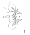
- a lead frame reel-to-reel bonding system 101 is illustrated in Figure 8.
- a bonding machine 70 and workholder 60 with enclosure 90 as described with reference to Figs. 6 and 7 are provided.
- the base 102 on which the chessman and workholder 60 with enclosure 90 are mounted is provided with heavy duty reel mounts or supports 103 and 104 for rotatably supporting and mounting the large diameter heavy weight lead frame reels as shipped from the lead frame manufacturer.
- Lead frame ribbon feed reel 105 feeds a continuous lead frame ribbon 106 through the loading slot 99 of workholder 60 and its enclosure 90 to the welding and bonding working zone within the workholder enclosure.
- the ribbon then passes out the unloading slot and onto the ta k eup reel 108. In this manner the cutting and handling of separate strips is avoided. Because the reels may be used directly from the manufacturer without plating with silver or gold, handling and damage is of course minimized.
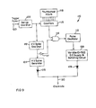
- FIG. 9 An alternative power supply according to the present invention for delivering a controlled pulse train and a precisely metered quantity of energy to the bonding site of a lead frame finger is illustrated in Fig. 9, with a timing diagram showing operation of the components of the power supply presented in Fig. 10.
- metering of the delivered energy is accom- p lished by'counting the pulses of the pulse train and delivering a preset count of electrical pulses.
- a variable frequency power supply 110 is shown in Fig. 9 with a separate pulse oscillator 112 for delivering pulses at an adjustable selected frequency.
- the pulse oscillator 112 which generates the pulse signal 112 of Fig.
- gate 10 is controlled by gate 114 which actuates the pulse oscillator only for the duration of the gate control output signal 114a.
- the gate 114 is in turn jointly controlled by the outputs from the counters 115 and high voltage spike one shot 116 having respective output signal traces 115a and 116a as shown in the timing diagram of Fig. 10.
- the output of one shot 116 is inverted by inverter 117 prior to input to gate 114.
- Thumbwheel inputs 118 are used to set the counters 115 to a preset count for metering the energy ultimately delivered to the electrode 20.
- a trigger pulse 120 from the bonding machine actuates the set up one shot 122 which delivers signal pulse 122a to actuate the counters and high voltage one shot 116.
- the high voltage one shot actuates the high voltage spike generator which delivers the high voltage spike pulse 124a through diode 125 to the electrode 20.
- the output from high voltage spike one shot 116 after inversion and in combination with the counters actuates the pulse oscillator to deliver the preset count of electrical pulses to actuate the variable voltage (e.g. 0-750 V) DC power supply and switching circuit 128 delivering DC pulses through rectifier 129 to the electrode.
- DC power supply 128 is of the type illustrated and described with reference to i Fig. 4.
- the high voltage spike 124 a in combination with the DC pulses 112a provide the mixed output 130 as shown in the timing diagram of Fig. 10.
- the power supply of Figs. 3 and 10 deliver a controlled amount of energy for puddle bonding and enhanced preheating welding according to the present invention by delivering a preset count of electrical pulses. Further details of a similar power supply for delivering a preset count of electrical pulses for metered arc discharge of energy is found in our copending patent application Serial No. 262,595 filed on May 11, 1981 and entitled "Wire Bonding Ball Forming Method & Apparatus", referred to above.
- FIG. 11 Yet another alternative power supply in the form of a fixed line frequency variable voltage power supply is illustrated in Fig. 11.
- This power supply is similar to that described with reference to Fig. 9 except that the fixed line frequency power supply at 60 Hz is used.
- a line sync circuit 132 is added to actuate the counters and the line sync output in combination with the outputs from counter 115 control the gate 134 providing counted pulses to gate the output through SCR 136.
- SCR 136 passes the positive alternation of the output from variable voltage (e.g. 0-750 VAC) AC power supply 138.
- Counted D.C. pulses amounting to a pulse train of a preset count of electrical pulses therefore pass through rectifier 129 to provide a combined output with the high voltage spike in which the spike preceeds the pulse train.
- the high voltage spike generator may comprise a 12 volt DC supply, switching transistor, and induction coil for generating the spike voltage in the range of 4-10 Kv.
- the switching transistor is turned on and shut off by the one shot pulse from one shot multivibrator 116.
- the duty cycle of the pulses of the counted pulse train may be varied.
- the duty cycle is easily controlled at the oscillator.
- the duty cycle can be controlled by adding a Jones circuit for forced commutation.
- the spacing between electrode 20 and lead frame finger 8 Prior to actuation of either of the alternative power supplies by a trigger pulse from the bonding machine the spacing between electrode 20 and lead frame finger 8 is first set and adjusted at the desired spacing by means of a feeler gauge, by means of eye placement through a microscope and reticle associated with the bonding machine, by touching the lead frame finger surface with the electrode to complete an electric circuit then pulling back a specified distance, or by means of test pulses preceeding the high voltage spike and controlled pulse train, etc.
- An electrode two cm. long is provided for purposes of such manipulation.
- a warning indicator may be provided when a circuit is made by unintended contact between the electrode and lead frame.
- the power supplies may be adjusted to yield a variety of temperatures relative to the metals used for the lead wire and lead frame finger.
- the melting point of the lead wire metal may be selected to be higher or lower than the melting temperature of the lead frame finger in which the molten pool or enhanced preheating is effected.
- temperatures in the lead frame finger either below or above the melting point may be achieved according to the bonding method.
- molten pool immersion bonding may be accomplished according to a variety of methods once the molten pool or puddle of desired volume is formed in the lead frame finger.
- the molten pool or puddle is typically no greater than one third to one half the width and thickness of the lead frame finger.
- the wire may be immersed directly into the molten pool thereafter letting the puddle solidify.
- the melting point of the wire it is desirable that the melting point of the wire be higher than the melting point of the lead frame finger metal.
- the wire is pushed ultrasonically into the puddle just as it solidifies. In this event the lead wire metal may have a melting point lower than that of the lead frame finger metal.
- the lead wire can be welded by the capillary tool to the lead frame finger by ultrasonic welding or thermocompression welding just as the finger metal solidifies.
- the weld may be effected after the molten pool or puddle has solidified.
- the dam bar is cooled by a heat sink.
- the surface mass of the workholder on which the lead frame strip is supported can serve this purpose.
- the center portion of such workholder surfaces are presently provided with a heater for which water cooling or other cooling may be substituted for carrying off even more heat energy.
- a thermal mass without water cooling is sufficient.
- the fingers must be electrically isolated from each other to prevent electrical pulses at adjacent fingers from traveling to the chip via previously bonded and welded lead wires.
- the heat sink at the dam bar may also be grounded to accomplish this purpose. As a result all high voltage or high current pulses are discharged at electrically isolated fingers and high energy delivery does not occur at any finger electrically connected to the chip.
Landscapes
- Wire Bonding (AREA)
Applications Claiming Priority (2)
| Application Number | Priority Date | Filing Date | Title |
|---|---|---|---|
| US294411 | 1981-08-19 | ||
| US06/294,411 US4434347A (en) | 1981-08-19 | 1981-08-19 | Lead frame wire bonding by preheating |
Publications (2)
| Publication Number | Publication Date |
|---|---|
| EP0073172A2 true EP0073172A2 (fr) | 1983-03-02 |
| EP0073172A3 EP0073172A3 (fr) | 1985-01-16 |
Family
ID=23133296
Family Applications (1)
| Application Number | Title | Priority Date | Filing Date |
|---|---|---|---|
| EP82401558A Withdrawn EP0073172A3 (fr) | 1981-08-19 | 1982-08-19 | Technique pour connexion de fils pour puces à circuit intégré |
Country Status (8)
| Country | Link |
|---|---|
| US (1) | US4434347A (fr) |
| EP (1) | EP0073172A3 (fr) |
| JP (1) | JPS5842248A (fr) |
| KR (1) | KR840001386A (fr) |
| AU (1) | AU556303B2 (fr) |
| BR (1) | BR8204862A (fr) |
| CA (1) | CA1187626A (fr) |
| MX (1) | MX151763A (fr) |
Cited By (3)
| Publication number | Priority date | Publication date | Assignee | Title |
|---|---|---|---|---|
| DE3606224A1 (de) * | 1985-03-01 | 1986-09-04 | Mitsubishi Denki K.K., Tokio/Tokyo | Kugeltyp-bond-draehte fuer halbleitervorrichtungen und verfahren zu ihrer herstellung |
| WO1993018493A1 (fr) * | 1992-03-03 | 1993-09-16 | N.V. Nederlandsche Apparatenfabriek Nedap | Procede de fabrication d'une etiquette de detection a hautes frequences avec un minimum de composants electroniques |
| US10381708B2 (en) | 2017-10-30 | 2019-08-13 | International Business Machines Corporation | Superconducting resonator to limit vertical connections in planar quantum devices |
Families Citing this family (36)
| Publication number | Priority date | Publication date | Assignee | Title |
|---|---|---|---|---|
| JPS6189643A (ja) * | 1984-10-09 | 1986-05-07 | Toshiba Corp | 半導体装置及びその製造方法 |
| US4717066A (en) * | 1986-02-24 | 1988-01-05 | American Telephone And Telegraph Company, At&T Bell Laboratories | Method of bonding conductors to semiconductor devices |
| JPH0699756B2 (ja) * | 1986-06-26 | 1994-12-07 | 新日本製鐵株式会社 | 高強度高r値冷延鋼板の製造方法 |
| US5059559A (en) * | 1987-11-02 | 1991-10-22 | Hitachi, Ltd. | Method of aligning and bonding tab inner leads |
| JPH03136340A (ja) * | 1989-10-23 | 1991-06-11 | Shinkawa Ltd | ワイヤボンデイング方法及び装置 |
| JPH05226407A (ja) * | 1991-11-12 | 1993-09-03 | Nec Corp | 半導体装置の製造方法及び製造装置 |
| US7073254B2 (en) * | 1993-11-16 | 2006-07-11 | Formfactor, Inc. | Method for mounting a plurality of spring contact elements |
| US20020053734A1 (en) * | 1993-11-16 | 2002-05-09 | Formfactor, Inc. | Probe card assembly and kit, and methods of making same |
| US5495667A (en) * | 1994-11-07 | 1996-03-05 | Micron Technology, Inc. | Method for forming contact pins for semiconductor dice and interconnects |
| US5954842A (en) * | 1996-01-26 | 1999-09-21 | Micron Technology, Inc. | Lead finger clamp assembly |
| US5647528A (en) | 1996-02-06 | 1997-07-15 | Micron Technology, Inc. | Bondhead lead clamp apparatus and method |
| US5890644A (en) | 1996-01-26 | 1999-04-06 | Micron Technology, Inc. | Apparatus and method of clamping semiconductor devices using sliding finger supports |
| US5673845A (en) | 1996-06-17 | 1997-10-07 | Micron Technology, Inc. | Lead penetrating clamping system |
| US8033838B2 (en) * | 1996-02-21 | 2011-10-11 | Formfactor, Inc. | Microelectronic contact structure |
| US5994152A (en) | 1996-02-21 | 1999-11-30 | Formfactor, Inc. | Fabricating interconnects and tips using sacrificial substrates |
| US6068174A (en) * | 1996-12-13 | 2000-05-30 | Micro)N Technology, Inc. | Device and method for clamping and wire-bonding the leads of a lead frame one set at a time |
| US6121674A (en) * | 1998-02-23 | 2000-09-19 | Micron Technology, Inc. | Die paddle clamping method for wire bond enhancement |
| US6126062A (en) * | 1998-04-02 | 2000-10-03 | Micron Technology, Inc. | Non-conductive and self-leveling leadframe clamp insert for wirebonding integrated circuits |
| US6634538B2 (en) | 1998-04-02 | 2003-10-21 | Micron Technology, Inc. | Non-conductive and self-leveling leadframe clamp insert for wirebonding integrated circuits |
| US6031216A (en) * | 1998-06-17 | 2000-02-29 | National Semiconductor Corporation | Wire bonding methods and apparatus for heat sensitive metallization using a thermally insulated support portion |
| US6158647A (en) | 1998-09-29 | 2000-12-12 | Micron Technology, Inc. | Concave face wire bond capillary |
| US6977214B2 (en) * | 1998-12-11 | 2005-12-20 | Micron Technology, Inc. | Die paddle clamping method for wire bond enhancement |
| EP1306898A1 (fr) * | 2001-10-29 | 2003-05-02 | Dialog Semiconductor GmbH | Sous-milliohm interconnexion sur puce |
| US20030146500A1 (en) * | 2002-02-04 | 2003-08-07 | Stmicroelectronics S.R.L. | Package for semiconductor device with ground lead connection having high stress resistance |
| US7404513B2 (en) * | 2004-12-30 | 2008-07-29 | Texas Instruments Incorporated | Wire bonds having pressure-absorbing balls |
| DE102005043413A1 (de) * | 2005-09-13 | 2007-03-15 | Robert Bosch Gmbh | Grundmodul für einen Bewegungssensor |
| EP2091684A1 (fr) | 2006-11-07 | 2009-08-26 | Perkinelmer Optoelectronics GmbH & Co. Kg | Méthode pour assembler des surfaces métalliques pour application d'une première couche de métal oxydé et d'une deuxième couche de métal oxydé; objet ayant des cavités ou structure d'une diode émettant de la lumière produits par cette méthode |
| US20080197461A1 (en) * | 2007-02-15 | 2008-08-21 | Taiwan Semiconductor Manufacturing Co.,Ltd. | Apparatus for wire bonding and integrated circuit chip package |
| DE202007008706U1 (de) * | 2007-06-19 | 2007-09-13 | Ultrasonics Steckmann Gmbh | Ultraschall-Schweißstation |
| US20090014499A1 (en) * | 2007-07-11 | 2009-01-15 | Honeywell International Inc. | Automated preform attach for vacuum packaging |
| WO2011052653A1 (fr) * | 2009-10-29 | 2011-05-05 | 日本電業工作株式会社 | Appareil de régénération de puissance, procédé de régénération de puissance, système de stockage de puissance, procédé de stockage de puissance, et appareil haute fréquence |
| CN104215235B (zh) * | 2013-06-05 | 2017-08-22 | 北京信息科技大学 | 一种新型钟形振子式角速率陀螺 |
| CN104084659B (zh) * | 2014-07-02 | 2016-04-20 | 佛山市施翔腾科技设备有限公司 | 采用热风焊接方法制备晶体管的生产方法 |
| JP6463300B2 (ja) * | 2016-05-20 | 2019-01-30 | 矢崎総業株式会社 | 端子化電線製造方法 |
| US10818514B1 (en) * | 2017-07-14 | 2020-10-27 | Triad National Security, Llc | Fine wire manipulator |
| JP6633719B1 (ja) * | 2018-11-07 | 2020-01-22 | 電元社トーア株式会社 | インバータ電源装置 |
Family Cites Families (5)
| Publication number | Priority date | Publication date | Assignee | Title |
|---|---|---|---|---|
| US3409977A (en) | 1963-10-28 | 1968-11-12 | Texas Instruments Inc | Hot gas thermo-compression bonding |
| JPS4919634B1 (fr) * | 1969-12-29 | 1974-05-18 | ||
| FR2160764A1 (en) * | 1971-11-26 | 1973-07-06 | Radiotechnique Compelec | Semiconductor component prodn machine - with thermocompression welder |
| GB1600021A (en) | 1977-07-26 | 1981-10-14 | Welding Inst | Electrical inter-connection method and apparatus |
| DE2919998A1 (de) * | 1979-05-17 | 1980-11-27 | Siemens Ag | Befestigen der anschlussdraehte von halbleitersystemen auf den traegerelementen |
-
1981
- 1981-08-19 US US06/294,411 patent/US4434347A/en not_active Expired - Fee Related
-
1982
- 1982-08-18 KR KR1019820003705A patent/KR840001386A/ko not_active Withdrawn
- 1982-08-18 AU AU87281/82A patent/AU556303B2/en not_active Ceased
- 1982-08-18 CA CA000409698A patent/CA1187626A/fr not_active Expired
- 1982-08-18 MX MX194051A patent/MX151763A/es unknown
- 1982-08-19 JP JP57142730A patent/JPS5842248A/ja active Pending
- 1982-08-19 EP EP82401558A patent/EP0073172A3/fr not_active Withdrawn
- 1982-08-19 BR BR8204862A patent/BR8204862A/pt unknown
Cited By (3)
| Publication number | Priority date | Publication date | Assignee | Title |
|---|---|---|---|---|
| DE3606224A1 (de) * | 1985-03-01 | 1986-09-04 | Mitsubishi Denki K.K., Tokio/Tokyo | Kugeltyp-bond-draehte fuer halbleitervorrichtungen und verfahren zu ihrer herstellung |
| WO1993018493A1 (fr) * | 1992-03-03 | 1993-09-16 | N.V. Nederlandsche Apparatenfabriek Nedap | Procede de fabrication d'une etiquette de detection a hautes frequences avec un minimum de composants electroniques |
| US10381708B2 (en) | 2017-10-30 | 2019-08-13 | International Business Machines Corporation | Superconducting resonator to limit vertical connections in planar quantum devices |
Also Published As
| Publication number | Publication date |
|---|---|
| AU556303B2 (en) | 1986-10-30 |
| KR840001386A (ko) | 1984-04-30 |
| CA1187626A (fr) | 1985-05-21 |
| US4434347A (en) | 1984-02-28 |
| MX151763A (es) | 1985-03-05 |
| EP0073172A3 (fr) | 1985-01-16 |
| BR8204862A (pt) | 1983-08-02 |
| AU8728182A (en) | 1983-02-24 |
| JPS5842248A (ja) | 1983-03-11 |
Similar Documents
| Publication | Publication Date | Title |
|---|---|---|
| US4434347A (en) | Lead frame wire bonding by preheating | |
| US6234376B1 (en) | Supplying a cover gas for wire ball bonding | |
| US4909427A (en) | Bonding wire ball formation | |
| KR960009982B1 (ko) | 와이어 본딩 방법 및 와이어 본딩 장치 및 그 와이어 본딩 방법에 의해 생산되는 반도체 장치 | |
| CA1199126A (fr) | Methode et appareil de formation de billes de fil | |
| US4039700A (en) | Hard metal coating process for metal objects | |
| US4950866A (en) | Method and apparatus of bonding insulated and coated wire | |
| US8096461B2 (en) | Wire-bonding machine with cover-gas supply device | |
| US5295619A (en) | Method and apparatus for performing wire bonding by using solder wire | |
| EP0541116B1 (fr) | Procédé pour la liaison d'un conducteur et d'une électrode d'un dispositif électronique | |
| US4323759A (en) | Electrical inter-connection method | |
| GB1536872A (en) | Electrical inter-connection method and apparatus | |
| US10399170B2 (en) | Die attachment apparatus and method utilizing activated forming gas | |
| US6337453B1 (en) | Method and apparatus for arc-forming a bonding wire ball with attenuated electro-magnetic interference | |
| US4476366A (en) | Controlled bonding wire ball formation | |
| EP0111427B1 (fr) | Régulation de la formation d'une boule de liaison par un gaz de couverture | |
| JPS62276840A (ja) | ボンデイング装置 | |
| JPS60134444A (ja) | バンプ電極形成方法 | |
| JPH03253045A (ja) | ワイヤボンディング装置 | |
| JPH0536748A (ja) | ワイヤボンデイング装置 | |
| US6739494B2 (en) | Device with electrodes for the formation of a ball at the end of a wire | |
| JP2504855B2 (ja) | 配線の製造方法 | |
| JPH01256134A (ja) | ワイヤボンディング装置 | |
| JPH01256135A (ja) | ワイヤボンディング装置 | |
| JP2781213B2 (ja) | バンプの形成方法 |
Legal Events
| Date | Code | Title | Description |
|---|---|---|---|
| PUAI | Public reference made under article 153(3) epc to a published international application that has entered the european phase |
Free format text: ORIGINAL CODE: 0009012 |
|
| AK | Designated contracting states |
Designated state(s): CH DE FR GB IT LI |
|
| PUAL | Search report despatched |
Free format text: ORIGINAL CODE: 0009013 |
|
| AK | Designated contracting states |
Designated state(s): CH DE FR GB IT LI |
|
| 17P | Request for examination filed |
Effective date: 19850610 |
|
| 17Q | First examination report despatched |
Effective date: 19870626 |
|
| STAA | Information on the status of an ep patent application or granted ep patent |
Free format text: STATUS: THE APPLICATION IS DEEMED TO BE WITHDRAWN |
|
| 18D | Application deemed to be withdrawn |
Effective date: 19871107 |
|
| RIN1 | Information on inventor provided before grant (corrected) |
Inventor name: KURTZ, JOHN A. Inventor name: COUSENS, DONALD E. |