EP0074604B1 - Circuit utilisant l'effet Josephson - Google Patents
Circuit utilisant l'effet Josephson Download PDFInfo
- Publication number
- EP0074604B1 EP0074604B1 EP82108223A EP82108223A EP0074604B1 EP 0074604 B1 EP0074604 B1 EP 0074604B1 EP 82108223 A EP82108223 A EP 82108223A EP 82108223 A EP82108223 A EP 82108223A EP 0074604 B1 EP0074604 B1 EP 0074604B1
- Authority
- EP
- European Patent Office
- Prior art keywords
- resistor
- input
- josephson junction
- circuit
- current
- Prior art date
- Legal status (The legal status is an assumption and is not a legal conclusion. Google has not performed a legal analysis and makes no representation as to the accuracy of the status listed.)
- Expired
Links
Images


Classifications
-
- H—ELECTRICITY
- H03—ELECTRONIC CIRCUITRY
- H03K—PULSE TECHNIQUE
- H03K19/00—Logic circuits, i.e. having at least two inputs acting on one output; Inverting circuits
- H03K19/02—Logic circuits, i.e. having at least two inputs acting on one output; Inverting circuits using specified components
- H03K19/195—Logic circuits, i.e. having at least two inputs acting on one output; Inverting circuits using specified components using superconductive devices
- H03K19/1954—Logic circuits, i.e. having at least two inputs acting on one output; Inverting circuits using specified components using superconductive devices with injection of the control current
- H03K19/1956—Logic circuits, i.e. having at least two inputs acting on one output; Inverting circuits using specified components using superconductive devices with injection of the control current using an inductorless circuit
-
- Y—GENERAL TAGGING OF NEW TECHNOLOGICAL DEVELOPMENTS; GENERAL TAGGING OF CROSS-SECTIONAL TECHNOLOGIES SPANNING OVER SEVERAL SECTIONS OF THE IPC; TECHNICAL SUBJECTS COVERED BY FORMER USPC CROSS-REFERENCE ART COLLECTIONS [XRACs] AND DIGESTS
- Y10—TECHNICAL SUBJECTS COVERED BY FORMER USPC
- Y10S—TECHNICAL SUBJECTS COVERED BY FORMER USPC CROSS-REFERENCE ART COLLECTIONS [XRACs] AND DIGESTS
- Y10S505/00—Superconductor technology: apparatus, material, process
- Y10S505/825—Apparatus per se, device per se, or process of making or operating same
- Y10S505/856—Electrical transmission or interconnection system
- Y10S505/857—Nonlinear solid-state device system or circuit
- Y10S505/858—Digital logic
- Y10S505/859—Function of and, or, nand, nor or not
Definitions
- the present invention relates to circuits utilizing the Josephson effect and, more particularly, to such a logic gate which has very short gate delay time and wide operational margins and is feasible for a high degree of integration.
- One input l a is coupled to the node between the inductances L 1 and L 2 and the other I b to one end of the inductance L 1 .
- the inductance values L 1 ' and L 2 ' and the critical currents 1 01 and 1 02 are chosen to satisfy equations: where ⁇ 0 indicates a natural constant called "magnetic flux quantum" and having a value of the order of 2.07 pH - mA.
- this logic gate is disadvantageous in various respects.
- the critical current should be small for reduction of the power dissipation as seen from the equation (2), the current 1 02 and the inductance values L 1 ' and L 2 ' cannot be reduced at the same time so that a large chip area is required to attain the low power dissipation. Since the gate includes both inductances and Josephson junction capacitance, resonance phenomena is caused which should be damped for high speed operations. Furthermore, a gate of this kind tends to trap stray magnetic field when switching to its superconducting state; the trapped magnetic field would cause the gate to malfunction.
- U.S. Patent No. 4,275,314 discloses an AND gate which is not provided with any inductance component to eliminate the drawbacks discussed above.
- the AND gate uses the circuit indicated in Figure 1 (named JAWS) as a one-input OR gate and cascades two such OR gates.
- the first bias current fed to the first stage JAWS is coupled to the second stage JAWS as the second bias current.
- the second bias current is steered to the output side.
- the turn-on delay time decreases in inverse proportion to the overdrive capability (defined by (I 0 ⁇ I th )/I 0 where 1 0 is the input current and I lh the threshold current for a predetermined gate current).
- the overdrive capability increases with the input sensitivity which is defined by an inclination of a control characteristic line of the gate while the buildup time decreases as the input sensitivity becomes higher.
- the input sensitivity of the above-mentioned gate is 1 which is relatively low to promote high speed switching.
- an AND gate having two or more input lines, or a logic gate having a plurality of input lines and producing an output when input currents flow through a predetermined number or more of the input lines, e.g. a 2/3 logic gate in which an output appears when input currents flow through two or more of three input lines.
- a gate current is constantly fed to the Josephson junctions J 1 and J 2 through the inductances L 1 and L 2 of the interferometer gate, respectively, and the critical currents are selected such that the gate switches in response to the flow of input currents through two or more of the three input lines.
- a circuit comprising a first resistor, a second resistor and a third resistor having predetermined resistances r l , r 2 , r 3 , respectively, and connected together at one end thereof, a first Josephson junction and a second Josephson junction having predetermined critical currents 1 01 and 1 02 , respectively, and connected at one end to the other end of the first and second resistors, respectively, and a third Josephson junction having a predetermined critical current 1 0 and connected at one end to the other end of the third resistor the other ends of said Josephson junctions being connected to a common reference potential.
- Such a circuit has an AND function whereby an output current may be derived from the node between the third resistor and the third Josephson junction when the first and second input currents are supplied at the same time, and it has an amplifying function whereby a predetermined gate current is constantly supplied from the other end of the second resistor and an output, which is an amplified version of an input current from the other end of the first resistor, appears at the node between the third resistor and the third Josephson junction.
- a circuit utilizing the Josephson effect and having the multi-input AND function in which one or more further resistors are additionally connected at one end thereof to the node at which the first, second and third resistors are connected together, and a corresponding number of further Josephson junctions with a predetermined critical current are connected between the other end of a respective one of said further resistors and a common reference potential.
- MZN M/N logic gate
- circuits comprising a first resistor and a second resistor connected together at one end thereof and having predetermined resistances, respectively a first Josephson junction and a second Josephson junction connected at one end to the other end of the first and second resistors, respectively, and having predetermined critical currents, a third Josephson junction having a predetermined critical current and connected at one end to the junction of the first and second resistors, and a third resistor connected between the other end of the first and second resistors and having a predetermined resistance, the other end of said Josephson junctions being connected to a common reference potential.
- Such a circuit may have an AND function whereby an output appears at the node between the third Josephson junction and the first and second resistors when input currents are supplied to the other end of the first and second resistors at the same time, and may have an amplifying function whereby a predetermined gate current is caused to constantly flow from the other end of the second resistor and an output, which is an amplified version of an input current from the other end of the first resistor, appears at the node between the third Josephson junction and the first and second resistor.
- FIG. 1A of the drawings an example of a two-input AND gate is illustrated.
- the AND gate shown includes three resistors R 1 , R 2 , and R 3 which are connected in Y configuration about a node C.
- Josephson junctions J 1 and J 2 are connected between the resistors R 1 and R 2 , respectively and ground.
- a Josephson junction J 3 is connected between the resistor R 3 and ground while a load resistor R L is connected through an output line in parallel with the Josephson junction J 3 .
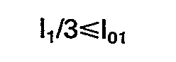
- Critical currents O 01 , 1 02 and I 03 of the Josephson junctions, Jl, J 2 and J 3 and resistances r 1 , r 2 and r 3 of the resistors R 1 , R 2 and R 3 are individually selected to satisfy relations:
- Figure 1B is a graph showing control characteristics of the logic gate provided by the relations (5), (6), (7) and (8) and their versions with I a and I b interchanged.
- the logic gate of this embodiment has wide operational margins and, as will be seen from Figure 1 B, its input sensitivity is as high as 3 which promotes high speed switching. Furthermore, in the logic gate according to this embodiment, there is no limitation as indicated by the equation (2), but the Josephson critical currents and resistances need only to satisfy the relations (3) and (4).
- the logic gate on the substrate therefore, can be designed very small to the ability of lithography. The absence of inductances eliminates the resonance due to the Josephson junction capacitance and requires no additional provision against resonance in the circuit design. Since the logic gate is not of the superconducting loop type, it would not be affected in operation even when trapped stray magnetic fields in the ground plane.
- the current injection type logic gate of this embodiment is also usable as a current amplifier due to its high gain characteristic. An amplifier application will be described with reference to Figure 2.
- a predetermined current I 9 is constantly caused to flow from an input terminal 21. Considering the margins, the current I 9 is preset to 75% of 31 0 . The operation point, therefore, may be the one indicated by 12 in the control characteristic shown in Figure 1B.
- the minimum input current I a required for the transition of the logic gate to the voltage state is 0.25 I 0 .
- the logic gate will provide an output current expressed as 31 0 ⁇ 0.75+0.251 0 which in turn provide a current gain of 10.
- the input current I a will be set at a larger value than 0.251 0 in consideration of the margins and, accordingly, the operation point of the gate circuit under the voltage state will be the one corresponding to 13 shown in Figure 1B.
- logic gate of the present invention is constructed to produce an output when input currents are supplied through a predetermined number or more of a plurality (three or more) of input lines.
- FIG. 3A there is shown a 2/3 logic gate which has input terminals 30, 31 and 32 and produces an output at the load resistor R L when input currents are supplied to two or more of the three input terminals.
- the logic gate shown in Figure 3A is constructed by connecting one end of a resistor R 4 to the node C of the AND gate indicated in Figure 1A and connecting a Josephson junction J 4 between the other end of the resistor R 4 and ground. It will be seen that a logic gate with four or more inputs can be designed as desired employing the same concept.
- the logic gate shown in Figure 3A will be operated as follows.
- the Josephson junctions J 1 , J 2 , J 3 and J 4 are assumed to be common in critical current 1 1 and the resistors R 1 , R 2 , R 3 and R 4 common in resistance.
- I a and 1 l are chosen to have relations:
- the input terminal 31 is supplied with the input current I b which meets a condition: Then, the Josephson junction J 4 is switched to the voltage state so that the input currents I a and I b are individually bisected and steered into the Josephson junctions J 2 and J 3 . At this instant, the Josephson junctions J 2 and J 3 become switched to the voltage state if there holds a relation: This allows the composite input current l a +l b to flow out into the output line which terminates at the load resistor R L .
- the other input current I c may thereafter be injected through the input terminal 32, it is simply steered into the output line through the resistors R 2 and R 3 because all the Josephson junctions J 1 , J 2 , J 3 and J 4 have been switched to the voltage state. As a result, the input current I a +I b +I c is coupled to the load resistor R L through an output line. The same operation procedure, except for the interchange of I a and I b , will occur when I b is injected into the logic gate before l a .
- FIG. 3A The resulting control characteristics of the logic gate shown in Figure 3A is graphically represented in Figure 3B.
- the hatched area of the graph indicates the voltage state of the logic gate. While the input currents I a and I b have been assumed to be coupled to the logic circuit before the input current I c , it will be understood that the control characteristics shown in Figure 3 also applies to a case wherein the currents I a and I c are supplied before the current I b or a case wherein the currents I b and I c are supplied before the current I a , except for the substitution of I a and I b by I a and I c or by I b and I c .
- the logic gate shown in Figure 3A is properly operable as long as the magnitude I 0 of the input currents l a , I b and I c is in a relation:
- the margins of the input current is as wide as 21 1 ⁇ 50%.
- the margins of the input current of the prior art 2/3 logic gate which relies on an interferometer is not more than 0.751 t ⁇ 33.3%.
- the logic gate is fully symmetrical in structure with respect to the input currents I a , I b and I c , and requires no attention to the uniformity of the magnetic coupling between input currents and inductances, so that the complex device design is avoided.
- the absence of inductances as described in relation with Figure 1A permits the logic gate of Figure 3A to be made small, highly integrated and freed from an implement against resonance.
- FIG. 4A a further embodiment of the present invention is shown which is an AND gate having two input terminals.
- the AND gate in Figure 4A is essentially similar to the AND gate in Figure 1A except that the resistor R 3 is omitted and replaced by a resistor R 5 which is connected between two input terminals.
- the AND gate comprises Josephson junctions J 1 , J 2 and J 5 having critical currents I 01 , I 02 and I 05 , resistors R 1 , R 2 and R 5 having resistances r 1 , r 2 and r 5 , a load resistor R L having a resistance r L , and input terminals 40 and 41 to be supplied with input currents I a and I b , respectively.
- the critical currents I 01 , 1 02 and I 05 and the resistance r 1 , r 2 and r 5 are individually chosen to satisfy relations:
- the condition (18) brings the Josephson junction J 2 into the voltage state to allow the input currents I a and I b to be injected into the Josephson junction J 5 .
- the condition (19) then brings the Josephson junction J 5 into the voltage state so that the input currents I a and I b are steered through an output line to the load resistor R L .
- the supply of the input current I b occurs before that of the input current I a , the above description will also apply if I a and I b are replaced by each other.
- the AND gate of Figure 4A has wide operational margins and is capable of high speed switching. It is apparent that all the advantages discussed in connection with the circuitry of Figure 1A are applicable to the circuitry of Figure 4A.
- the logic gate shown in Figure 4A is also usable as a current amplifier due to its high gain characteristic.
- a predetermined current 1 9 is constantly caused to flow from an input terminal 51.
- the current I 9 is preset to 75% of 31 0 .
- the operation point under this condition may be the one indicated by the numeral 42 in Figure 4B.
- the minimum input current I a from an input terminal 50 required for the transition of the logic gate to the voltage state is 0.251 0 .
- the logic gate will provide an output current expressed as 31 0 ⁇ 0.75+0.251 0 which in turn provide a current gain of 10.
- the input current I a will be set at a larger value than 0.251 0 in consideration of the margins and, accordingly, the operation point of the gate circuit under the voltage state will be the one corresponding to 43 shown in Figure 5.
Landscapes
- Engineering & Computer Science (AREA)
- Power Engineering (AREA)
- Physics & Mathematics (AREA)
- Computer Hardware Design (AREA)
- Computing Systems (AREA)
- General Engineering & Computer Science (AREA)
- Mathematical Physics (AREA)
- Logic Circuits (AREA)
- Electronic Switches (AREA)
- Superconductor Devices And Manufacturing Methods Thereof (AREA)
Claims (16)




Applications Claiming Priority (6)
| Application Number | Priority Date | Filing Date | Title |
|---|---|---|---|
| JP56142748A JPS5843630A (ja) | 1981-09-10 | 1981-09-10 | ジヨセフソン効果を用いた電流注入型論理ゲ−ト回路 |
| JP56142749A JPS5843631A (ja) | 1981-09-10 | 1981-09-10 | ジヨセフソン効果を用いた電流注入型論理ゲ−ト回路 |
| JP142748/81 | 1981-09-10 | ||
| JP142749/81 | 1981-09-10 | ||
| JP145313/81 | 1981-09-14 | ||
| JP56145313A JPS5846726A (ja) | 1981-09-14 | 1981-09-14 | ジヨセフソン効果を用いた電流注入型論理ゲ−ト回路 |
Publications (3)
| Publication Number | Publication Date |
|---|---|
| EP0074604A2 EP0074604A2 (fr) | 1983-03-23 |
| EP0074604A3 EP0074604A3 (en) | 1983-05-04 |
| EP0074604B1 true EP0074604B1 (fr) | 1985-12-27 |
Family
ID=27318501
Family Applications (1)
| Application Number | Title | Priority Date | Filing Date |
|---|---|---|---|
| EP82108223A Expired EP0074604B1 (fr) | 1981-09-10 | 1982-09-07 | Circuit utilisant l'effet Josephson |
Country Status (5)
| Country | Link |
|---|---|
| US (1) | US4538077A (fr) |
| EP (1) | EP0074604B1 (fr) |
| AU (1) | AU553981B2 (fr) |
| CA (1) | CA1189916A (fr) |
| DE (1) | DE3268138D1 (fr) |
Families Citing this family (4)
| Publication number | Priority date | Publication date | Assignee | Title |
|---|---|---|---|---|
| JP2679462B2 (ja) * | 1991-08-06 | 1997-11-19 | 日本電気株式会社 | 超伝導回路とその駆動方法 |
| US5170080A (en) * | 1991-08-14 | 1992-12-08 | Westinghouse Electric Corp. | Superconducting push-pull flux quantum digital logic circuits |
| US8571614B1 (en) | 2009-10-12 | 2013-10-29 | Hypres, Inc. | Low-power biasing networks for superconducting integrated circuits |
| US10222416B1 (en) | 2015-04-14 | 2019-03-05 | Hypres, Inc. | System and method for array diagnostics in superconducting integrated circuit |
Family Cites Families (4)
| Publication number | Priority date | Publication date | Assignee | Title |
|---|---|---|---|---|
| US4274015A (en) * | 1978-12-29 | 1981-06-16 | International Business Machines Corporation | Self-resetting Josephson digital current amplifier |
| US4275314A (en) * | 1979-04-30 | 1981-06-23 | Bell Telephone Laboratories, Incorporated | Josephson Atto-Weber switch |
| US4313066A (en) * | 1979-08-20 | 1982-01-26 | International Business Machines Corporation | Direct coupled nonlinear injection Josephson logic circuits |
| US4413196A (en) * | 1981-08-31 | 1983-11-01 | Sperry Corporation | Three Josephson junction direct coupled isolation circuit |
-
1982
- 1982-09-07 DE DE8282108223T patent/DE3268138D1/de not_active Expired
- 1982-09-07 EP EP82108223A patent/EP0074604B1/fr not_active Expired
- 1982-09-08 US US06/415,877 patent/US4538077A/en not_active Expired - Lifetime
- 1982-09-10 AU AU88311/82A patent/AU553981B2/en not_active Ceased
- 1982-09-10 CA CA000411147A patent/CA1189916A/fr not_active Expired
Also Published As
| Publication number | Publication date |
|---|---|
| AU8831182A (en) | 1983-03-17 |
| AU553981B2 (en) | 1986-07-31 |
| EP0074604A2 (fr) | 1983-03-23 |
| CA1189916A (fr) | 1985-07-02 |
| EP0074604A3 (en) | 1983-05-04 |
| US4538077A (en) | 1985-08-27 |
| DE3268138D1 (en) | 1986-02-06 |
Similar Documents
| Publication | Publication Date | Title |
|---|---|---|
| US5455519A (en) | Josephson logic circuit | |
| EP0074604B1 (fr) | Circuit utilisant l'effet Josephson | |
| EP0074666B1 (fr) | Circuit utilisant l'effet Josephson | |
| JP4066012B2 (ja) | 超電導ドライバ回路及び超電導機器 | |
| GB2078046A (en) | Superconductive logic circuit | |
| EP0069534B1 (fr) | Circuit logique supra-conducteur | |
| US4559459A (en) | High gain non-linear threshold input Josephson junction logic circuit | |
| US5389837A (en) | Superconducting flux flow digital circuits | |
| EP0087764B1 (fr) | Générateur d'impulsions de Josephson commandé par courant injecté | |
| JP2550587B2 (ja) | ジヨセフソンゲ−ト | |
| JP2004072219A (ja) | 超電導分周回路 | |
| JP2783032B2 (ja) | ジョセフソン逆流電流防止回路 | |
| JPS622732B2 (fr) | ||
| JP2674652B2 (ja) | ジョセフソン論理セルゲート | |
| JPH0563554A (ja) | 超伝導集積回路 | |
| JPS6334656B2 (fr) | ||
| Yamada et al. | An experimental 4RTD logic gate | |
| JPH0234530B2 (fr) | ||
| JPH07221632A (ja) | ジョセフソン論理回路 | |
| JPH0460373B2 (fr) | ||
| JPH047131B2 (fr) | ||
| JPH06334512A (ja) | ジョセフソン磁界結合型多入力論理和回路 | |
| JPH023327B2 (fr) | ||
| JPH03198387A (ja) | 超伝導回路 | |
| JPH05191253A (ja) | ジョセフソン極性切換型駆動回路 |
Legal Events
| Date | Code | Title | Description |
|---|---|---|---|
| PUAI | Public reference made under article 153(3) epc to a published international application that has entered the european phase |
Free format text: ORIGINAL CODE: 0009012 |
|
| PUAL | Search report despatched |
Free format text: ORIGINAL CODE: 0009013 |
|
| AK | Designated contracting states |
Designated state(s): DE FR GB IT NL |
|
| AK | Designated contracting states |
Designated state(s): DE FR GB IT NL |
|
| RAP1 | Party data changed (applicant data changed or rights of an application transferred) |
Owner name: NEC CORPORATION |
|
| 17P | Request for examination filed |
Effective date: 19831103 |
|
| GRAA | (expected) grant |
Free format text: ORIGINAL CODE: 0009210 |
|
| AK | Designated contracting states |
Designated state(s): DE FR GB IT NL |
|
| ET | Fr: translation filed | ||
| REF | Corresponds to: |
Ref document number: 3268138 Country of ref document: DE Date of ref document: 19860206 |
|
| ITF | It: translation for a ep patent filed | ||
| PLBE | No opposition filed within time limit |
Free format text: ORIGINAL CODE: 0009261 |
|
| STAA | Information on the status of an ep patent application or granted ep patent |
Free format text: STATUS: NO OPPOSITION FILED WITHIN TIME LIMIT |
|
| 26N | No opposition filed | ||
| ITTA | It: last paid annual fee | ||
| PGFP | Annual fee paid to national office [announced via postgrant information from national office to epo] |
Ref country code: GB Payment date: 19940906 Year of fee payment: 13 |
|
| PGFP | Annual fee paid to national office [announced via postgrant information from national office to epo] |
Ref country code: FR Payment date: 19940916 Year of fee payment: 13 |
|
| PGFP | Annual fee paid to national office [announced via postgrant information from national office to epo] |
Ref country code: NL Payment date: 19940930 Year of fee payment: 13 |
|
| PGFP | Annual fee paid to national office [announced via postgrant information from national office to epo] |
Ref country code: DE Payment date: 19941124 Year of fee payment: 13 |
|
| PG25 | Lapsed in a contracting state [announced via postgrant information from national office to epo] |
Ref country code: GB Effective date: 19950907 |
|
| PG25 | Lapsed in a contracting state [announced via postgrant information from national office to epo] |
Ref country code: NL Effective date: 19960401 |
|
| GBPC | Gb: european patent ceased through non-payment of renewal fee |
Effective date: 19950907 |
|
| PG25 | Lapsed in a contracting state [announced via postgrant information from national office to epo] |
Ref country code: FR Effective date: 19960531 |
|
| PG25 | Lapsed in a contracting state [announced via postgrant information from national office to epo] |
Ref country code: DE Effective date: 19960601 |
|
| NLV4 | Nl: lapsed or anulled due to non-payment of the annual fee |
Effective date: 19960401 |
|
| REG | Reference to a national code |
Ref country code: FR Ref legal event code: ST |