EP0075470A2 - Elektronisches Bildverarbeitungssystem - Google Patents
Elektronisches Bildverarbeitungssystem Download PDFInfo
- Publication number
- EP0075470A2 EP0075470A2 EP82304932A EP82304932A EP0075470A2 EP 0075470 A2 EP0075470 A2 EP 0075470A2 EP 82304932 A EP82304932 A EP 82304932A EP 82304932 A EP82304932 A EP 82304932A EP 0075470 A2 EP0075470 A2 EP 0075470A2
- Authority
- EP
- European Patent Office
- Prior art keywords
- pixel
- memory
- image
- pixels
- addressing
- Prior art date
- Legal status (The legal status is an assumption and is not a legal conclusion. Google has not performed a legal analysis and makes no representation as to the accuracy of the status listed.)
- Granted
Links
Images

Classifications
-
- G—PHYSICS
- G06—COMPUTING OR CALCULATING; COUNTING
- G06F—ELECTRIC DIGITAL DATA PROCESSING
- G06F1/00—Details not covered by groups G06F3/00 - G06F13/00 and G06F21/00
- G06F1/02—Digital function generators
- G06F1/03—Digital function generators working, at least partly, by table look-up
-
- G—PHYSICS
- G06—COMPUTING OR CALCULATING; COUNTING
- G06V—IMAGE OR VIDEO RECOGNITION OR UNDERSTANDING
- G06V10/00—Arrangements for image or video recognition or understanding
- G06V10/20—Image preprocessing
- G06V10/28—Quantising the image, e.g. histogram thresholding for discrimination between background and foreground patterns
-
- H—ELECTRICITY
- H04—ELECTRIC COMMUNICATION TECHNIQUE
- H04N—PICTORIAL COMMUNICATION, e.g. TELEVISION
- H04N1/00—Scanning, transmission or reproduction of documents or the like, e.g. facsimile transmission; Details thereof
- H04N1/40—Picture signal circuits
- H04N1/409—Edge or detail enhancement; Noise or error suppression
- H04N1/4092—Edge or detail enhancement
Definitions
- the invention relates to an electronic image processing system and method.
- Image processing often includes the functions of image enhancement, pixel interpolation, adaptive thresholding, and the like.
- the techniques for implementing these various functions have been refined in the prior art. However, all these techniques have a common ingredient, namely a decision to be made on one pixel based on information gathered from adjacent pixels.
- the circuits for carrying out these techniques may be implemented with either analog or digital approaches. Where a digital implementation is chosen, the circuit typically consists of several digital shift registers for pixel storage, and adders, multipliers, and comparators for arithmetic processing. This digital circuitry can become quite complex and hence expensive. And while Large Scale Integrated (L.S.I.) circuit technology may be used to implement the processing circuits, the expense and relative inflexability thereof makes the use of L.S.I. unattractive.
- L.S.I. Large Scale Integrated
- the invention as claimed is intended to solve these problems by replacing the image processing circuits with memory to thereby reduce the number of circuit components required and enhance system economy. More particularly, the invention provides an image processing system for processing image pixels having memory means for storing the results of various image processing operations on some number of adjacent pixels; and means for addressing the memory means for each pixel to be processed using a preset combination of unprocessed input pixels including the pixel to be processed as an address whereby to provide a processed pixel output for each pixel.
- the invention also provides a method of processing image pixels including the steps of storing discrete predetermined pixel image values in memory; and addressing the memory using a preset combination of unprocessed image pixels including the pixel to be processed to cause the memory to output an image pixel value for the pixel being processed in accordance with the address.
- System 10 includes an input bus 12 for input of image signals or pixels in digital form to the first stage 14-1 of a multi-stage shift register bank 15.
- the image pixels may be derived from any suitable source such as a memory, raster input scanner, and the like, the normally analog image signals being converted to multi-bit digital representations of image grey level by suitable means (not shown) prior to input to the image processing system 10.
- a 4-bit digital input is employed to represent each pixel although other pixel bit representations may be used instead.
- shift register bank 15 has three shift register stages 14-1, 14-2, and 14-3. Since the shift register stages 14-1, 14-2, and 14-3 each impose a one pixel delay on the stream of pixels passing therethrough, the pixel being examined (pixel P 1 herein) is at any instant disposed in shift register 14-2 while shift registers 14-1 and 14-3 hold adjoining or neighboring pixels P2, P O respectively.
- the shift register stages are coupled in succession by means of bus 12. While shift register bank 15 is illustrated as comprising three shift register stages 14-1, 14-2, and 14-3, one or more shift register stages may be readily contemplated. Further, the image pixel to be processed may instead reside in any one of the-shift register stages.
- ROM 20 serves as a repository for storing discrete thresholded pixel values. As will be understood, each of the discrete threshold values in ROM 20 is assigned a different address commensurate with the image content represented by each pixel address. It will be understood however that ROM 20 may store the results of any image processing operation desired, such as the aforementioned thresholding, or image enhancement, interpolation, adaptive thresholding and the like as will be understood by those skilled in the art.
- a series of addressing leads 22-1, 22-2, 22-3; 24-1, 24-2, 24-3, 24-4; and 26-1, 26-2, 26-3 are tapped off of data bus 12, leads 22-1, 22-2, and 22-3 being tapped into the output side of shift register 14-1, leads 24-1, 24-2, 24-3, 24-4 being tapped into the output side of shift register 14-2, and leads 26-1, 26-2, 26-3 being tapped into the output side of shift register 14-3.
- the addressing leads are coupled to successive input terminals 20-0, 20-2 Jerusalem ROM 20 to enable ROM 20 to be addressed by the image pixels input to shift register bank 15.
- a video output bus 35 is coupled to the output terminal of ROM 20, bus 35 serving to feed pixel values output by ROM 20 to a suitable user such as a memory, a raster output scanner, and the like.
- a suitable pixel clock 39 is provided for generating pixel clock signals for clocking the pixels to be processed through shift register bank 15, the output of clock 39 being coupled to the clock terminals of shift registers 14-1, 14-2, 14-3 by means of clock lead 41.
- image pixels input to bus 12 are successively clocked into shift register stages 14-1, 14-2, and 14-3 of shift register bank 15 by pixel clock signals from clock 39.
- the pixel being processed (pixel P herein) is resident in shift register stage 14-2, while shift register stages 14-1 and 14-3 hold adjoining pixels (i.e. pixels P 2 and P O ).
- the bit values appearing at the outputs of shift registers 14-1, 14-2, and 14-3 are input via addressing leads 22-1, 22-2, 22-3; 24-1, 24-2, 24-3, 24-4; and 26-1, 26-2, 26-3 to the input terminals of ROM 20.
- the bit values cooperate to form an address for addressing ROM 20 to provide in output bus 35 a pixel image value for the pixel being processed, i.e. pixel PI.
- the pixel values in ROM 20 may be derived in any suitable manner, i.e. through calculations, scanning predetermined test targets, and the like. For example, a pixel weighting relationship may be established as shown in the TABLE. Assuming that pixels have a value ranging from 0 (i.e. black) to 15 (i.e. white) with in between numbers representing various shades of gray, the values to be stored in ROM 20 for the various possible pixel address combinations may be determined from the following relationship where the output of ROM 20 to bus 35 is true if:
- ROM 20 is, as will be understood, chosen to accommodate the image processing constraints desired and may be increased or decreased in accordance with the desire to increase or decrease image grey level distinctions.
- the size of shift register bank 15 may be changed to provide increased participation of neighboring pixels.
- the weight accorded adjoining or neighboring pixels may not be equal to the weight accorded the pixel being processed.
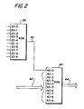
- a second memory in the form of ROM 40 is provided.
- the output of ROM 20 to bus 35 is fed to one input 40-0 of ROM 40, the output of ROM 20 serving in this embodiment as an address.
- a second input bus 42 provides additional address information from alternate inputs, which may for example comprise additional adjoining or neighborhood pixels, to ROM 40.
- the output of ROM 40 which comprises the pixel value associated with the address information input from ROM 20 together with image information from additional sources, is output via bus 44 to the user.
- the processing system herein described reduces the number of component parts required, provides a more economical processing system, and allows ready programming of the system.
Landscapes
- Engineering & Computer Science (AREA)
- Theoretical Computer Science (AREA)
- Physics & Mathematics (AREA)
- General Physics & Mathematics (AREA)
- Multimedia (AREA)
- General Engineering & Computer Science (AREA)
- Signal Processing (AREA)
- Image Processing (AREA)
- Memory System (AREA)
- Image Input (AREA)
Applications Claiming Priority (2)
| Application Number | Priority Date | Filing Date | Title |
|---|---|---|---|
| US06/304,429 US4430748A (en) | 1981-09-21 | 1981-09-21 | Image thresholding system |
| US304429 | 1999-05-03 |
Publications (3)
| Publication Number | Publication Date |
|---|---|
| EP0075470A2 true EP0075470A2 (de) | 1983-03-30 |
| EP0075470A3 EP0075470A3 (en) | 1986-03-19 |
| EP0075470B1 EP0075470B1 (de) | 1989-05-17 |
Family
ID=23176476
Family Applications (1)
| Application Number | Title | Priority Date | Filing Date |
|---|---|---|---|
| EP82304932A Expired EP0075470B1 (de) | 1981-09-21 | 1982-09-20 | Elektronisches Bildverarbeitungssystem |
Country Status (5)
| Country | Link |
|---|---|
| US (1) | US4430748A (de) |
| EP (1) | EP0075470B1 (de) |
| JP (1) | JPS5854472A (de) |
| CA (1) | CA1181864A (de) |
| DE (1) | DE3279703D1 (de) |
Cited By (5)
| Publication number | Priority date | Publication date | Assignee | Title |
|---|---|---|---|---|
| EP0189325A3 (en) * | 1985-01-23 | 1988-09-14 | Victor Company Of Japan, Limited | Picture information processing system |
| EP0160363A3 (en) * | 1984-04-28 | 1988-09-14 | Kabushiki Kaisha Toshiba | Binarizing system of picture image signals |
| EP0234590A3 (en) * | 1986-02-28 | 1989-09-20 | Dainippon Screen Mfg. Co., Ltd. | Method of and apparatus for generating high-resolution binary image data with respect to linear edges |
| EP0253264A3 (en) * | 1986-07-08 | 1990-08-22 | Sumitomo Electric Industries Limited | Binary coding circuit for ocr |
| EP0267968A4 (en) * | 1986-05-27 | 1990-12-27 | Fanuc Ltd | Image processor |
Families Citing this family (22)
| Publication number | Priority date | Publication date | Assignee | Title |
|---|---|---|---|---|
| US5666444A (en) * | 1982-04-06 | 1997-09-09 | Canon Kabushiki Kaisha | Image processing apparatus |
| GB2120896B (en) * | 1982-04-06 | 1987-01-28 | Canon Kk | Half-tone facsimile system |
| JPS59223062A (ja) * | 1983-06-01 | 1984-12-14 | Canon Inc | 画像読取装置 |
| IL71878A (en) * | 1984-05-21 | 1987-11-30 | Elscint Ltd | Intensity level windowing system for image displays |
| JPS60254279A (ja) * | 1984-05-31 | 1985-12-14 | Fuji Electric Co Ltd | 2値化しきい値の決定方法 |
| JPS6187471A (ja) * | 1984-09-17 | 1986-05-02 | Canon Inc | 画像処理システム |
| US4729098A (en) * | 1985-06-05 | 1988-03-01 | General Electric Company | System and method employing nonlinear interpolation for the display of surface structures contained within the interior region of a solid body |
| US4914623A (en) * | 1986-09-18 | 1990-04-03 | Hudson-Allen Limited | Digital processing of sensor signals for reading binary storage media |
| US4816914A (en) * | 1987-01-07 | 1989-03-28 | Pictel Corporation | Method and apparatus for efficiently encoding and decoding image sequences |
| US4849810A (en) * | 1987-06-02 | 1989-07-18 | Picturetel Corporation | Hierarchial encoding method and apparatus for efficiently communicating image sequences |
| US4982294A (en) * | 1987-07-24 | 1991-01-01 | Eastman Kodak Company | Apparatus for enhancing and thresholding scanned microfilm images and methods for use therein |
| US4853795A (en) * | 1987-07-24 | 1989-08-01 | Eastman Kodak Company | Forward look ahead techniques for tracking background and noise levels in scanned video images |
| US4868670A (en) * | 1987-07-24 | 1989-09-19 | Eastman Kodak Company | Apparatus and method for improving the compressibility of an enhanced image through use of a momentarily varying threshold level |
| US5042076A (en) * | 1988-12-02 | 1991-08-20 | Electrocom Automation, Inc. | Programmable optical character recognition |
| US4991223A (en) * | 1988-06-30 | 1991-02-05 | American Innovision, Inc. | Apparatus and method for recognizing image features using color elements |
| US5097520A (en) * | 1989-01-20 | 1992-03-17 | Ricoh Company, Ltd. | Method of obtaining optimum threshold values |
| US5087965A (en) * | 1989-06-28 | 1992-02-11 | American Innovision, Inc. | Recognition of image colors using arbitrary shapes in color space |
| US5041920A (en) * | 1989-11-15 | 1991-08-20 | Xerox Corporation | Image halftone generation by static RAM look-up table |
| US5489918A (en) * | 1991-06-14 | 1996-02-06 | Rockwell International Corporation | Method and apparatus for dynamically and adjustably generating active matrix liquid crystal display gray level voltages |
| AU2510792A (en) * | 1991-08-23 | 1993-03-16 | United Parcel Service Of America, Inc. | Method and apparatus for compensation for non-uniform illumination |
| US5602653A (en) * | 1994-11-08 | 1997-02-11 | Xerox Corporation | Pixel pair grid halftoning for a hyperacuity printer |
| US6121961A (en) * | 1996-08-06 | 2000-09-19 | Feldman; Bernard | String addressing of passive matrix displays |
Family Cites Families (16)
| Publication number | Priority date | Publication date | Assignee | Title |
|---|---|---|---|---|
| US3573789A (en) | 1968-12-13 | 1971-04-06 | Ibm | Method and apparatus for increasing image resolution |
| US3800078A (en) | 1972-12-18 | 1974-03-26 | Ibm | Digitally compensated scanning system |
| FR2258064A1 (en) * | 1973-10-05 | 1975-08-08 | Takachiho Koeki Kk | Graphic display system using point diagrams - uses series of bistable memory elements, detectors and computer |
| US3961132A (en) | 1974-07-15 | 1976-06-01 | Log Etronics Inc. | Sequential image-modulated dot-area recording |
| DE2458119C3 (de) | 1974-12-09 | 1980-08-14 | Siemens Ag, 1000 Berlin Und 8000 Muenchen | Verfahren und Anordnung zur Faksimilecodierung |
| JPS52107723A (en) | 1974-12-28 | 1977-09-09 | Seikosha Kk | Device for forming picture |
| US4003024A (en) | 1975-10-14 | 1977-01-11 | Rockwell International Corporation | Two-dimensional binary data enhancement system |
| US4084195A (en) | 1976-12-30 | 1978-04-11 | International Business Machines Corporation | Image data remapping system |
| US4149145A (en) | 1977-02-17 | 1979-04-10 | Xerox Corporation | Fax processor |
| US4129853A (en) | 1977-09-26 | 1978-12-12 | International Business Machines Corporation | Method and apparatus for producing compensated signals for individual light sensors arranged in a predetermined relation |
| US4215414A (en) | 1978-03-07 | 1980-07-29 | Hughes Aircraft Company | Pseudogaussian video output processing for digital display |
| US4242678A (en) | 1978-07-17 | 1980-12-30 | Dennison Manufacturing Company | Variable size character generation using neighborhood-derived shapes |
| JPS5537092A (en) | 1978-09-05 | 1980-03-14 | Ibm | Mode switch for setting threshold value |
| US4225861A (en) | 1978-12-18 | 1980-09-30 | International Business Machines Corporation | Method and means for texture display in raster scanned color graphic |
| US4290049A (en) * | 1979-09-10 | 1981-09-15 | Environmental Research Institute Of Michigan | Dynamic data correction generator for an image analyzer system |
| US4352105A (en) | 1979-09-25 | 1982-09-28 | Radiation Dynamics, Inc. | Display system |
-
1981
- 1981-09-21 US US06/304,429 patent/US4430748A/en not_active Expired - Lifetime
-
1982
- 1982-07-27 CA CA000408157A patent/CA1181864A/en not_active Expired
- 1982-09-10 JP JP57157964A patent/JPS5854472A/ja active Pending
- 1982-09-20 DE DE8282304932T patent/DE3279703D1/de not_active Expired
- 1982-09-20 EP EP82304932A patent/EP0075470B1/de not_active Expired
Cited By (5)
| Publication number | Priority date | Publication date | Assignee | Title |
|---|---|---|---|---|
| EP0160363A3 (en) * | 1984-04-28 | 1988-09-14 | Kabushiki Kaisha Toshiba | Binarizing system of picture image signals |
| EP0189325A3 (en) * | 1985-01-23 | 1988-09-14 | Victor Company Of Japan, Limited | Picture information processing system |
| EP0234590A3 (en) * | 1986-02-28 | 1989-09-20 | Dainippon Screen Mfg. Co., Ltd. | Method of and apparatus for generating high-resolution binary image data with respect to linear edges |
| EP0267968A4 (en) * | 1986-05-27 | 1990-12-27 | Fanuc Ltd | Image processor |
| EP0253264A3 (en) * | 1986-07-08 | 1990-08-22 | Sumitomo Electric Industries Limited | Binary coding circuit for ocr |
Also Published As
| Publication number | Publication date |
|---|---|
| EP0075470B1 (de) | 1989-05-17 |
| DE3279703D1 (en) | 1989-06-22 |
| JPS5854472A (ja) | 1983-03-31 |
| CA1181864A (en) | 1985-01-29 |
| US4430748A (en) | 1984-02-07 |
| EP0075470A3 (en) | 1986-03-19 |
Similar Documents
| Publication | Publication Date | Title |
|---|---|---|
| EP0075470A2 (de) | Elektronisches Bildverarbeitungssystem | |
| US5034990A (en) | Edge enhancement error diffusion thresholding for document images | |
| US5838463A (en) | Binary image processor | |
| KR960014303B1 (ko) | 화상 처리 장치 | |
| CA2077278A1 (en) | Halftoning with enhanced dynamic range and edge enhanced error diffusion | |
| US6331902B1 (en) | System and method for digital color image processing | |
| US4891714A (en) | Apparatus for non-linear error diffusion thresholding of multilevel video images | |
| EP0451579B1 (de) | Bildlesevorrichtung und Verfahren zur Verbesserung von Formumrissen | |
| US5784100A (en) | Apparatus and method for performing shading correction by multiplying a differential shading correction factor and input image data | |
| US5696601A (en) | System and method for redistributing error values from an error diffusion process | |
| US5499111A (en) | Image signal processing apparatus | |
| US4668989A (en) | Fading circuit for video signals | |
| EP0182243A2 (de) | Bildsignalfilterung | |
| JPS58220563A (ja) | 文字図形画像抽出方式 | |
| GB2223643A (en) | Data processing apparatus | |
| EP0189943B1 (de) | Parallel- Bildverarbeitungsgerät | |
| US4817173A (en) | Image contour detecting apparatus | |
| EP0145181A2 (de) | Halogenerator für die Anzeige von Symbolen auf Kathodenstrahlröhren | |
| US5038387A (en) | Method of enhancing border of region included in image | |
| JPH0799543B2 (ja) | 画像処理装置 | |
| EP0542267B1 (de) | Korrekturschaltung für Bildabtaster | |
| JP2601156B2 (ja) | 画像処理装置 | |
| JP2934971B2 (ja) | 画像2値化処理装置 | |
| JPH0668250A (ja) | 画像処理装置 | |
| JPH0818783A (ja) | 画像処理装置 |
Legal Events
| Date | Code | Title | Description |
|---|---|---|---|
| PUAI | Public reference made under article 153(3) epc to a published international application that has entered the european phase |
Free format text: ORIGINAL CODE: 0009012 |
|
| AK | Designated contracting states |
Designated state(s): DE FR GB IT |
|
| PUAL | Search report despatched |
Free format text: ORIGINAL CODE: 0009013 |
|
| AK | Designated contracting states |
Kind code of ref document: A3 Designated state(s): DE FR GB IT |
|
| 17P | Request for examination filed |
Effective date: 19860915 |
|
| 17Q | First examination report despatched |
Effective date: 19870602 |
|
| GRAA | (expected) grant |
Free format text: ORIGINAL CODE: 0009210 |
|
| AK | Designated contracting states |
Kind code of ref document: B1 Designated state(s): DE FR GB IT |
|
| REF | Corresponds to: |
Ref document number: 3279703 Country of ref document: DE Date of ref document: 19890622 |
|
| ET | Fr: translation filed | ||
| ITF | It: translation for a ep patent filed | ||
| PLBE | No opposition filed within time limit |
Free format text: ORIGINAL CODE: 0009261 |
|
| STAA | Information on the status of an ep patent application or granted ep patent |
Free format text: STATUS: NO OPPOSITION FILED WITHIN TIME LIMIT |
|
| 26N | No opposition filed | ||
| ITTA | It: last paid annual fee | ||
| PGFP | Annual fee paid to national office [announced via postgrant information from national office to epo] |
Ref country code: FR Payment date: 19990909 Year of fee payment: 18 |
|
| PGFP | Annual fee paid to national office [announced via postgrant information from national office to epo] |
Ref country code: GB Payment date: 19990915 Year of fee payment: 18 |
|
| PGFP | Annual fee paid to national office [announced via postgrant information from national office to epo] |
Ref country code: DE Payment date: 19990927 Year of fee payment: 18 |
|
| PG25 | Lapsed in a contracting state [announced via postgrant information from national office to epo] |
Ref country code: GB Free format text: LAPSE BECAUSE OF NON-PAYMENT OF DUE FEES Effective date: 20000920 |
|
| GBPC | Gb: european patent ceased through non-payment of renewal fee |
Effective date: 20000920 |
|
| PG25 | Lapsed in a contracting state [announced via postgrant information from national office to epo] |
Ref country code: FR Free format text: LAPSE BECAUSE OF NON-PAYMENT OF DUE FEES Effective date: 20010531 |
|
| PG25 | Lapsed in a contracting state [announced via postgrant information from national office to epo] |
Ref country code: DE Free format text: LAPSE BECAUSE OF NON-PAYMENT OF DUE FEES Effective date: 20010601 |
|
| REG | Reference to a national code |
Ref country code: FR Ref legal event code: ST |