EP0075491A2 - Apparat und Verfahren zum Anordnen von Halbleiterwürfeln - Google Patents
Apparat und Verfahren zum Anordnen von Halbleiterwürfeln Download PDFInfo
- Publication number
- EP0075491A2 EP0075491A2 EP82305005A EP82305005A EP0075491A2 EP 0075491 A2 EP0075491 A2 EP 0075491A2 EP 82305005 A EP82305005 A EP 82305005A EP 82305005 A EP82305005 A EP 82305005A EP 0075491 A2 EP0075491 A2 EP 0075491A2
- Authority
- EP
- European Patent Office
- Prior art keywords
- pellet
- plane
- supporting means
- adhesive tape
- apical
- Prior art date
- Legal status (The legal status is an assumption and is not a legal conclusion. Google has not performed a legal analysis and makes no representation as to the accuracy of the status listed.)
- Granted
Links
Images



Classifications
-
- H—ELECTRICITY
- H10—SEMICONDUCTOR DEVICES; ELECTRIC SOLID-STATE DEVICES NOT OTHERWISE PROVIDED FOR
- H10P—GENERIC PROCESSES OR APPARATUS FOR THE MANUFACTURE OR TREATMENT OF DEVICES COVERED BY CLASS H10
- H10P72/00—Handling or holding of wafers, substrates or devices during manufacture or treatment thereof
- H10P72/50—Handling or holding of wafers, substrates or devices during manufacture or treatment thereof for positioning, orientation or alignment
-
- H—ELECTRICITY
- H10—SEMICONDUCTOR DEVICES; ELECTRIC SOLID-STATE DEVICES NOT OTHERWISE PROVIDED FOR
- H10P—GENERIC PROCESSES OR APPARATUS FOR THE MANUFACTURE OR TREATMENT OF DEVICES COVERED BY CLASS H10
- H10P72/00—Handling or holding of wafers, substrates or devices during manufacture or treatment thereof
- H10P72/30—Handling or holding of wafers, substrates or devices during manufacture or treatment thereof for conveying, e.g. between different workstations
- H10P72/32—Handling or holding of wafers, substrates or devices during manufacture or treatment thereof for conveying, e.g. between different workstations between different workstations
- H10P72/3212—Handling or holding of wafers, substrates or devices during manufacture or treatment thereof for conveying, e.g. between different workstations between different workstations the substrates to be conveyed not being semiconductor wafers or large planar substrates, e.g. chips or lead frames
-
- H—ELECTRICITY
- H10—SEMICONDUCTOR DEVICES; ELECTRIC SOLID-STATE DEVICES NOT OTHERWISE PROVIDED FOR
- H10P—GENERIC PROCESSES OR APPARATUS FOR THE MANUFACTURE OR TREATMENT OF DEVICES COVERED BY CLASS H10
- H10P72/00—Handling or holding of wafers, substrates or devices during manufacture or treatment thereof
- H10P72/04—Apparatus for manufacture or treatment
- H10P72/0442—Apparatus for placing on an insulating substrate, e.g. tape
-
- Y—GENERAL TAGGING OF NEW TECHNOLOGICAL DEVELOPMENTS; GENERAL TAGGING OF CROSS-SECTIONAL TECHNOLOGIES SPANNING OVER SEVERAL SECTIONS OF THE IPC; TECHNICAL SUBJECTS COVERED BY FORMER USPC CROSS-REFERENCE ART COLLECTIONS [XRACs] AND DIGESTS
- Y10—TECHNICAL SUBJECTS COVERED BY FORMER USPC
- Y10S—TECHNICAL SUBJECTS COVERED BY FORMER USPC CROSS-REFERENCE ART COLLECTIONS [XRACs] AND DIGESTS
- Y10S269/00—Work holders
- Y10S269/903—Work holder for electrical circuit assemblages or wiring systems
-
- Y—GENERAL TAGGING OF NEW TECHNOLOGICAL DEVELOPMENTS; GENERAL TAGGING OF CROSS-SECTIONAL TECHNOLOGIES SPANNING OVER SEVERAL SECTIONS OF THE IPC; TECHNICAL SUBJECTS COVERED BY FORMER USPC CROSS-REFERENCE ART COLLECTIONS [XRACs] AND DIGESTS
- Y10—TECHNICAL SUBJECTS COVERED BY FORMER USPC
- Y10T—TECHNICAL SUBJECTS COVERED BY FORMER US CLASSIFICATION
- Y10T156/00—Adhesive bonding and miscellaneous chemical manufacture
- Y10T156/17—Surface bonding means and/or assemblymeans with work feeding or handling means
- Y10T156/1702—For plural parts or plural areas of single part
- Y10T156/1705—Lamina transferred to base from adhered flexible web or sheet type carrier
- Y10T156/1707—Discrete spaced laminae on adhered carrier
- Y10T156/171—Means serially presenting discrete base articles or separate portions of a single article
-
- Y—GENERAL TAGGING OF NEW TECHNOLOGICAL DEVELOPMENTS; GENERAL TAGGING OF CROSS-SECTIONAL TECHNOLOGIES SPANNING OVER SEVERAL SECTIONS OF THE IPC; TECHNICAL SUBJECTS COVERED BY FORMER USPC CROSS-REFERENCE ART COLLECTIONS [XRACs] AND DIGESTS
- Y10—TECHNICAL SUBJECTS COVERED BY FORMER USPC
- Y10T—TECHNICAL SUBJECTS COVERED BY FORMER US CLASSIFICATION
- Y10T156/00—Adhesive bonding and miscellaneous chemical manufacture
- Y10T156/17—Surface bonding means and/or assemblymeans with work feeding or handling means
- Y10T156/1702—For plural parts or plural areas of single part
- Y10T156/1712—Indefinite or running length work
- Y10T156/1734—Means bringing articles into association with web
-
- Y—GENERAL TAGGING OF NEW TECHNOLOGICAL DEVELOPMENTS; GENERAL TAGGING OF CROSS-SECTIONAL TECHNOLOGIES SPANNING OVER SEVERAL SECTIONS OF THE IPC; TECHNICAL SUBJECTS COVERED BY FORMER USPC CROSS-REFERENCE ART COLLECTIONS [XRACs] AND DIGESTS
- Y10—TECHNICAL SUBJECTS COVERED BY FORMER USPC
- Y10T—TECHNICAL SUBJECTS COVERED BY FORMER US CLASSIFICATION
- Y10T29/00—Metal working
- Y10T29/49—Method of mechanical manufacture
- Y10T29/49826—Assembling or joining
- Y10T29/49828—Progressively advancing of work assembly station or assembled portion of work
- Y10T29/49829—Advancing work to successive stations [i.e., assembly line]
-
- Y—GENERAL TAGGING OF NEW TECHNOLOGICAL DEVELOPMENTS; GENERAL TAGGING OF CROSS-SECTIONAL TECHNOLOGIES SPANNING OVER SEVERAL SECTIONS OF THE IPC; TECHNICAL SUBJECTS COVERED BY FORMER USPC CROSS-REFERENCE ART COLLECTIONS [XRACs] AND DIGESTS
- Y10—TECHNICAL SUBJECTS COVERED BY FORMER USPC
- Y10T—TECHNICAL SUBJECTS COVERED BY FORMER US CLASSIFICATION
- Y10T29/00—Metal working
- Y10T29/49—Method of mechanical manufacture
- Y10T29/49998—Work holding
Definitions
- This invention relates to an apparatus and method for arranging semiconductor pellets and more particularly to an apparatus and method for arranging groups of previously divided pellets in the matrix form at a prescribed distance.
- the known method of arranging semiconductor pellets in the above-mentioned manner uses a tape which is thermally expandable and on one side of which an adhesive layer is deposited. A semiconductor wafer is placed on the adhesive layer. The semiconductor wafer on the tape is cut up into a plurality of pellets by a dicing machine. The adhesive tape is thermally expanded to thereby separate the pellets from each other at a prescribed distance.
- the conventional method of arranging semiconductor pellets is accompanied with the drawbacks that the adhesive tape is not uniformly extended in all directions, presenting difficulties in effecting the precise arrangement of semiconductor pellets. Consequently when the semiconductor pellets separated on the adhesive tape are fixed tc the surface of a stem or wiring substrate just as separated, then the displacement of the pellets from the prescribed position often arises.
- the method of this invention is characterized by the step of transposing a matrix of closely contacting semiconductor pellets mounted from a first adhesive tape to a second adhesive tape in such a manner that the rows of pellets are separated from each other at a prescribed distance.
- the subject apparatus comprises a first pellet-supporting unit including an inclined plane and an apical plane contiguous thereto.
- the first adhesive tape on which the matrix of pellets is placed progressively travels by a first driving device along the inclined plane toward the apical plane so as to cause the rows of matrix of pellets to be set on the apical plane one after another.
- a second driving device which carries the second adhesive tape in a direction intersecting the columns of pellets at right angles with the adhesive plane of the second adhesive tape caused to face the first adhesive tape.
- a semiconductor pellet-arranging device further comprises a second pellet-supporting unit like the first one which is positioned below the second adhesive tape and spaced from the first one in the traveling direction of the first tape.
- a third adhesive tape whose adhesive plane is made to face the second adhesive tape is progressively carried by a fourth drive device for a prescribed distance along the inclined plane of the second pellet-supporting unit toward the apical plane thereof.
- a plurality of divided semiconductor pellets can be precisely separated at a prescribed distance, thereby offering a great advantage in effecting the simultaneous deposition of a plurality of semiconductor pellets on a stem or wiring substrate.
- Fig. 1 is a front view of a semiconductor pellet-arranging apparatus embodying this invention.
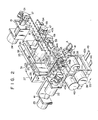
- Fig. 2 is a schematic fractional oblique view of this apparatus.
- the semiconductor pellet-arranging apparatus comprises a pair of sprocket wheels 16, 17 spaced from each other at a prescribed distance.
- Each sprocket wheel comprises a smaller diameter cylindrical body and a pair of larger diameter disks arranged on both sides of the smaller diameter cylindrical body.
- a plurality of sprockets are spatially formed on the outer periphery of each larger diameter disk.
- the sprocket wheels 16, 17 are respectively supported by support members 14, 15 fitted to frames 12, 13 in a state spatially positioned from a support stage 11 in parallel therewith.
- an adhesive tape B Stretched between the sprocket wheels 16, 17 is an adhesive tape B which is prepared from, for example, a polyimide film and coated with an adhesive agent, for example, silicone-based adhesive.
- the adhesive plane of the tape B is kept underside. Both edge portions of the adhesive tape B are respectively provided with linearly arranged sprocket holes SH corresponding to the projections (sprockets) of the sprocket wheels 16, 17.
- the adhesive tape B is pressed against the sprocket wheels 16, 17 by means of auxiliary rolls 20, 21 supported by proper levers 18, 19 fitted to the support members 14, 15.
- the auxiliary rolls 20, 21 are each comprised of a smaller diameter cylindrical body and a pair of larger diameter disks fitted to both ends of said cylindrical body.
- Formed in the outer peripheral wall of each larger diameter disk is an annular groove having a slightly larger width than each projection of the sprocket wheels 16, 17 and a depth slightly shallower than the height of said each projection. Both edges of the adhesive tape B on which a plurality of sprocket holes SH are linearly arranged are held between the larger diameter disks of the sprocket wheels 16, 17 and larger diameter disks of the auxiliary rolls 20, 21.
- the sprocket wheel 16 is connected to a stepping motor 23 through a harmonic drive system 22.
- the sprocket wheel 17 is connected to a torque motor 24.
- the harmonic drive system 22 smoothly transmits the drive force of the stepping motor 23 to the sprocket wheel 16.
- the interlocking operation of the stepping motor 23 and torque motor 24 causes the adhesive tape B to progressively travel in a direction indicated by an arrow BD for a prescribed distance in a stretched state.
- Two parallel guide rods 25, 26 extend between the frames 12, 13 in parallel with the adhesive tape B.
- a slide board 30 is slidably fitted to the support block 27 by means of guide rails 28, 29.
- a press board 31 is integrally formed with the slide board 30 so as to horizontally project from the lower end of the slide board 30 over the adhesive tape B.
- a transparent board 32 is fitted into the central part of the press board 31. The press board 31 vertically moves over the slide board along the rails 28, 29 by the manual operation of a rod 33 fitted to said slide board 30.
- a semiconductor pellet-supporting unit 34 is positioned below that portion of the adhesive tape B which is stretched between the frames 12, 13 at a prescribed distance from the adhesive tape B (said distance is chosen to be longer than the height of the later described semiconductor pellet).
- This semiconductor pellet-supporting unit 34 consists of a block 34A having a substantially triangular cross section (hereinafter referred to as "a triangular block").
- the apical plane of the triangular block 34A is rendered parallel with the traveling direction BD of the adhesive tape B.
- the triangular block 34A is supported on a support member 35 by means of rod members 34B, 34B integrally formed with the triangular block 34A.
- a pair of sprocket wheels 36, 37 having the same construction as the sprocket wheels 16, 17 are symmetrically positioned with respect to the pellet-supporting unit 34.
- An adhesive tape A both lateral edge portions of which are provided with linearly arranged sprocket holes like the adhesive tape B is stretched over the pellet-supporting unit 34 along the inclined planes 34C and 35D thereof between the sprocket wheels 36, 37 with the adhesive plane of the tape A kept upward.
- a semiconductor pellet matrix (not shown in Figs. 1 and 2) is mounted on the adhesive plane of the tape A.
- the sprocket wheel 36 is connected to a stepping motor 39 through a harmonic drive system 38.
- the other sprocket wheel 37 is connected to a torque motor 40.
- the interlocking operation of the stepping motor 39 and torque motor 40 causes the adhesive tape A to ride over the inclined plane 34C of the triangular pellet-supporting unit 34 and to come down the inclined plane 34D in a stretched state between the sprocket wheels 36, 37, at a prescribed speed.
- the adhesive tape A is pressed against the sprocket wheels 36, 37 by the auxiliary rolls 41, 42 having the same construction as the auxiliary rolls 21, 22.
- the harmonic drive system 38 and stepping motor 39 are supported by a frame 43A, and the torque motor 40 is supported by a frame 43B.
- the support frames 43A, 43B and support member 35 which are mounted on a stage 46 are made to reciprocate for a prescribed distance by a proper drive unit (not shown) along guide rails 44, 45 laid on the support stage 11 in a direction intersecting the traveling direction BD of the adhesive tape B at right angles.
- a second triangular pellet-supporting unit 47 having the similar construction to the pellet-supporting unit 34 is provided at a spot spaced from the pellet-supporting unit 34 as viewed from the traveling direction BD of the adhesive tape B.
- the apical plane of the second triangular pellet-supporting unit 47 extends in a direction intersecting the traveling direction BD of the adhesive tape B at right angles.
- Sprocket wheels 48, 49 having the same construction as the sprocket wheels 36, 37 are provided on both sides of the second triangular pellet-supporting unit 47.
- the sprocket wheel 48 is connected to a stepping motor 51 through a harmonic drive system 50.
- An adhesive tape C provided with sprocket holes having the same shape as those drilled in the adhesive tape B is stretched over the second triangular pellet-supporting unit 47 between the sprocket wheels 48, 49 with the adhesive plane of the tape C kept upward.
- the interlocking operation of the stepping motor 51 and torque motor 52 causes the adhesive tape C to ride over the inclined plane 47A of the second triangular pellet-supporting unit 47 in a stretched state between the sprocket wheels 48, 49 and come down the inclined plane 47B of the second triangular pellet-supporting unit 47 at a prescribed speed.
- the adhesive tape C is pressed against the sprocket wheels 48, 49 by means of auxiliary rolls 53, 54 having the same construction as the auxiliary rolls 41, 42.
- the stepping motor 51 and harmonic drive system 50 are supported by a frame 55.
- the torque motor 52 is supported by a frame 56.
- a plurality of pellet matrices each comprising a plurality of rows of pellets and a plurality of columns of pellets are spatially mounted on the adhesive plane of the tape A.
- the pellets of the columns and rows contact each other.
- an adhesive layer having a particular shape (for example, a rectangular shape) is mounted on a plurality of spots spaced from each other at a prescribed distance.
- a semiconductor wafer for example, GaP wafer, in which prescribed semiconductor regions are formed is attached to each adhesive layer.
- the wafer is divided into a plurality of square pellets, each side of which measures, for example, 0.3 mm, by means of a dicing machine.
- the peripheral section of the wafer which is not attached to the adhesive layer is removed.
- a semiconductor wafer divided into a plurality of matrix-arranged pellets on a separate adhesive tape, and mount the tape A on the wafer with its adhesive plane made to contact the surface of the wafer, and apply pressure on the superposed mass by a rectangular press board, thereby transposing a square pellet matrix to the adhesive plane of the tape A.
- the tape A on which a plurality of pellet matrices are mounted is stretched over the triangular pellet-supporting unit 34 between the sprocket wheels 36, 37, with the adhesive plane, that is, the pellet matrices- bearing plane of the tape A kept upward (see Fig. 3).
- a tape B is stretched between the spatially arranged sprocket wheels 16, 17 with the adhesive plane of the tape B kept downward.
- the tape B is preferred to consist of a transparent material.
- the tape C is stretched over the triangular pellet-supporting unit 47 between the sprocket wheels 48, 49 with the adhesive plane of the tape C kept upward.
- the support stage 46 travels along the guide rails 44, 45 to be brought below the left side of the tape B as viewed from its traveling direction BD. Later, when the stepping motor 39 and torque motor 40 are driven, the tape A is carried over the triangular pellet-supporting unit 34 in a stretched state in a direction indicated by the arrow AD1. When the first row 101 of the pellet matrix 100 mounted on the tape A is brought to the apical plane of the triangular pellet-supporting unit 34 as seen from Fig. 3, the tape A is brought to rest.
- the support stage 46 When one pellet row is transposed to the tape B, the support stage 46 is shifted in the direction of an arrow SD to cause the triangular pellet-supporting unit 34 to stop at a spot separated from its first position for a prescribed distance. Again the stepping motor 39 and torque motor 40 are driven to shift the tape A, causing the second pellet row 102 on the tape A to be set on the apical plane of the triangular pellet-supporting unit 34. At this time, the tape B is pressed against the second pellet row 102 to transpose the second pellet row to the tape B.
- Repetition of the above-mentioned operation causes the pellet rows 101, 102, 103, ... on the tape A to be arranged across the tape B at a prescribed distance.
- the tape B is moved by the stepping motor 23 and torque motor 24 for a prescribed distance in traveling direction BD and is brought to rest there.
- the above-mentioned operation is carried out in succession to cause the respective pellet rows of the tape A to be spatially arranged across the tape B.
- the tape B on the adhesive plane of which a plurality of pellet rows are spatially arranged in the crosswise direction is progressively forwarded.
- the support block 27 is made to slide along the guide rods 25, 26.
- the press board 31 is brought downward while being kept above the triangular pellet-supporting unit 47.
- the first pellet column transposed to the tape B is pressed against the tape C on the apical plane of the triangular pellet-supporting unit 47.
- the press board 31 is lifted, the tape B regains its original stretched condition.
- the pellet column set on the tape B is transposed to the tape C on the apical plane of the triangular pellet-supporting unit 47.
- the tape C is shifted in the direction of an arrow CD for a prescribed distance by the interlocking operation of the stepping motor 51 and torque motor 52.
- the tape B is also made to travel, until the second pellet column is positioned above the apical plane of the triangular pellet-supporting unit 47.
- the press board 31 is brought down to cause the second pellet column to be pressed against the tape C on the apical plane of the triangular pellet-supporting unit 47.
- the second pellet column is transcribed to the tape C by lifting the press board.
- a microscope 57 (Fig. 1) may be mounted on the support block 27 so as to be positioned above the transparent plate 32 fitted to the center of the press board 31. It is possible to press the tape B against the tape A and/or tape C while confirming by the microscope 57 that the pellet row set on the tape A is positioned on the apical plane of the triangular pellet-supporting unit 34 and/or the pellet column mounted on the tape B lies on the apical plane of the triangular pellet-supporting unit 47.
- a pellet row be positioned on the apical plane of the first triangular pellet-supporting unit 34 under a substantially stable condition, and also the unit 34 be possessed of such an apical plane as allows for the easy transposition of said pellet row to the tape B.
- the cross section of the apical plane of the triangular pellet-supporting unit 34 of Fig. 5 has a convex curved outline 34E having a relatively large curvature radius.
- the apical plane of the triangular pellet-supporting unit 34 of Fig. 6 has a flat cross section 34E'.
- the width W of the cross section 34E' is preferred to be smaller than the length L of each side of a square pellet P, because the pellet row has to be easily transposed to the tape B.
- an angle defined by the inclined plane 34C with the incline plane 34D is chosen to be the same as in Fig. 5.
- the apical plane of the second triangular pellet-supporting unit 47 is preferred to have a flat cross section having substantially the same length as one side of a square pellet. In this case, too, two inclined planes of said second triangular pellet-supporting unit 47 are chosen to define an angle having the same magnitude as in the aforementioned case. Obviously, the apical planes of the first and second triangular pellet-supporting units 34, 47 have a length equal to or larger than the row and column of the pellet matrix, respectively.
- the tape A was made to travel only in the direction AD1.
- the tape A it is possible to allow the tape A to run also in the opposite direction AD2 (Fig. 3), set two semiconductor pellets emitting different, for example, red and green lights close to each other, and arrange picture elements emitting a light having a mixed color (yellow) on the tape C in a state spaced from each other at a prescribed distance.
- a matrix of red light-emitting diode pellets and a matrix of green light-emitting diode pellets are mounted on the tape A in advance.
- the tape A is stretched between the sprocket wheels 36, 37, causing the above-mentioned matrices to be respectively positioned on both sides of the triangular pellet-supporting unit 34.
- the support stage 46 is retracted to slightly shift the triangular pellet-supporting unit 34.
- the step motor 39 is driven in the reverse direction to cause the tape A to travel in the direction AD2, thereby setting one row of the other matrix of green light-emitting pellets on the apical plane of the triangular pellet-supporting unit 34.
- the row of green light-emitting pellets is transposed in the proximity of the row of red light-emitting pellets on the tape B.
- a second row of red light-emitting pellets are transposed to the tape B in a state spaced from the first row of green light-emitting pellets at a prescribed distance.
- a second row of green light-emitting pellets is transposed to the tape B in the proximity of the second row of red light-emitting pellets. Thereafter the same operation is repeated.
- the tape B may be formed of an endless tape.
- the sliding of the support block 27 and the vertical movement of the press board 31 can be electrically controlled by proper drive means. It is also possible to automatically control the operation of the whole semiconductor pellet-arranging apparatus by means of a computer.
- the tape B may be removed from the sprocket wheels 16 and 17, and the tape A from the sprocket wheels 36 and 37. Then, the tape B now bearing the semiconductor pellets is set over the pellet-supporting unit 34 between the sprocket wheels 36 and 37 with the adhesive plane thereof kept upward.
- a new adhesive tape is set between the sprocket wheels 16 and 17 with its adhesive plane thereof kept downward. Thereafter, the similar operations to those described above with respect to the tape A and the tape B is applied to the tape B bearing the pellets and the new tape. As a result, a pellet matrix as shown in Fig. 4 is formed on the new tape.
Landscapes
- Container, Conveyance, Adherence, Positioning, Of Wafer (AREA)
- Dicing (AREA)
- Die Bonding (AREA)
Applications Claiming Priority (2)
| Application Number | Priority Date | Filing Date | Title |
|---|---|---|---|
| JP148844/81 | 1981-09-22 | ||
| JP56148844A JPS5851530A (ja) | 1981-09-22 | 1981-09-22 | 半導体ペレツト配列装置および方法 |
Publications (3)
| Publication Number | Publication Date |
|---|---|
| EP0075491A2 true EP0075491A2 (de) | 1983-03-30 |
| EP0075491A3 EP0075491A3 (en) | 1983-10-12 |
| EP0075491B1 EP0075491B1 (de) | 1987-01-14 |
Family
ID=15461997
Family Applications (1)
| Application Number | Title | Priority Date | Filing Date |
|---|---|---|---|
| EP82305005A Expired EP0075491B1 (de) | 1981-09-22 | 1982-09-22 | Apparat und Verfahren zum Anordnen von Halbleiterwürfeln |
Country Status (5)
| Country | Link |
|---|---|
| US (1) | US4465543A (de) |
| EP (1) | EP0075491B1 (de) |
| JP (1) | JPS5851530A (de) |
| KR (1) | KR860000711B1 (de) |
| DE (1) | DE3275150D1 (de) |
Cited By (5)
| Publication number | Priority date | Publication date | Assignee | Title |
|---|---|---|---|---|
| US4590667A (en) * | 1984-08-22 | 1986-05-27 | General Instrument Corporation | Method and apparatus for assembling semiconductor devices such as LEDs or optodetectors |
| FR2721295A1 (fr) * | 1994-03-22 | 1995-12-22 | Teikoku Seiki Kk | Dispositif d'extension de bande destinée à un appareil de production de semiconducteurs et à un appareil de production de semiconducteurs comportant ce dispositif d'extension de bande. |
| WO2003085702A1 (de) * | 2002-04-04 | 2003-10-16 | Georg Rudolf Sillner | Verfahren zum verarbeiten von elektrischen bauelementen, insbesondere von halbleiterchips, sowie vorrichtung zum durchführen des verfahrens |
| US7364983B2 (en) | 2005-05-04 | 2008-04-29 | Avery Dennison Corporation | Method and apparatus for creating RFID devices |
| US7560303B2 (en) | 2006-11-07 | 2009-07-14 | Avery Dennison Corporation | Method and apparatus for linear die transfer |
Families Citing this family (5)
| Publication number | Priority date | Publication date | Assignee | Title |
|---|---|---|---|---|
| US4862827A (en) * | 1988-06-28 | 1989-09-05 | Wacker-Chemie Gmbh | Apparatus for coating semiconductor components on a dielectric film |
| FR2794443B1 (fr) * | 1999-06-02 | 2001-06-22 | Commissariat Energie Atomique | Procede de transfert d'elements et dispositif permettant ledit transfert |
| FR2798513B1 (fr) * | 1999-09-10 | 2002-03-22 | Gemplus Card Int | Procede pour le report de microplaquettes de circuit integre et dispositif utilise |
| JP4491948B2 (ja) * | 2000-10-06 | 2010-06-30 | ソニー株式会社 | 素子実装方法および画像表示装置の製造方法 |
| DE102008051061B3 (de) * | 2008-10-09 | 2010-04-08 | Mr Etikettiertechnik Gmbh & Co. Kg | Etikettiervorrichtung |
Family Cites Families (16)
| Publication number | Priority date | Publication date | Assignee | Title |
|---|---|---|---|---|
| US3149765A (en) * | 1963-05-28 | 1964-09-22 | Western Electric Co | Apparatus for removing waffrs from semiconductor slices |
| US3743558A (en) * | 1969-10-02 | 1973-07-03 | Western Electric Co | Method of compliant bonding |
| GB1271128A (en) * | 1969-11-01 | 1972-04-19 | Teledyne Inc | Method and apparatus for sorting semi-conductor devices |
| US3708372A (en) * | 1970-08-25 | 1973-01-02 | Land Bros Inc | Apparatus for performing intermittent operations on a web |
| US3715258A (en) * | 1971-03-23 | 1973-02-06 | Bancroft H Corp | Integrated circuit die bonding apparatus |
| US3785903A (en) * | 1971-10-01 | 1974-01-15 | Western Electric Co | Loading of compliant tape |
| US3949925A (en) * | 1974-10-03 | 1976-04-13 | The Jade Corporation | Outer lead bonder |
| US3894633A (en) * | 1974-10-24 | 1975-07-15 | Western Electric Co | Method and apparatus for sorting articles |
| US4029536A (en) * | 1976-04-07 | 1977-06-14 | Western Electric Company, Inc. | Methods of and apparatus for mounting articles to a carrier member |
| US4021292A (en) * | 1976-05-14 | 1977-05-03 | Universal Instruments Corporation | Taped belt electronic component centering device |
| US4061521A (en) * | 1976-07-19 | 1977-12-06 | Color Communications, Inc. | Method and apparatus for manufacture of swatch bearing sheets |
| US4142662A (en) * | 1978-01-27 | 1979-03-06 | Bell Telephone Laboratories, Incorporated | Method of bonding microelectronic chips |
| NL7905518A (nl) * | 1978-07-19 | 1980-01-22 | Matsushita Electric Ind Co Ltd | Werkwijze voor het monteren van elektronische delen. |
| DE2845913A1 (de) * | 1978-10-21 | 1980-04-24 | Heller Geb Gmbh Maschf | Arbeitsstation fuer eine fertigungsstrasse, insbesondere fuer eine montagemaschine |
| US4291867A (en) * | 1979-06-25 | 1981-09-29 | Rockwell International Corporation | Automatic insertion universal work holding system |
| NL8201653A (nl) * | 1982-04-21 | 1983-11-16 | Philips Nv | Werkwijze en inrichting voor het plaatsen van chipvormige electrische en/of electronische onderdelen op een substraat. |
-
1981
- 1981-09-22 JP JP56148844A patent/JPS5851530A/ja active Pending
-
1982
- 1982-09-22 KR KR8204285A patent/KR860000711B1/ko not_active Expired
- 1982-09-22 EP EP82305005A patent/EP0075491B1/de not_active Expired
- 1982-09-22 US US06/421,099 patent/US4465543A/en not_active Expired - Lifetime
- 1982-09-22 DE DE8282305005T patent/DE3275150D1/de not_active Expired
Cited By (6)
| Publication number | Priority date | Publication date | Assignee | Title |
|---|---|---|---|---|
| US4590667A (en) * | 1984-08-22 | 1986-05-27 | General Instrument Corporation | Method and apparatus for assembling semiconductor devices such as LEDs or optodetectors |
| FR2721295A1 (fr) * | 1994-03-22 | 1995-12-22 | Teikoku Seiki Kk | Dispositif d'extension de bande destinée à un appareil de production de semiconducteurs et à un appareil de production de semiconducteurs comportant ce dispositif d'extension de bande. |
| WO2003085702A1 (de) * | 2002-04-04 | 2003-10-16 | Georg Rudolf Sillner | Verfahren zum verarbeiten von elektrischen bauelementen, insbesondere von halbleiterchips, sowie vorrichtung zum durchführen des verfahrens |
| US7364983B2 (en) | 2005-05-04 | 2008-04-29 | Avery Dennison Corporation | Method and apparatus for creating RFID devices |
| US7989313B2 (en) | 2005-05-04 | 2011-08-02 | Avery Dennison Corporation | Method and apparatus for creating RFID devices |
| US7560303B2 (en) | 2006-11-07 | 2009-07-14 | Avery Dennison Corporation | Method and apparatus for linear die transfer |
Also Published As
| Publication number | Publication date |
|---|---|
| EP0075491A3 (en) | 1983-10-12 |
| KR840001776A (ko) | 1984-05-16 |
| DE3275150D1 (en) | 1987-02-19 |
| US4465543A (en) | 1984-08-14 |
| EP0075491B1 (de) | 1987-01-14 |
| KR860000711B1 (ko) | 1986-06-07 |
| JPS5851530A (ja) | 1983-03-26 |
Similar Documents
| Publication | Publication Date | Title |
|---|---|---|
| US4465543A (en) | Apparatus and method for arranging semiconductor pellets | |
| DE69700347T2 (de) | Haftverfahren für CD-Platte | |
| RU2004115754A (ru) | Способы и системы для обработки подложки с использованием динамических жидких менисков | |
| IL125189A (en) | Precision cutting apparatus and cutting method using the same | |
| JPH0271580A (ja) | 回路基板分離装置とその方法 | |
| CN109423601B (zh) | 夹持装置及包括其的掩模组件制造装置 | |
| KR860002353A (ko) | 쉬이트 혹은 판 물질 위에 배치된 형판들의 위치를 인지하여 정하는 방법 | |
| US4138774A (en) | Panel positioning apparatus | |
| EP4360132A1 (de) | Verfahren und system zur herstellung mikrostrukturierter komponenten | |
| CN110112091A (zh) | 一种批量转移晶片裸片的装置 | |
| EP0289045B1 (de) | Vorrichtung zur Herstellung von Halbleiter-Bauelementen | |
| US4997792A (en) | Method for separation of diode array chips during fabrication thereof | |
| JP5460374B2 (ja) | 半導体装置の製造方法 | |
| CN110817406B (zh) | 一种自动转料机构的作业方法 | |
| KR20050003256A (ko) | 액정 패널 배치 구조 및 액정 패널 노광 방법 | |
| JPS5946429B2 (ja) | 発光表示装置の製造方法 | |
| JPH0212944A (ja) | 半導体装置製造用シート拡大装置 | |
| US4987686A (en) | Step and repeat apparatus | |
| EP0823193B1 (de) | Vorrichtung zur herstellung von mehrschichtschaltungen | |
| US3327400A (en) | Method and apparatus for relief paste-up process | |
| CN117055147B (zh) | 一种衍射光波导的裂片方法 | |
| US5042165A (en) | Step and repeat apparatus | |
| CN211055575U (zh) | 一种自动转料机构 | |
| CN211055576U (zh) | 一种快速转料机构 | |
| JP3011700B1 (ja) | 装飾材の製造装置 |
Legal Events
| Date | Code | Title | Description |
|---|---|---|---|
| PUAI | Public reference made under article 153(3) epc to a published international application that has entered the european phase |
Free format text: ORIGINAL CODE: 0009012 |
|
| 17P | Request for examination filed |
Effective date: 19821006 |
|
| AK | Designated contracting states |
Designated state(s): DE FR GB |
|
| PUAL | Search report despatched |
Free format text: ORIGINAL CODE: 0009013 |
|
| AK | Designated contracting states |
Designated state(s): DE FR GB |
|
| RAP1 | Party data changed (applicant data changed or rights of an application transferred) |
Owner name: KABUSHIKI KAISHA TOSHIBA |
|
| GRAA | (expected) grant |
Free format text: ORIGINAL CODE: 0009210 |
|
| AK | Designated contracting states |
Kind code of ref document: B1 Designated state(s): DE FR GB |
|
| REF | Corresponds to: |
Ref document number: 3275150 Country of ref document: DE Date of ref document: 19870219 |
|
| ET | Fr: translation filed | ||
| PLBE | No opposition filed within time limit |
Free format text: ORIGINAL CODE: 0009261 |
|
| STAA | Information on the status of an ep patent application or granted ep patent |
Free format text: STATUS: NO OPPOSITION FILED WITHIN TIME LIMIT |
|
| 26N | No opposition filed | ||
| PGFP | Annual fee paid to national office [announced via postgrant information from national office to epo] |
Ref country code: FR Payment date: 19940909 Year of fee payment: 13 |
|
| PGFP | Annual fee paid to national office [announced via postgrant information from national office to epo] |
Ref country code: GB Payment date: 19940913 Year of fee payment: 13 |
|
| PGFP | Annual fee paid to national office [announced via postgrant information from national office to epo] |
Ref country code: DE Payment date: 19940921 Year of fee payment: 13 |
|
| PG25 | Lapsed in a contracting state [announced via postgrant information from national office to epo] |
Ref country code: GB Effective date: 19950922 |
|
| GBPC | Gb: european patent ceased through non-payment of renewal fee |
Effective date: 19950922 |
|
| PG25 | Lapsed in a contracting state [announced via postgrant information from national office to epo] |
Ref country code: FR Effective date: 19960531 |
|
| PG25 | Lapsed in a contracting state [announced via postgrant information from national office to epo] |
Ref country code: DE Effective date: 19960601 |
|
| REG | Reference to a national code |
Ref country code: FR Ref legal event code: ST |